EP3926809A1 - Convertisseur de puissance resonant - Google Patents
Convertisseur de puissance resonant Download PDFInfo
- Publication number
- EP3926809A1 EP3926809A1 EP21177462.5A EP21177462A EP3926809A1 EP 3926809 A1 EP3926809 A1 EP 3926809A1 EP 21177462 A EP21177462 A EP 21177462A EP 3926809 A1 EP3926809 A1 EP 3926809A1
- Authority
- EP
- European Patent Office
- Prior art keywords
- bridge
- switch
- power converter
- inductance
- capacitor
- Prior art date
- Legal status (The legal status is an assumption and is not a legal conclusion. Google has not performed a legal analysis and makes no representation as to the accuracy of the status listed.)
- Withdrawn
Links
Images



Classifications
-
- H—ELECTRICITY
- H02—GENERATION; CONVERSION OR DISTRIBUTION OF ELECTRIC POWER
- H02M—APPARATUS FOR CONVERSION BETWEEN AC AND AC, BETWEEN AC AND DC, OR BETWEEN DC AND DC, AND FOR USE WITH MAINS OR SIMILAR POWER SUPPLY SYSTEMS; CONVERSION OF DC OR AC INPUT POWER INTO SURGE OUTPUT POWER; CONTROL OR REGULATION THEREOF
- H02M3/00—Conversion of DC power input into DC power output
- H02M3/02—Conversion of DC power input into DC power output without intermediate conversion into AC
-
- H—ELECTRICITY
- H02—GENERATION; CONVERSION OR DISTRIBUTION OF ELECTRIC POWER
- H02M—APPARATUS FOR CONVERSION BETWEEN AC AND AC, BETWEEN AC AND DC, OR BETWEEN DC AND DC, AND FOR USE WITH MAINS OR SIMILAR POWER SUPPLY SYSTEMS; CONVERSION OF DC OR AC INPUT POWER INTO SURGE OUTPUT POWER; CONTROL OR REGULATION THEREOF
- H02M3/00—Conversion of DC power input into DC power output
- H02M3/22—Conversion of DC power input into DC power output with intermediate conversion into AC
- H02M3/24—Conversion of DC power input into DC power output with intermediate conversion into AC by static converters
- H02M3/28—Conversion of DC power input into DC power output with intermediate conversion into AC by static converters using discharge tubes with control electrode or semiconductor devices with control electrode to produce the intermediate AC
- H02M3/325—Conversion of DC power input into DC power output with intermediate conversion into AC by static converters using discharge tubes with control electrode or semiconductor devices with control electrode to produce the intermediate AC using devices of a triode or a transistor type requiring continuous application of a control signal
- H02M3/335—Conversion of DC power input into DC power output with intermediate conversion into AC by static converters using discharge tubes with control electrode or semiconductor devices with control electrode to produce the intermediate AC using devices of a triode or a transistor type requiring continuous application of a control signal using semiconductor devices only
- H02M3/33569—Conversion of DC power input into DC power output with intermediate conversion into AC by static converters using discharge tubes with control electrode or semiconductor devices with control electrode to produce the intermediate AC using devices of a triode or a transistor type requiring continuous application of a control signal using semiconductor devices only having several active switching elements
- H02M3/33576—Conversion of DC power input into DC power output with intermediate conversion into AC by static converters using discharge tubes with control electrode or semiconductor devices with control electrode to produce the intermediate AC using devices of a triode or a transistor type requiring continuous application of a control signal using semiconductor devices only having several active switching elements having at least one active switching element at the secondary side of an isolation transformer
-
- H—ELECTRICITY
- H02—GENERATION; CONVERSION OR DISTRIBUTION OF ELECTRIC POWER
- H02M—APPARATUS FOR CONVERSION BETWEEN AC AND AC, BETWEEN AC AND DC, OR BETWEEN DC AND DC, AND FOR USE WITH MAINS OR SIMILAR POWER SUPPLY SYSTEMS; CONVERSION OF DC OR AC INPUT POWER INTO SURGE OUTPUT POWER; CONTROL OR REGULATION THEREOF
- H02M3/00—Conversion of DC power input into DC power output
- H02M3/01—Resonant DC/DC converters
-
- H—ELECTRICITY
- H02—GENERATION; CONVERSION OR DISTRIBUTION OF ELECTRIC POWER
- H02M—APPARATUS FOR CONVERSION BETWEEN AC AND AC, BETWEEN AC AND DC, OR BETWEEN DC AND DC, AND FOR USE WITH MAINS OR SIMILAR POWER SUPPLY SYSTEMS; CONVERSION OF DC OR AC INPUT POWER INTO SURGE OUTPUT POWER; CONTROL OR REGULATION THEREOF
- H02M3/00—Conversion of DC power input into DC power output
- H02M3/22—Conversion of DC power input into DC power output with intermediate conversion into AC
- H02M3/24—Conversion of DC power input into DC power output with intermediate conversion into AC by static converters
- H02M3/28—Conversion of DC power input into DC power output with intermediate conversion into AC by static converters using discharge tubes with control electrode or semiconductor devices with control electrode to produce the intermediate AC
-
- H—ELECTRICITY
- H02—GENERATION; CONVERSION OR DISTRIBUTION OF ELECTRIC POWER
- H02M—APPARATUS FOR CONVERSION BETWEEN AC AND AC, BETWEEN AC AND DC, OR BETWEEN DC AND DC, AND FOR USE WITH MAINS OR SIMILAR POWER SUPPLY SYSTEMS; CONVERSION OF DC OR AC INPUT POWER INTO SURGE OUTPUT POWER; CONTROL OR REGULATION THEREOF
- H02M1/00—Details of apparatus for conversion
- H02M1/0048—Circuits or arrangements for reducing losses
- H02M1/0054—Transistor switching losses
- H02M1/0058—Transistor switching losses by employing soft switching techniques, i.e. commutation of transistors when applied voltage is zero or when current flow is zero
-
- H—ELECTRICITY
- H02—GENERATION; CONVERSION OR DISTRIBUTION OF ELECTRIC POWER
- H02M—APPARATUS FOR CONVERSION BETWEEN AC AND AC, BETWEEN AC AND DC, OR BETWEEN DC AND DC, AND FOR USE WITH MAINS OR SIMILAR POWER SUPPLY SYSTEMS; CONVERSION OF DC OR AC INPUT POWER INTO SURGE OUTPUT POWER; CONTROL OR REGULATION THEREOF
- H02M3/00—Conversion of DC power input into DC power output
- H02M3/22—Conversion of DC power input into DC power output with intermediate conversion into AC
- H02M3/24—Conversion of DC power input into DC power output with intermediate conversion into AC by static converters
- H02M3/28—Conversion of DC power input into DC power output with intermediate conversion into AC by static converters using discharge tubes with control electrode or semiconductor devices with control electrode to produce the intermediate AC
- H02M3/325—Conversion of DC power input into DC power output with intermediate conversion into AC by static converters using discharge tubes with control electrode or semiconductor devices with control electrode to produce the intermediate AC using devices of a triode or a transistor type requiring continuous application of a control signal
- H02M3/335—Conversion of DC power input into DC power output with intermediate conversion into AC by static converters using discharge tubes with control electrode or semiconductor devices with control electrode to produce the intermediate AC using devices of a triode or a transistor type requiring continuous application of a control signal using semiconductor devices only
- H02M3/33569—Conversion of DC power input into DC power output with intermediate conversion into AC by static converters using discharge tubes with control electrode or semiconductor devices with control electrode to produce the intermediate AC using devices of a triode or a transistor type requiring continuous application of a control signal using semiconductor devices only having several active switching elements
-
- H—ELECTRICITY
- H02—GENERATION; CONVERSION OR DISTRIBUTION OF ELECTRIC POWER
- H02M—APPARATUS FOR CONVERSION BETWEEN AC AND AC, BETWEEN AC AND DC, OR BETWEEN DC AND DC, AND FOR USE WITH MAINS OR SIMILAR POWER SUPPLY SYSTEMS; CONVERSION OF DC OR AC INPUT POWER INTO SURGE OUTPUT POWER; CONTROL OR REGULATION THEREOF
- H02M3/00—Conversion of DC power input into DC power output
- H02M3/22—Conversion of DC power input into DC power output with intermediate conversion into AC
- H02M3/24—Conversion of DC power input into DC power output with intermediate conversion into AC by static converters
- H02M3/28—Conversion of DC power input into DC power output with intermediate conversion into AC by static converters using discharge tubes with control electrode or semiconductor devices with control electrode to produce the intermediate AC
- H02M3/325—Conversion of DC power input into DC power output with intermediate conversion into AC by static converters using discharge tubes with control electrode or semiconductor devices with control electrode to produce the intermediate AC using devices of a triode or a transistor type requiring continuous application of a control signal
- H02M3/335—Conversion of DC power input into DC power output with intermediate conversion into AC by static converters using discharge tubes with control electrode or semiconductor devices with control electrode to produce the intermediate AC using devices of a triode or a transistor type requiring continuous application of a control signal using semiconductor devices only
- H02M3/33569—Conversion of DC power input into DC power output with intermediate conversion into AC by static converters using discharge tubes with control electrode or semiconductor devices with control electrode to produce the intermediate AC using devices of a triode or a transistor type requiring continuous application of a control signal using semiconductor devices only having several active switching elements
- H02M3/33571—Half-bridge at primary side of an isolation transformer
-
- H—ELECTRICITY
- H02—GENERATION; CONVERSION OR DISTRIBUTION OF ELECTRIC POWER
- H02M—APPARATUS FOR CONVERSION BETWEEN AC AND AC, BETWEEN AC AND DC, OR BETWEEN DC AND DC, AND FOR USE WITH MAINS OR SIMILAR POWER SUPPLY SYSTEMS; CONVERSION OF DC OR AC INPUT POWER INTO SURGE OUTPUT POWER; CONTROL OR REGULATION THEREOF
- H02M3/00—Conversion of DC power input into DC power output
- H02M3/22—Conversion of DC power input into DC power output with intermediate conversion into AC
- H02M3/24—Conversion of DC power input into DC power output with intermediate conversion into AC by static converters
- H02M3/28—Conversion of DC power input into DC power output with intermediate conversion into AC by static converters using discharge tubes with control electrode or semiconductor devices with control electrode to produce the intermediate AC
- H02M3/325—Conversion of DC power input into DC power output with intermediate conversion into AC by static converters using discharge tubes with control electrode or semiconductor devices with control electrode to produce the intermediate AC using devices of a triode or a transistor type requiring continuous application of a control signal
- H02M3/335—Conversion of DC power input into DC power output with intermediate conversion into AC by static converters using discharge tubes with control electrode or semiconductor devices with control electrode to produce the intermediate AC using devices of a triode or a transistor type requiring continuous application of a control signal using semiconductor devices only
- H02M3/337—Conversion of DC power input into DC power output with intermediate conversion into AC by static converters using discharge tubes with control electrode or semiconductor devices with control electrode to produce the intermediate AC using devices of a triode or a transistor type requiring continuous application of a control signal using semiconductor devices only in push-pull configuration
-
- H—ELECTRICITY
- H02—GENERATION; CONVERSION OR DISTRIBUTION OF ELECTRIC POWER
- H02M—APPARATUS FOR CONVERSION BETWEEN AC AND AC, BETWEEN AC AND DC, OR BETWEEN DC AND DC, AND FOR USE WITH MAINS OR SIMILAR POWER SUPPLY SYSTEMS; CONVERSION OF DC OR AC INPUT POWER INTO SURGE OUTPUT POWER; CONTROL OR REGULATION THEREOF
- H02M7/00—Conversion of AC power input into DC power output; Conversion of DC power input into AC power output
- H02M7/42—Conversion of DC power input into AC power output without possibility of reversal
- H02M7/44—Conversion of DC power input into AC power output without possibility of reversal by static converters
- H02M7/48—Conversion of DC power input into AC power output without possibility of reversal by static converters using discharge tubes with control electrode or semiconductor devices with control electrode
- H02M7/53—Conversion of DC power input into AC power output without possibility of reversal by static converters using discharge tubes with control electrode or semiconductor devices with control electrode using devices of a triode or transistor type requiring continuous application of a control signal
- H02M7/537—Conversion of DC power input into AC power output without possibility of reversal by static converters using discharge tubes with control electrode or semiconductor devices with control electrode using devices of a triode or transistor type requiring continuous application of a control signal using semiconductor devices only, e.g. single switched pulse inverters
- H02M7/5387—Conversion of DC power input into AC power output without possibility of reversal by static converters using discharge tubes with control electrode or semiconductor devices with control electrode using devices of a triode or transistor type requiring continuous application of a control signal using semiconductor devices only, e.g. single switched pulse inverters in a bridge configuration
-
- H—ELECTRICITY
- H02—GENERATION; CONVERSION OR DISTRIBUTION OF ELECTRIC POWER
- H02M—APPARATUS FOR CONVERSION BETWEEN AC AND AC, BETWEEN AC AND DC, OR BETWEEN DC AND DC, AND FOR USE WITH MAINS OR SIMILAR POWER SUPPLY SYSTEMS; CONVERSION OF DC OR AC INPUT POWER INTO SURGE OUTPUT POWER; CONTROL OR REGULATION THEREOF
- H02M1/00—Details of apparatus for conversion
- H02M1/0064—Magnetic structures combining different functions, e.g. storage, filtering or transformation
-
- H—ELECTRICITY
- H02—GENERATION; CONVERSION OR DISTRIBUTION OF ELECTRIC POWER
- H02M—APPARATUS FOR CONVERSION BETWEEN AC AND AC, BETWEEN AC AND DC, OR BETWEEN DC AND DC, AND FOR USE WITH MAINS OR SIMILAR POWER SUPPLY SYSTEMS; CONVERSION OF DC OR AC INPUT POWER INTO SURGE OUTPUT POWER; CONTROL OR REGULATION THEREOF
- H02M3/00—Conversion of DC power input into DC power output
- H02M3/02—Conversion of DC power input into DC power output without intermediate conversion into AC
- H02M3/04—Conversion of DC power input into DC power output without intermediate conversion into AC by static converters
- H02M3/10—Conversion of DC power input into DC power output without intermediate conversion into AC by static converters using discharge tubes with control electrode or semiconductor devices with control electrode
- H02M3/145—Conversion of DC power input into DC power output without intermediate conversion into AC by static converters using discharge tubes with control electrode or semiconductor devices with control electrode using devices of a triode or transistor type requiring continuous application of a control signal
- H02M3/155—Conversion of DC power input into DC power output without intermediate conversion into AC by static converters using discharge tubes with control electrode or semiconductor devices with control electrode using devices of a triode or transistor type requiring continuous application of a control signal using semiconductor devices only
- H02M3/156—Conversion of DC power input into DC power output without intermediate conversion into AC by static converters using discharge tubes with control electrode or semiconductor devices with control electrode using devices of a triode or transistor type requiring continuous application of a control signal using semiconductor devices only with automatic control of output voltage or current, e.g. switching regulators
- H02M3/158—Conversion of DC power input into DC power output without intermediate conversion into AC by static converters using discharge tubes with control electrode or semiconductor devices with control electrode using devices of a triode or transistor type requiring continuous application of a control signal using semiconductor devices only with automatic control of output voltage or current, e.g. switching regulators including plural semiconductor devices as final control devices for a single load
- H02M3/1584—Conversion of DC power input into DC power output without intermediate conversion into AC by static converters using discharge tubes with control electrode or semiconductor devices with control electrode using devices of a triode or transistor type requiring continuous application of a control signal using semiconductor devices only with automatic control of output voltage or current, e.g. switching regulators including plural semiconductor devices as final control devices for a single load with a plurality of power processing stages connected in parallel
-
- Y—GENERAL TAGGING OF NEW TECHNOLOGICAL DEVELOPMENTS; GENERAL TAGGING OF CROSS-SECTIONAL TECHNOLOGIES SPANNING OVER SEVERAL SECTIONS OF THE IPC; TECHNICAL SUBJECTS COVERED BY FORMER USPC CROSS-REFERENCE ART COLLECTIONS [XRACs] AND DIGESTS
- Y02—TECHNOLOGIES OR APPLICATIONS FOR MITIGATION OR ADAPTATION AGAINST CLIMATE CHANGE
- Y02B—CLIMATE CHANGE MITIGATION TECHNOLOGIES RELATED TO BUILDINGS, e.g. HOUSING, HOUSE APPLIANCES OR RELATED END-USER APPLICATIONS
- Y02B70/00—Technologies for an efficient end-user side electric power management and consumption
- Y02B70/10—Technologies improving the efficiency by using switched-mode power supplies [SMPS], i.e. efficient power electronics conversion e.g. power factor correction or reduction of losses in power supplies or efficient standby modes
Definitions
- the field of the invention is that of resonant power converters.
- DC voltage conversion is used in many fields of technology ranging from the need to convert the supply voltage of devices, such as converting the voltage delivered by a laptop battery to a processor; to applications evolving in much more critical environments such as space.
- the invention finds particular utility in the field of space but can be used in other fields which require flexibility on the loads to be supplied or on the input voltage, in particular that of the automobile.
- the function of a power converter at its output is to supply the target with the voltage and current necessary for its operation.
- Resonance converters are designed for a given input voltage and output current range. In a conventional resonant structure, operation is ensured at the resonant frequency or for a close frequency. Under these conditions and for a sufficiently large selectivity, the current in the structure is of sinusoidal or quasi-sinusoidal form.
- Varying the input voltage or load is often done by changing the operating frequency of the power supply to a resonant converter.
- the modification of the operating frequency affects the ratio between the active and reactive power and does not make it possible to optimize the efficiency over the entire operating range of the resonance converters.
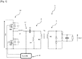
- the inverter 10 here makes it possible to chop an input voltage Vin (continuous) and thus to generate a square signal. If this square signal is at the right frequency, ie at the resonant frequency or at a frequency close to the resonant frequency of the pair Lr, Cr, the current can be considered purely sinusoidal for sufficiently high selectivity. The current then passes through the transformer T1 which provides galvanic isolation and is transmitted to an output load Rout via the secondary rectifier circuit 3.
- the first drawback is found at the level of the magnetic elements, that is to say at the level of the inductors and of the transformer, which are dimensioned for a precise operating frequency and which can cause losses in the case of operating frequencies far from their area of operation.
- An increase in reactive power in the cell can lead to an increase in currents (exchange of energy between the converter and the source) and therefore an increase in losses.
- the invention aims to overcome all or part of the problems mentioned above by proposing an innovative structure of a parallel series resonant power converter capable of extending its use over a wider operating range while guaranteeing good performance.
- the invention thus makes it possible to have a resonant power converter capable of operating for all loads and exhibiting high dynamics.
- the second half-bridge is in phase opposition to the first half-bridge for low load operation.
- Vin is the input voltage across the first half-bridge and the second half-bridge
- Lc is the inductance of the first and second inductors
- fdec is a chopping frequency of the resonant circuit, for low load operation.
- the first half-bridge comprises a first switch and a second switch
- the second half-bridge comprises a third switch and a fourth switch
- the first half-bridge and the second half-bridge being configured to be traversed by a current and generating a voltage
- the control means of the first half-bridge and of the second half-bridge are configured to delay the current with respect to the voltage, so as to obtain a smooth switching.
- Coss is the output capacity of the first, second, third, and fourth switches.
- the resonant circuit is an LC circuit.
- the resonant circuit is an LLC circuit.
- the second half-bridge is in phase with the first half-bridge for full load operation.
- in parallel means that the elements not belonging to the same branch are grouped by their end of the same polarity and work at the same time.
- in series means that the elements belong to the same current branch and work successively.
- antiparallel means that the elements are oriented parallel to each other, but traversed by a current in the opposite direction.
- the figure 1 which was presented previously, conventionally represents a power converter structure 1 known from the state of the art.
- the inverter 101 is provided by four switches Q1, Q2, Q3 and Q4.
- the switches Q1 and Q2 form a first half-bridge D1 and the switches Q3 and Q4 form a second half-bridge D2.
- the first half-bridge D1 is in parallel with the second half-bridge D2.
- a first inductance Lc1 is positioned in series with the first half-bridge D1 and connects the first half-bridge D1 and the resonant circuit LC.
- a second inductor Lc2 is positioned in series with the second half-bridge D2 and connects the second half-bridge D2 and the resonant circuit LC.
- the switches Q1, Q2, Q3 and Q4 can be transistors, as shown in figure 2 .
- the first inductance Lc1 and the second inductance Lc2 have the same inductance Lc and are coupled in the opposite direction to each other. That is to say that the first inductance Lc1 is in parallel with the second inductor Lc2 and that the second inductance Lc2 is crossed by a current in the opposite direction with respect to the current passing through the first inductor Lc1.
- first inductance Lc1 and the second inductance Lc2 are made on the same magnetic circuit, that is to say that the first inductance Lc1 and the second inductance Lc2 are crossed by the same flux produced by the signed sum currents flowing through the first inductance Lc1 and the second inductance Lc2.
- the first half-bridge D1 is in phase with the second half-bridge D2 and the first inductor Lc1 and the second inductor Lc2 are invisible to the power converter structure 100.
- the currents are opposite in the first inductance Lc1 and the second inductance Lc2, which induces that the flux produced at the level of the first inductor Lc1 and the second inductance Lc2 is zero and therefore that the first inductance Lc1 and the second inductance Lc2 are invisible to the structure of the power converter 100.
- the first half-bridge D1 and the second half-bridge D2 operate in phase opposition and the currents are opposite and equal.
- the current supplied to the load which is the sum of the currents is zero.
- the opposite currents produce a maximum flux in the first inductor Lc1 and the second inductor Lc2 and limit the current flowing between the first half-bridge D1 and the second half-bridge D2.
- the amplitude of this current is limited by the value of the inductance, chosen to ensure smooth switching, a phenomenon presented below.
- the control means 4 ensure the management of the two operations mentioned above and allow an intermediate operation between the two types of operation presented.
- the control means 4 are configured to adjust the phase difference between the first half-bridge D1 and the second half-bridge D2 to adjust the output voltage as a function of the load and of the input voltage.
- the control means 4 can, by way of example, ensure an intermediate operation based on a linear current management model between the two types of operation. To do this, the control means 4 detect the current at the output of the inverter 101 or the output voltage Vout and control the first half-bridge D1 and the second half-bridge D2 of the inverter 101 as a function of the detected current. .
- the management of the output load Rout of the power converter 100 is no longer done by means of the variation of the frequency and therefore by moving the operating frequency of the power converter 100 away from its resonant frequency but by the variation of the phase shift observed between the currents crossing the first half-bridge D1 and the second half-bridge D2 of the inverter 101.
- the power converter 100 as presented, then operates for all cases possible at or near the resonant frequency, frequencies which ensure efficient operation.
- the power converter structure 100 shown in figure 2 , according to the invention has advantages vis-à-vis soft switching. Indeed, the control means 4 of the inverter 101 are configured to delay the current with respect to the voltage, so as to obtain soft switching.
- the power converter structure 100 By extension with what has been said previously, thanks to the power converter structure 100 according to the invention, it is possible to work in soft switching over the entire load range of the power supply. This is an advantage, on the one hand to limit the losses in the switches Q1, Q2, Q3 and Q4, which therefore leads to improving the efficiency, and on the other hand, to limit the electromagnetic and electrical disturbances induced by the food. In this way, the invention makes it possible to reduce the size of the filters installed in the power converter 100.
- each switch Q1, Q2, Q3 and Q4 can have a diode (Di1 for Q1, Di2 for Q2, Di3 for Q3 and Di4 for Q4) in antiparallel to the switch and can have a capacitor (C1 for Q1, C2 for Q2, C3 for Q3 and C4 for Q4), in parallel.
- These capacitors C1, C2, C3 and C4 can be the parasitic capacitance of the switch or be those of an added capacitor as shown on the diagram. figure 2 . In this way, the power converter 100 can operate in soft switching (ZVS) and even no-load.
- the power converter 100 can be equipped with two transistors D5 and D6, in parallel with the secondary rectifier circuit 3, between the secondary rectifier circuit 3 and the output load Rout.
- figure 3 has further advantages of the power converter 100 structure.
- figure 3 schematically represents the inverter 101 of the structure of the power converter 100 according to the invention in the case of no-load operation where the currents are opposed in the first inductor Lc1 and the second inductor Lc2. More precisely, the figure 3 presents the first half-bridge D1, made up of switches Q1 and Q2 connected in series to the first inductor Lc1, in parallel with the second half-bridge D2, made up of switches Q3 and Q4 connected in series to the second inductor Lc2.
- a current Ic is measurable, between the first inductance Lc1 and the second inductance Lc2.
- the current Ic being dependent on the value of the first inductance Lc1 and on the value of the second inductance Lc2, it can be included in a current range I cpkpk .
- the current range I cpkpk extends around the standardized value of the current Ic as a function of the operation of the power converter 100.
- the dead time tm is defined as the minimum time allowing the discharge of the capacitors C1, C2, C3 and C4 and the re-engagement of the switches Q1, Q2, Q3 and Q4.
- the power converter 100 according to the invention makes it possible to make the dead time tm independent of the input voltage Vin , which simplifies the control of the switches Q1, Q2, Q3. and Q4.
- the idle time can be interpreted as the maximum time that can be set through low load or no-load operation. It is possible to decrease it during high load operation.
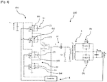
- This variant of the structure of the power converter 100 adds an inductance Lm in parallel with the transformer T1, which makes it possible to dissociate two resonances.
- the use of the inductance Lm in parallel with the transformer T1 makes it possible to reduce the magnetic inductance generated at the level of the transformer T1.
- the series resonant circuit then becomes an LLC circuit with two inductors Lr and Lm and a capacitor Cr.
- the first and second coupled inductors Lc1 Lc2 make it possible to limit the current exchanged between the first half-bridge D1 and the second half-bridge D2 when they are in phase opposition and to add the currents without impacting the power converter when they are in phase.
- the operation of the power supply takes place close to the resonant frequency.
- the capacitor Cr of the series resonant circuit can be separated into a first secondary capacitor Cr1 and a second secondary capacitor Cr2, as shown in figure 5 , each worth half of the initial capacitance of the capacitor Cr.
- the first secondary capacitor Cr1 is placed between the first half-bridge D1 and the first inductor Lc1 and, in the same way, the second secondary capacitor Cr2 is placed between the second half-bridge D2 and the second inductor Lc2.
Landscapes
- Engineering & Computer Science (AREA)
- Power Engineering (AREA)
- Dc-Dc Converters (AREA)
- Inverter Devices (AREA)
Abstract
Description
- Le domaine de l'invention est celui des convertisseurs de puissance résonants. La conversion de tension continue est utilisée dans de nombreux domaines technologiques allant de la nécessité à convertir la tension d'alimentation de dispositifs, tel que la conversion de la tension délivrée par une batterie d'ordinateur portable vers un processeur; à des applications évoluant dans des environnements beaucoup plus critiques tel que celui du spatial. L'invention trouve une utilité particulière dans le domaine du spatial mais peut être employée dans d'autres domaines qui demandent une flexibilité sur les charges à alimenter ou sur la tension d'entrée, notamment celui de l'automobile.
- De manière générale, la fonction d'un convertisseur de puissance en sa sortie est de fournir à la cible la tension et le courant nécessaire à son fonctionnement.
- Les convertisseurs à résonance sont conçus pour une plage de tension d'entrée et de courant de sortie données. Dans une structure résonante classique, le fonctionnement est assuré à la fréquence de résonance ou pour une fréquence proche. Dans ces conditions et pour une sélectivité suffisamment grande, le courant dans la structure est de forme sinusoïdale ou quasi-sinusoïdale.
- La variation de la tension d'entrée ou de la charge se fait souvent par une modification de la fréquence de fonctionnement de l'alimentation d'un convertisseur à résonance. Or la modification de la fréquence de fonctionnement affecte le rapport entre la puissance active et réactive et ne permet pas d'optimiser le rendement sur toute la plage de fonctionnement des convertisseurs à résonance.
- La modification de la fréquence de fonctionnement de l'alimentation d'un convertisseur à résonance rend également difficile le dimensionnement des éléments magnétiques et des filtres autour du convertisseur de puissance résonant.
- De plus, pour des plages de fonctionnement très étendues, il devient difficile d'assurer un fonctionnement efficient dans tous les cas d'utilisation.
- La
figure 1 représente une structure connue de l'art antérieur. Classiquement, un convertisseur de puissance 1 résonant comporte : - un onduleur 10 assuré par deux interrupteurs Qi1 et Qi2,
- un circuit résonant LC série avec une inductance Lr et un condensateur Cr,
- un transformateur T1 comprenant un circuit primaire 2 avec un enroulement de N1 spires et un circuit redresseur secondaire 3 avec un enroulement de N2 spires, qui permet de réaliser la fonction isolation galvanique,
- et des moyens 4 de contrôle de l'onduleur 10.
- L'onduleur 10 permet ici de hacher une tension d'entrée Vin (continue) et ainsi de générer un signal carré. Si ce signal carré est à la bonne fréquence, i.e. à la fréquence de résonance ou à une fréquence proche de la fréquence de résonnance du couple Lr, Cr, le courant peut être considéré purement sinusoïdal pour une sélectivité suffisamment grande. Le courant passe alors par le transformateur T1 qui permet l'isolation galvanique et est transmis à une charge de sortie Rout par l'intermédiaire du circuit redresseur secondaire 3.
- L'ajout d'une inductance Lm en parallèle du transformateur T1, comme représenté en
figure 1 , permet de dissocier deux résonances. Le fait de travailler entre ces deux résonances par modification de la fréquence rend possible la variation de charge de sortie Rout et l'adaptation aux variations de tensions d'entrée et de sortie. - Plus l'écart entre ces charges est grand, plus l'écart entre les gains requis est grand, et plus il est nécessaire de modifier la fréquence pour balayer la plage de tension de sortie Vout souhaitée. Ceci présente quatre inconvénients. Le premier inconvénient se retrouve au niveau des éléments magnétiques, c'est-à-dire au niveau des inductances et du transformateur, qui sont dimensionnés pour une fréquence de fonctionnement précise et qui peuvent occasionner des pertes dans le cas de fréquences de fonctionnement éloignées de leur zone de fonctionnement.
- Le second inconvénient se retrouve au niveau de la dynamique. Balayer une grande plage de fréquence implique une réduction de la dynamique du système.
- Une augmentation de la puissance réactive dans la cellule peut entrainer une augmentation des courants (échange d'énergie entre le convertisseur et la source) et donc une augmentation des pertes.
- Enfin, modifier la fréquence de fonctionnement peut entrainer des discontinuités sur le courant de sortie, augmentant la valeur du courant transmis au secondaire et augmentant donc les pertes.
- L'invention vise à pallier tout ou partie des problèmes cités plus haut en proposant une structure innovante de convertisseur de puissance résonant série parallèle capable d'étendre son utilisation sur une plage de fonctionnement plus large tout en garantissant de bonnes performances. L'invention permet ainsi de disposer d'un convertisseur de puissance résonant pouvant fonctionner pour toutes les charges et présentant une dynamique élevée.
- A cet effet, l'invention a pour objet un convertisseur de puissance à circuit résonant parallèle comportant :
- un onduleur,
- un circuit résonant,
- un transformateur comprenant un circuit primaire et un circuit secondaire,
- des moyens de contrôle de l'onduleur, l'onduleur étant relié au circuit résonant qui est destiné à être connecté à une charge de sortie à travers le transformateur, caractérisé en ce que l'onduleur comprend :
- un premier demi-pont et un second demi-pont en parallèle du premier demi-pont,
- une première inductance entre le premier demi-pont et le circuit résonant,
- une deuxième inductance entre le second demi-pont et le circuit résonant, et en ce que les première et deuxième inductances ont la même inductance et sont couplées en sens inverse l'une par rapport à l'autre.
- Selon un aspect de l'invention, le second demi-pont est en opposition de phase du premier demi-pont pour un fonctionnement à faible charge.
- Selon un aspect de l'invention, un courant Ic traversant les première et deuxième inductances est tel que :

- Où Vin est la tension d'entrée aux bornes du premier demi-pont et du second demi-pont, Lc est l'inductance des première et deuxième inductances et fdec est une fréquence de découpage du circuit résonant, pour un fonctionnement à faible charge.
- Selon un aspect de l'invention, le premier demi-pont comprend un premier interrupteur et un deuxième interrupteur, le second demi-pont comprend un troisième interrupteur et un quatrième interrupteur, le premier demi-pont et le second demi-pont étant configurés pour être traversés par un courant et générant une tension et les moyens de contrôle du premier demi-pont et du second demi-pont sont configurés pour retarder le courant par rapport à la tension, de manière à obtenir une commutation douce.
- Selon un aspect de l'invention, un temps mort tm défini comme le temps de décharge des premier condensateur de capacité C1, deuxième condensateur de capacité C2, troisième condensateur de capacité C3, quatrième condensateur de capacité C4 et de ré-enclenchement des premier interrupteur, deuxième interrupteur, troisième interrupteur et quatrième interrupteur est tel que :

- Où Coss est la capacité de sortie des premier, deuxième, troisième et quatrième interrupteurs.
- Selon un aspect de l'invention, le circuit résonant est un circuit LC.
- Selon un aspect de l'invention, le circuit résonant est un circuit LLC.
- Selon un aspect de l'invention, le second demi-pont est en phase du premier demi-pont pour un fonctionnement à pleine charge.
- L'invention sera mieux comprise et d'autres avantages apparaîtront à la lecture de la description détaillée d'un mode de réalisation donné à titre d'exemple, description illustrée par le dessin joint dans lequel :
- [
Fig.1 ] Lafigure 1 représente schématiquement une structure connue de l'art antérieur ; - [
Fig.2 ] Lafigure 2 représente schématiquement une structure de convertisseur de puissance selon l'invention ; - [
Fig.3 ] Lafigure 3 représente schématiquement l'onduleur de la structure du convertisseur de puissance selon l'invention ; - [
Fig.4 ] Lafigure 4 représente schématiquement une variante de la structure de convertisseur de puissance ; - [
Fig.5 ] Lafigure 5 représente schématiquement une autre variante de la structure de convertisseur de puissance. - Par souci de clarté, les mêmes éléments porteront les mêmes repères dans les différentes figures.
- Dans la présente description, le terme « en parallèle » signifie que les éléments n'appartenant pas à la même branche sont groupés par leur extrémité de même polarité et travaillent en même temps. Le terme « en série » signifie que les éléments appartiennent à une même branche de courant et travaillent successivement. Le terme « en antiparallèle » signifie que les éléments sont orientés parallèlement l'un à l'autre, mais parcourus par un courant dans le sens opposé.
- La
figure 1 , qui a été présentée précédemment, représente classiquement une structure de convertisseur de puissance 1 connue de l'état de l'art. - La
figure 2 représente schématiquement une structure d'un convertisseur de puissance 100 selon l'invention. Comme dans l'état de l'art, le convertisseur de puissance 100 comporte : - un onduleur 101 capable de hacher une tension d'entrée Vin et ainsi de générer un signal carré,
- un circuit résonant LC série avec une inductance Lr et un condensateur Cr relié à l'onduleur 101,
- un transformateur T1 comprenant un circuit primaire 2 avec un enroulement de N1 spires et un circuit redresseur secondaire 3 avec un enroulement de N2 et N3 spires, qui permet de réaliser la fonction isolation galvanique,
- et des moyens 4 de contrôle de l'onduleur 101.
- A la différence de l'état de l'art, l'onduleur 101 est assuré par quatre interrupteurs Q1, Q2, Q3 et Q4. Les interrupteurs Q1 et Q2 forment un premier demi-pont D1 et les interrupteurs Q3 et Q4 forment un second demi-pont D2. Le premier demi-pont D1 est en parallèle du second demi-pont D2. Une première inductance Lc1 est positionnée en série du premier demi-pont D1 et relie le premier demi pont D1 et le circuit résonant LC. Une deuxième inductance Lc2 est positionnée en série du second demi-pont D2 et relie le second demi pont D2 et le circuit résonant LC. De façon non limitative, les interrupteurs Q1, Q2, Q3 et Q4 peuvent être des transistors, comme représenté en
figure 2 . - Afin d'effectuer une gestion efficiente des courants transmis à la charge de sortie Rout, la première inductance Lc1 et la deuxième inductance Lc2 possède une même inductance Lc et sont couplées en sens inverse l'une par rapport à l'autre. C'est-à-dire que la première inductance Lc1 est en parallèle de la deuxième inductance Lc2 et que la deuxième inductance Lc2 est traversée par un courant dans le sens inverse par rapport au courant traversant la première inductance Lc1. Nous pouvons donc comprendre que la première inductance Lc1 et la deuxième inductance Lc2 sont réalisées sur le même circuit magnétique, c'est-à-dire que la première inductance Lc1 et la deuxième inductance Lc2 sont traversées par un même flux produit par la somme signée des courants qui traversent la première inductance Lc1 et la deuxième inductance Lc2.
- Ainsi, lors d'un fonctionnement à pleine charge, le premier demi-pont D1 est en phase avec le second demi-pont D2 et la première inductance Lc1 et la deuxième inductance Lc2 sont invisibles pour la structure de convertisseur de puissance 100. En effet, les courants sont opposés dans la première inductance Lc1 et la deuxième inductance Lc2, ce qui induit que le flux produit au niveau de la première inductance Lc1 et la deuxième inductance Lc2 est nul et donc que la première inductance Lc1 et la deuxième inductance Lc2 sont invisibles pour la structure du convertisseur de puissance 100.
- A l'inverse, lors d'un fonctionnement à faible charge, le premier demi-pont D1 et le second demi-pont D2 fonctionnent en opposition de phase et les courants sont opposés et égaux. Le courant fourni à la charge qui est la somme des courants est nul. Les courants opposés produisent un flux maximal dans la première inductance Lc1 et la deuxième inductance Lc2 et limite le courant qui circule entre le premier demi-pont D1 et le second demi-pont D2. L'amplitude de ce courant est limitée par la valeur de l'inductance, choisie pour assurer de la commutation douce, phénomène présenté ci-après.
- Les moyens de contrôle 4 assurent la gestion des deux fonctionnements cités précédemment et permettent un fonctionnement intermédiaire entre les deux types de fonctionnement présentés. Les moyens de contrôle 4 sont configurés pour ajuster la différence de phase entre le premier demi-pont D1 et le second demi-pont D2 pour ajuster la tension de sortie en fonction de la charge et de la tension d'entrée. Les moyens de contrôle 4 peuvent, à titre d'exemple, assurer un fonctionnement intermédiaire basé sur un modèle de gestion linéaire du courant entre les deux types de fonctionnement. Pour ce faire, les moyens de contrôle 4 détectent le courant en sortie de l'onduleur 101 ou la tension de sortie Vout et commandent le premier demi-pont D1 et le second demi-pont D2 de l'onduleur 101 en fonction du courant détecté.
- De cette manière, la gestion de la charge de sortie Rout du convertisseur de puissance 100 ne se fait plus à l'aide de la variation de la fréquence et donc en éloignant la fréquence de fonctionnement du convertisseur de puissance 100 vis-à-vis de sa fréquence de résonance mais par la variation du déphasage observé entre les courants traversant le premier demi-pont D1 et le second demi-pont D2 de l'onduleur 101. Le convertisseur de puissance 100, tel que présenté, fonctionne alors pour tous les cas éventuels à la fréquence de résonance ou à proximité de la fréquence de résonance, fréquences qui assurent un fonctionnement efficient.
- Un autre inconvénient de l'état de l'art présenté en
figure 1 est la gestion des pertes. En effet, avec l'augmentation de la fréquence de fonctionnement des alimentations et l'éloignement du fonctionnement à proximité de la fréquence de résonnance, une partie du courant qui circule dans le circuit résonant n'est pas transmis à la charge et créé de la puissance réactive. Or, plus le fonctionnement est éloigné de la fréquence de résonnance, plus les pertes dans les interrupteurs et surtout dans les éléments magnétiques, augmentent. - A l'inverse de la commutation dure, lorsque le courant ou la tension dans l'interrupteur est nul ou que ces deux composantes sont opposées, la puissance dans l'interrupteur est nulle. Cette situation présente l'avantage de ne générer qu'une quantité faible de perte par commutation dans l'interrupteur, du fait de l'absence de puissance à dissiper. L'énergie emmagasinée dans les capacités parasites des interrupteurs circule alors, permettant la mise en conduction sans perte de ceux-ci on parle de « soft switching » ou commutation douce. A l'inverse, lorsque le courant et la tension dans un interrupteur sont non nuls, une puissance est dissipée dans l'interrupteur. On parle alors de commutation dure ou « hard-switching ».
- Lorsque la tension est nulle lors d'une commutation, l'homme du métier parle de « commutation à zéro de tension » (ZVS), et identiquement « commutation à zéro de courant » lorsque le courant est nul (ZCS). Généralement, ce phénomène est appelé commutation douce ou « soft switching ».
- La structure de convertisseur de puissance 100, présentée en
figure 2 , selon l'invention présente des avantages vis-à-vis de la commutation douce. En effet, les moyens de contrôle 4 de l'onduleur 101 sont configurés pour retarder le courant par rapport à la tension, de manière à obtenir une commutation douce. - Par extension avec ce qui a été dit précédemment, grâce à la structure de convertisseur de puissance 100 selon l'invention, il est possible de travailler en commutation douce sur toute la plage de charge de l'alimentation. Ceci est un avantage, d'une part pour limiter les pertes dans les interrupteurs Q1, Q2, Q3 et Q4, ce qui induit donc d'améliorer le rendement, et d'autre part, limiter les perturbations électromagnétiques et électriques induites par l'alimentation. De cette manière, l'invention permet de réduire la taille des filtres implantés dans le convertisseur de puissance 100.
- En outre, chaque interrupteur Q1, Q2, Q3 et Q4 peut présenter une diode (Di1 pour Q1, Di2 pour Q2, Di3 pour Q3 et Di4 pour Q4) en antiparallèle à l'interrupteur et peut présenter une capacité (C1 pour Q1, C2 pour Q2, C3 pour Q3 et C4 pour Q4), en parallèle. Ces capacités C1, C2, C3 et C4 peuvent être la capacité parasite de l'interrupteur ou être celles d'un condensateur ajouté comme montré sur la
figure 2 . De cette manière, le convertisseur de puissance 100 peut fonctionner en commutation douce (ZVS) et même à vide. - De plus, le convertisseur de puissance 100 peut être équipé de deux transistors D5 et D6, en parallèle du circuit redresseur secondaire 3, entre le circuit redresseur secondaire 3 et la charge de sortie Rout.
- La
figure 3 présente d'autres avantages de la structure de convertisseur de puissance 100. Lafigure 3 représente schématiquement l'onduleur 101 de la structure du convertisseur de puissance 100 selon l'invention dans le cas d'un fonctionnement à vide où les courants sont opposés dans la première inductance Lc1 et la deuxième inductance Lc2. Plus précisément, lafigure 3 présente le premier demi-pont D1, composé des interrupteurs Q1 et Q2 reliés en série à la première inductance Lc1, en parallèle du second demi-pont D2, composé des interrupteurs Q3 et Q4 reliés en série à la deuxième inductance Lc2. - De cette manière, un courant Ic est mesurable, entre la première inductance Lc1 et la deuxième inductance Lc2. Le courant Ic est directement lié à la valeur de la première inductance Lc1, à la valeur de la deuxième inductance Lc2 et à la tension d'entrée Vin à travers l'équation suivante :

où Lc est la valeur de la première inductance Lc1 et de la deuxième inductance Lc2, Vin est la valeur de la tension d'entrée et fdec est la fréquence d'utilisation du convertisseur de puissance 100 ou fréquence de découpage. - Cette formule est valable lors du fonctionnement à vide, lorsque les courants sont en opposition de phase dans les première et deuxième inductances Lc1 Lc2 couplées telle qu'illustrée par la
figure 3 . - De plus, le courant Ic étant dépendant de la valeur de la première inductance Lc1 et de la valeur de la deuxième inductance Lc2, il peut être compris dans une plage de courant Icpkpk. La plage de courant Icpkpk s'étend autour de la valeur normée du courant Ic en fonction du fonctionnement du convertisseur de puissance 100.
- Un autre avantage de la structure du convertisseur de puissance 100 selon l'invention est la gestion d'un temps mort tm qui est le temps nécessaire à la mise en place d'une commutation douce. Plus précisément, le temps mort tm est défini comme le temps minimum permettant la décharge des capacités C1, C2, C3 et C4 et le ré-enclenchement des interrupteurs Q1, Q2, Q3 et Q4. En effet, le convertisseur de puissance 100 selon l'invention permet de rendre le temps mort tm indépendant de la tension d'entrée Vin ce qui simplifie la commande des interrupteurs Q1, Q2, Q3 et Q4. Ainsi, le temps mort tm peut être défini pour tous les fonctionnements en fonction des capacités de sorties COSS des interrupteurs Q1, Q2, Q3 et Q4 comme :

- Le temps mort peut être interprété comme le temps maximum qui peut être fixé grâce au fonctionnement à faible charge ou à vide. Il est possible de le diminuer lors d'un fonctionnement à forte charge.
- La
figure 4 représente schématiquement une variante de la structure de convertisseur de puissance 100. Comme présenté enfigure 2 , le convertisseur de puissance 100 comporte : - un onduleur 101, assuré par les quatre interrupteurs Q1, Q2, Q3 et Q4, les interrupteurs Q1 et Q2 formant le premier demi-pont D1 et les interrupteurs Q3 et Q4 formant le second demi-pont D2, capable de hacher une tension d'entrée Vin et ainsi de générer un signal carré,
- un circuit résonant série relié à l'onduleur 101,
- un transformateur T1 comprenant un circuit primaire 2 avec un enroulement de N1 spires et un circuit redresseur secondaire 3 avec un enroulement de N2 et N3 spires, qui permet de réaliser la fonction isolation galvanique,
- et des moyens 4 de contrôle de l'onduleur 101.
- Cette variante de la structure du convertisseur de puissance 100 ajoute une inductance Lm en parallèle du transformateur T1, ce qui permet de dissocier deux résonances. L'utilisation de l'inductance Lm en parallèle du transformateur T1 permet de réduire l'inductance magnétique générée au niveau du transformateur T1. Le circuit résonant série devient alors un circuit LLC avec deux inductances Lr et Lm et un condensateur Cr.
- Les premières et deuxièmes inductances Lc1 Lc2 couplées permettent de limiter le courant échangé entre le premier demi-pont D1 et le second demi-pont D2 lorsqu'ils sont en opposition de phase et d'additionner les courants sans impacter le convertisseur de puissance lorsqu'ils sont en phase.
- De manière avantageuse, le fonctionnement de l'alimentation se fait à proximité de la fréquence de résonnance.
- Le condensateur Cr du circuit résonant série peut être séparée en une première capacité secondaire Cr1 et une deuxième capacité secondaire Cr2, comme représenté en
figure 5 , valant chacune la moitié de la capacité initiale du condensateur Cr. La première capacité secondaire Cr1 est placée entre le premier demi-pont D1 et la première inductance Lc1 et, de la même manière, la deuxième capacité secondaire Cr2 est placée entre le deuxième demi-pont D2 et la deuxième inductance Lc2. Cette configuration rend le système insensible aux dissymétries sur la commande.
Claims (5)
- Convertisseur de puissance (100) à circuit résonant parallèle comportant :- Un onduleur (101),- Un circuit résonant (LC),- Un transformateur (T1) comprenant un circuit primaire (2) et un circuit secondaire (3),- Des moyens de contrôle (4) de l'onduleur (101), l'onduleur (101) étant relié au circuit résonant (LC) qui est destiné à être connecté à une charge de sortie (Rout) à travers le transformateur (T1),caractérisé en ce que le convertisseur de puissance (100) comprend une inductance Lm en parallèle du transformateur (T1) et en ce que l'onduleur (101) comprend :- un premier demi-pont (D1) et un second demi-pont (D2) en parallèle du premier demi-pont (D1),- une première inductance (Lc1) entre le premier demi-pont (D1) et le circuit résonant (LC),- une deuxième inductance (Lc2) entre le second demi-pont (D2) et le circuit résonant (LC),et en ce que les première et deuxième inductances (Lc1, Lc2) ont la même inductance et sont couplées en sens inverse l'une par rapport à l'autre.
- Convertisseur de puissance (100) selon la revendication 1, dans lequel le second demi-pont (D2) est en opposition de phase du premier demi-pont (D1) pour un fonctionnement à faible charge et dans lequel un courant Ic traversant les première et deuxième inductances (Lc1, Lc2) est tel que :

- Convertisseur de puissance (100) selon la revendication 2, dans lequel le premier demi-pont (D1) comprend un premier interrupteur (Q1) et un deuxième interrupteur (Q2), le second demi-pont (D2) comprend un troisième interrupteur (Q3) et un quatrième interrupteur (Q4), le premier demi-pont (D1) et le second demi-pont (D2) étant configurés pour être traversés par un courant et générant une tension et les moyens de contrôle (4) du premier demi-pont (D1) et du second demi-pont (D2) sont configurés pour retarder le courant par rapport à la tension, de manière à obtenir une commutation douce (ZVS).
- Convertisseur de puissance (100) selon la revendication 3, dans lequel le premier interrupteur (Q1) comporte un premier condensateur de capacité C1, le deuxième interrupteur (Q2) comporte un deuxième condensateur de capacité C2, le troisième interrupteur (Q3) comporte un troisième condensateur de capacité C3, le quatrième interrupteur (Q4) comporte un quatrième condensateur de capacité C4 et dans lequel un temps mort tm défini comme le temps de décharge des premier condensateur de capacité C1, deuxième condensateur de capacité C2, troisième condensateur de capacité C3, quatrième condensateur de capacité C4 et de ré-enclenchement des premier interrupteur (Q1), deuxième interrupteur (Q2), troisième interrupteur (Q3) et quatrième interrupteur (Q4) est tel que :

- Convertisseur de puissance (100) selon la revendication 1, dans lequel le second demi-pont (D2) est en phase du premier demi-pont (D1) pour un fonctionnement à pleine charge.
Applications Claiming Priority (1)
| Application Number | Priority Date | Filing Date | Title |
|---|---|---|---|
| FR2006217A FR3111491A1 (fr) | 2020-06-15 | 2020-06-15 | Convertisseur de puissance résonant |
Publications (1)
| Publication Number | Publication Date |
|---|---|
| EP3926809A1 true EP3926809A1 (fr) | 2021-12-22 |
Family
ID=72885661
Family Applications (1)
| Application Number | Title | Priority Date | Filing Date |
|---|---|---|---|
| EP21177462.5A Withdrawn EP3926809A1 (fr) | 2020-06-15 | 2021-06-02 | Convertisseur de puissance resonant |
Country Status (8)
| Country | Link |
|---|---|
| US (1) | US11594972B2 (fr) |
| EP (1) | EP3926809A1 (fr) |
| JP (1) | JP7798487B2 (fr) |
| CN (1) | CN113809922A (fr) |
| BR (1) | BR102021010726A2 (fr) |
| CA (1) | CA3122390A1 (fr) |
| FR (1) | FR3111491A1 (fr) |
| TW (1) | TWI904166B (fr) |
Families Citing this family (8)
| Publication number | Priority date | Publication date | Assignee | Title |
|---|---|---|---|---|
| EP3796537B1 (fr) * | 2019-09-20 | 2022-04-20 | Hitachi Energy Switzerland AG | Cellule de convertisseur à double pont actif comportant un inducteur de transfert d'énergie divisé pour un équilibrage optimisé du courant dans le transformateur moyenne fréquence (mft) |
| US11742764B2 (en) * | 2021-02-04 | 2023-08-29 | Maxim Integrated Products, Inc. | Resonant power converters including coupled inductors |
| TWI822432B (zh) * | 2022-04-13 | 2023-11-11 | 立錡科技股份有限公司 | 功率轉換器及其控制方法 |
| TWI826090B (zh) * | 2022-04-19 | 2023-12-11 | 立錡科技股份有限公司 | 功率轉換器及其控制方法 |
| CN117277766A (zh) * | 2022-04-27 | 2023-12-22 | 郭青山 | 一种零电压开关半桥电源转换电路和电器 |
| CN115664246B (zh) * | 2022-12-12 | 2023-04-07 | 惠州市乐亿通科技有限公司 | 多相逆变电路及调制方法 |
| CN116915045A (zh) * | 2023-07-13 | 2023-10-20 | 捷蒽迪电子科技(上海)有限公司 | 一种非隔离llc谐振变换器 |
| CN117997084B (zh) * | 2024-04-07 | 2024-07-12 | 广东高斯宝电气技术有限公司 | 一种用于提高llc拓扑效率的sr死区控制方法 |
Citations (3)
| Publication number | Priority date | Publication date | Assignee | Title |
|---|---|---|---|---|
| US6246599B1 (en) * | 2000-08-25 | 2001-06-12 | Delta Electronics, Inc. | Constant frequency resonant inverters with a pair of resonant inductors |
| US6392902B1 (en) * | 2000-08-31 | 2002-05-21 | Delta Electronics, Inc. | Soft-switched full-bridge converter |
| CN107241020A (zh) * | 2017-07-03 | 2017-10-10 | 杭州中恒电气股份有限公司 | 谐振直流/直流变换器 |
Family Cites Families (4)
| Publication number | Priority date | Publication date | Assignee | Title |
|---|---|---|---|---|
| US8901897B2 (en) * | 2012-03-02 | 2014-12-02 | International Business Machines Corporation | Operating a DC-DC converter |
| EP2903146B1 (fr) * | 2014-02-03 | 2019-03-20 | STMicroelectronics Srl | Convertisseur résonant monophasé ou polyphasé avec commande de rétroaction |
| JP2018174648A (ja) | 2017-03-31 | 2018-11-08 | オムロン株式会社 | Llc共振コンバータ |
| US10199947B2 (en) * | 2017-04-05 | 2019-02-05 | Futurewei Technologies, Inc. | Isolated partial power processing power converters |
-
2020
- 2020-06-15 FR FR2006217A patent/FR3111491A1/fr active Pending
-
2021
- 2021-05-25 JP JP2021087380A patent/JP7798487B2/ja active Active
- 2021-05-27 TW TW110119224A patent/TWI904166B/zh active
- 2021-06-02 EP EP21177462.5A patent/EP3926809A1/fr not_active Withdrawn
- 2021-06-02 BR BR102021010726-0A patent/BR102021010726A2/pt unknown
- 2021-06-08 US US17/342,487 patent/US11594972B2/en active Active
- 2021-06-11 CN CN202110652367.1A patent/CN113809922A/zh active Pending
- 2021-06-15 CA CA3122390A patent/CA3122390A1/fr active Pending
Patent Citations (3)
| Publication number | Priority date | Publication date | Assignee | Title |
|---|---|---|---|---|
| US6246599B1 (en) * | 2000-08-25 | 2001-06-12 | Delta Electronics, Inc. | Constant frequency resonant inverters with a pair of resonant inductors |
| US6392902B1 (en) * | 2000-08-31 | 2002-05-21 | Delta Electronics, Inc. | Soft-switched full-bridge converter |
| CN107241020A (zh) * | 2017-07-03 | 2017-10-10 | 杭州中恒电气股份有限公司 | 谐振直流/直流变换器 |
Non-Patent Citations (1)
| Title |
|---|
| . .: "AN-4151 Half-Bridge LLC Resonant Converter Design Using FSFR-Series Fairchild Power Switch (FPS(TM))", 22 October 2014 (2014-10-22), pages 1 - 18, XP055847071, Retrieved from the Internet <URL:https://s1.dtsheet.com/store/data/001360852.pdf?key=e76d7fac9933d24bd61dd103e1a56839&r=1> [retrieved on 20211004] * |
Also Published As
| Publication number | Publication date |
|---|---|
| US20210391801A1 (en) | 2021-12-16 |
| TWI904166B (zh) | 2025-11-11 |
| JP7798487B2 (ja) | 2026-01-14 |
| CN113809922A (zh) | 2021-12-17 |
| CA3122390A1 (fr) | 2021-12-15 |
| JP2021197904A (ja) | 2021-12-27 |
| BR102021010726A2 (pt) | 2021-12-21 |
| US11594972B2 (en) | 2023-02-28 |
| KR20210155359A (ko) | 2021-12-22 |
| TW202201887A (zh) | 2022-01-01 |
| FR3111491A1 (fr) | 2021-12-17 |
Similar Documents
| Publication | Publication Date | Title |
|---|---|---|
| EP3926809A1 (fr) | Convertisseur de puissance resonant | |
| EP3940943B1 (fr) | Convertisseur de résonance isolé et son procédé de commande | |
| JP6019770B2 (ja) | 双方向絶縁型dc−dcコンバータの制御装置 | |
| JP2011526478A (ja) | 共振型電力コンバータ | |
| JPH04355505A (ja) | E級固定周波数変換器 | |
| FR2891417A1 (fr) | Convertisseur de courant continu a resonance serie | |
| CN103036405A (zh) | 一种移相全桥电路的同步整流开关管驱动方法及装置 | |
| CN112087140B (zh) | 一种多模式自动切换的两级谐振dc-dc转换器 | |
| EP3207629B1 (fr) | Convertisseur dc/dc isole | |
| EP3529897B1 (fr) | Dispositif de commande d'un transistor | |
| EP3373429A1 (fr) | Convertisseur à double pont et procédé de commande d'un tel convertisseur | |
| CN102468764A (zh) | 谐振式转换器的调节增益方法及其装置 | |
| Ye et al. | A low-ripple high-frequency high-voltage power supply for ion pumps | |
| EP3687051B1 (fr) | Convertisseur resonant serie parallele llcc | |
| FR3129543A1 (fr) | Procede de commande d’un convertisseur de tension | |
| RU2830228C2 (ru) | Резонансный преобразователь мощности | |
| Maleki et al. | A Non‐Isolated High Step‐Up DC–DC Converter Based on Switched Capacitor and Quadratic Cell With Reduced Voltage Stress on Semiconductors | |
| KR102959127B1 (ko) | 공진 전력 변환기 | |
| NL9300860A (nl) | Stuurschakeling voor fasegemoduleerde brug omzetter. | |
| FR3073343A1 (fr) | Convertisseur de puissance a tres haute frequence de commutation | |
| FR3103655A1 (fr) | Module de commutation et convertisseur de puissance comportant un tel module | |
| HK40055465A (en) | Resonant power converter | |
| CN100508350C (zh) | 串联谐振电路及实现其空载稳压的方法 | |
| EP4732416A1 (fr) | Convertisseur électrique continu-continu isolé, réseau électrique comprenant un tel convertisseur électrique et procédé de conversion associé | |
| Sha et al. | Optimal design of circuit parameters of DAB converter based on cascaded bidirectional converters |
Legal Events
| Date | Code | Title | Description |
|---|---|---|---|
| PUAI | Public reference made under article 153(3) epc to a published international application that has entered the european phase |
Free format text: ORIGINAL CODE: 0009012 |
|
| STAA | Information on the status of an ep patent application or granted ep patent |
Free format text: STATUS: THE APPLICATION HAS BEEN PUBLISHED |
|
| AK | Designated contracting states |
Kind code of ref document: A1 Designated state(s): AL AT BE BG CH CY CZ DE DK EE ES FI FR GB GR HR HU IE IS IT LI LT LU LV MC MK MT NL NO PL PT RO RS SE SI SK SM TR |
|
| B565 | Issuance of search results under rule 164(2) epc |
Effective date: 20211012 |
|
| STAA | Information on the status of an ep patent application or granted ep patent |
Free format text: STATUS: REQUEST FOR EXAMINATION WAS MADE |
|
| 17P | Request for examination filed |
Effective date: 20220620 |
|
| RBV | Designated contracting states (corrected) |
Designated state(s): AL AT BE BG CH CY CZ DE DK EE ES FI FR GB GR HR HU IE IS IT LI LT LU LV MC MK MT NL NO PL PT RO RS SE SI SK SM TR |
|
| STAA | Information on the status of an ep patent application or granted ep patent |
Free format text: STATUS: EXAMINATION IS IN PROGRESS |
|
| 17Q | First examination report despatched |
Effective date: 20221202 |
|
| P01 | Opt-out of the competence of the unified patent court (upc) registered |
Effective date: 20230529 |
|
| STAA | Information on the status of an ep patent application or granted ep patent |
Free format text: STATUS: THE APPLICATION IS DEEMED TO BE WITHDRAWN |
|
| 18D | Application deemed to be withdrawn |
Effective date: 20230613 |