EP3929594A1 - Verfahren zur herstellung einer vorrichtung zur messung von stromstärken und vorrichtung zur messung von stromstärken - Google Patents
Verfahren zur herstellung einer vorrichtung zur messung von stromstärken und vorrichtung zur messung von stromstärken Download PDFInfo
- Publication number
- EP3929594A1 EP3929594A1 EP21000135.0A EP21000135A EP3929594A1 EP 3929594 A1 EP3929594 A1 EP 3929594A1 EP 21000135 A EP21000135 A EP 21000135A EP 3929594 A1 EP3929594 A1 EP 3929594A1
- Authority
- EP
- European Patent Office
- Prior art keywords
- circuit board
- contact pin
- resistor arrangement
- connection
- connection elements
- Prior art date
- Legal status (The legal status is an assumption and is not a legal conclusion. Google has not performed a legal analysis and makes no representation as to the accuracy of the status listed.)
- Granted
Links
Images


Classifications
-
- G—PHYSICS
- G01—MEASURING; TESTING
- G01R—MEASURING ELECTRIC VARIABLES; MEASURING MAGNETIC VARIABLES
- G01R1/00—Details of instruments or arrangements of the types included in groups G01R5/00 - G01R13/00 and G01R31/00
- G01R1/20—Modifications of basic electric elements for use in electric measuring instruments; Structural combinations of such elements with such instruments
- G01R1/203—Resistors used for electric measuring, e.g. decade resistors standards, resistors for comparators, series resistors, shunts
-
- G—PHYSICS
- G01—MEASURING; TESTING
- G01R—MEASURING ELECTRIC VARIABLES; MEASURING MAGNETIC VARIABLES
- G01R19/00—Arrangements for measuring currents or voltages or for indicating presence or sign thereof
-
- G—PHYSICS
- G01—MEASURING; TESTING
- G01R—MEASURING ELECTRIC VARIABLES; MEASURING MAGNETIC VARIABLES
- G01R1/00—Details of instruments or arrangements of the types included in groups G01R5/00 - G01R13/00 and G01R31/00
- G01R1/02—General constructional details
- G01R1/04—Housings; Supporting members; Arrangements of terminals
- G01R1/0408—Test fixtures or contact fields; Connectors or connecting adaptors; Test clips; Test sockets
- G01R1/0416—Connectors, terminals
-
- G—PHYSICS
- G01—MEASURING; TESTING
- G01R—MEASURING ELECTRIC VARIABLES; MEASURING MAGNETIC VARIABLES
- G01R1/00—Details of instruments or arrangements of the types included in groups G01R5/00 - G01R13/00 and G01R31/00
- G01R1/02—General constructional details
- G01R1/06—Measuring leads; Measuring probes
- G01R1/067—Measuring probes
- G01R1/06711—Probe needles; Cantilever beams; "Bump" contacts; Replaceable probe pins
- G01R1/06733—Geometry aspects
-
- G—PHYSICS
- G01—MEASURING; TESTING
- G01R—MEASURING ELECTRIC VARIABLES; MEASURING MAGNETIC VARIABLES
- G01R1/00—Details of instruments or arrangements of the types included in groups G01R5/00 - G01R13/00 and G01R31/00
- G01R1/02—General constructional details
- G01R1/06—Measuring leads; Measuring probes
- G01R1/067—Measuring probes
- G01R1/06711—Probe needles; Cantilever beams; "Bump" contacts; Replaceable probe pins
- G01R1/06755—Material aspects
- G01R1/06761—Material aspects related to layers
-
- G—PHYSICS
- G01—MEASURING; TESTING
- G01R—MEASURING ELECTRIC VARIABLES; MEASURING MAGNETIC VARIABLES
- G01R15/00—Details of measuring arrangements of the types provided for in groups G01R17/00 - G01R29/00, G01R33/00 - G01R33/26 or G01R35/00
- G01R15/14—Adaptations providing voltage or current isolation, e.g. for high-voltage or high-current networks
- G01R15/146—Measuring arrangements for current not covered by other subgroups of G01R15/14, e.g. using current dividers, shunts, or measuring a voltage drop
-
- G—PHYSICS
- G01—MEASURING; TESTING
- G01R—MEASURING ELECTRIC VARIABLES; MEASURING MAGNETIC VARIABLES
- G01R19/00—Arrangements for measuring currents or voltages or for indicating presence or sign thereof
- G01R19/0092—Measuring current only
-
- G—PHYSICS
- G01—MEASURING; TESTING
- G01R—MEASURING ELECTRIC VARIABLES; MEASURING MAGNETIC VARIABLES
- G01R27/00—Arrangements for measuring resistance, reactance, impedance, or electric characteristics derived therefrom
- G01R27/02—Measuring real or complex resistance, reactance, impedance, or other two-pole characteristics derived therefrom, e.g. time constant
-
- G—PHYSICS
- G01—MEASURING; TESTING
- G01R—MEASURING ELECTRIC VARIABLES; MEASURING MAGNETIC VARIABLES
- G01R3/00—Apparatus or processes specially adapted for the manufacture or maintenance of measuring instruments, e.g. of probe tips
-
- G—PHYSICS
- G01—MEASURING; TESTING
- G01R—MEASURING ELECTRIC VARIABLES; MEASURING MAGNETIC VARIABLES
- G01R31/00—Arrangements for testing electric properties; Arrangements for locating electric faults; Arrangements for electrical testing characterised by what is being tested not provided for elsewhere
- G01R31/28—Testing of electronic circuits, e.g. by signal tracer
- G01R31/2801—Testing of printed circuits, backplanes, motherboards, hybrid circuits or carriers for multichip packages [MCP]
- G01R31/2806—Apparatus therefor, e.g. test stations, drivers, analysers, conveyors
- G01R31/2808—Holding, conveying or contacting devices, e.g. test adapters, edge connectors, extender boards
-
- H—ELECTRICITY
- H01—ELECTRIC ELEMENTS
- H01C—RESISTORS
- H01C17/00—Apparatus or processes specially adapted for manufacturing resistors
- H01C17/02—Apparatus or processes specially adapted for manufacturing resistors adapted for manufacturing resistors with envelope or housing
-
- H—ELECTRICITY
- H01—ELECTRIC ELEMENTS
- H01C—RESISTORS
- H01C17/00—Apparatus or processes specially adapted for manufacturing resistors
- H01C17/28—Apparatus or processes specially adapted for manufacturing resistors adapted for applying terminals
-
- H—ELECTRICITY
- H05—ELECTRIC TECHNIQUES NOT OTHERWISE PROVIDED FOR
- H05K—PRINTED CIRCUITS; CASINGS OR CONSTRUCTIONAL DETAILS OF ELECTRIC APPARATUS; MANUFACTURE OF ASSEMBLAGES OF ELECTRICAL COMPONENTS
- H05K3/00—Apparatus or processes for manufacturing printed circuits
- H05K3/30—Assembling printed circuits with electric components, e.g. with resistors
- H05K3/306—Assembling printed circuits with electric components, e.g. with resistors with lead-in-hole components
- H05K3/308—Adaptations of leads
-
- H—ELECTRICITY
- H01—ELECTRIC ELEMENTS
- H01C—RESISTORS
- H01C1/00—Details
- H01C1/14—Terminals or tapping points specially adapted for resistors; Arrangements of terminals or tapping points on resistors
-
- H—ELECTRICITY
- H01—ELECTRIC ELEMENTS
- H01C—RESISTORS
- H01C1/00—Details
- H01C1/16—Resistor networks not otherwise provided for
Definitions
- the invention relates to a method for producing a device for measuring current intensities and to such a device.
- Measuring resistors connected in series with the component to be monitored are used to measure the current in electronic circuits.
- the current intensity is determined from the voltage drop across the measuring resistor, known as the shunt resistor.
- the correct and reliable measurement of the current is particularly important in a battery management system of an electric or hybrid vehicle, for example.
- a resistor arrangement which comprises such a low-resistance measuring resistor with approximately 10 to 50 ⁇ Ohm as well as connection elements for connecting the resistor arrangement to the circuit can be produced from a longitudinally welded composite material. This is for example from the publication EP 0 605 800 A1 known.
- the composite material is made from three metal strips by connecting the individual metal strips to one another via a longitudinal seam using an electron beam or laser welding process.
- the voltage drop across a measuring resistor is transmitted via contact pins or similar elements, which are arranged on both sides of the measuring resistor on the connection elements, are tapped. Such contact pins can be soldered, pressed or welded onto the connection elements of the resistor arrangement.
- the voltage is recorded and processed by measuring and evaluation electronics.
- electronic components are provided that can be arranged on a circuit board. The circuit board can be located in the immediate vicinity of the resistor arrangement.
- connection contacts are provided for tapping the voltage, which are formed by stamping and threading in the plate-shaped sections that are used to connect the resistor arrangement to the external circuit.
- the connection of the measuring lines for voltage measurement to the connection contacts is made by means of cable lugs and fastening screws.
- the invention is based on the object of specifying an improved, in particular simpler and more cost-effective method for producing a device for measuring current intensities and such a device.
- the measurement of current strengths is also understood to mean the measurement of the strength of an electrical current that may change over time.
- the resistor arrangement described above can comprise a low-ohmic shunt resistor as a resistor element.
- the connection elements of the resistor arrangement can be made of copper, a preferably low-alloy copper alloy, aluminum or a preferably low-alloy aluminum alloy, or comprise at least one of these materials.
- the resistance element may be made of a copper alloy which is commonly used as a resistance alloy.
- the specific electrical resistance of the resistance alloy is significantly greater than the specific electrical resistance of the material of the connection elements.
- the connection elements can be terminal connection elements of the resistor arrangement. However, it is also possible for at least one connection element to be arranged between two resistance elements in relation to a possible current path.
- the resistor arrangement can be formed in a planar arrangement.
- the connection elements and the at least one resistance element are formed as plate-shaped or strip-shaped elements and are arranged in a plane next to one another, preferably in a row.
- the thickness of the resistance element or the resistance elements can be arbitrary. Usually, however, it is not greater than the thickness of the connection elements.
- the circuit board has at least one conductor track, which is preferably arranged on the side of the circuit board facing away from the resistor arrangement. Furthermore, electrical components can be arranged on the circuit board, which are used for measuring and evaluating electrical signals. With the term Through hole is a recess in the circuit board that extends over the entire thickness of the circuit board.
- a contact pin is understood to mean a material protrusion that rises above the otherwise undeformed surface of a connection element.
- the contact pin is shaped by displacing the material of a connection element essentially in the direction perpendicular to the surface of the connection element.
- the direction in which the material is displaced defines the axis of the contact pin.
- the contact pin can be solid, partially hollow or hollow along its entire axis.
- the cross-sectional shape of the contact pin can be arbitrary, preferably circular, rectangular, square or hexagonal in the case of a solid contact pin or ring-shaped in the case of a hollow contact pin.
- the shape and / or size of the cross section of the contact pin can be constant or change continuously or discontinuously along the extension of the contact pin.
- a contact pin can have a slightly conical contour, that is to say a contour with boundary surfaces that are slightly inclined in relation to the surface of the connection element.
- the contact pin can have a shoulder.
- a shoulder is understood to be a discontinuous, that is to say abrupt change in the cross-sectional shape and / or the cross-sectional size of the contact pin.
- the height of the contact pin in relation to the undeformed surface of the connection element is greater than the thickness of the circuit board.
- the contact pin can, preferably together with a further contact pin, be used as a voltage tap for measuring the electrical voltage dropping across at least one resistance element.
- the contact pin can also be used to ground the resistor arrangement.
- One or more of the connection elements of the resistor arrangement are preferred shaped such contact pins.
- the contact pins, which are used for voltage measurement, are positioned as close as possible to the resistance element on which the voltage drop is to be determined.
- the lateral widening of the contact pin in method step d) denotes a deformation of the contact pin by displacing material perpendicular to the axis of the contact pin, that is, a radial displacement - based on the axis. This deformation takes place to a greater extent in the area of the contact pin that protrudes beyond the circuit board. In this area, the lateral extent of the displaced material according to method step d) is at least locally larger than the width of the through hole.
- the lateral widening of its section protruding beyond the printed circuit board allows the contact pin to have a shape similar to that of a mushroom or a nail in the area of the nail head.
- the cross section of the contact pin in the axial direction can in particular be T-shaped.
- the lateral widening of the contact pin also takes place in the area that is located within the through-hole of the circuit board. In this area, the lateral widening is limited by the inner wall of the through hole.
- connection pin is molded directly from the material of a connection element, it is not necessary to mount it separately on the resistor arrangement or on the circuit board. The work steps and materials required for this, such as solder, are no longer required. Multiple contact pins can be molded at the same time. The monolithic connection between The connection element and contact pin avoid undesired contact stresses that can falsify a measurement.
- the contact pins can be formed at the same time as the composite material is being cut to length. In this case, steps a) and b) of the method are carried out simultaneously. A separate, additional work step for shaping the contact pins is therefore not necessary. The method is thus faster and more cost-effective than if the contact pins are only formed after the composite material has been cut to length. Furthermore, a high positional accuracy of the contact pins is achieved in this way.
- the contact pin can be shaped in process step b) by an embossing step or by extrusion.
- Embossing and extrusion are particularly suitable for forming contact pins that are monolithically connected to the material of the connection elements and that extend essentially perpendicular to the surface of the connection elements.
- the material is shaped using a stamp.
- a negative mold with at least one recess corresponding to the contour of the contact pin can be used to shape the contact pin.
- the outer contour of the contact pin can be determined by such a negative shape.
- the lateral widening of the contact pin in method step d) can be carried out by an upsetting process, by embossing, by caulking or by Flanging take place.
- Flanging is preferably used for a contact pin that is hollow along its entire axis, while the other methods are preferably used for a solid or only partially hollow contact pin. With this method, the force that is necessary for lateral deformation is introduced in the direction of the axis of the contact pin.
- the material of the contact pin is not only widened laterally, but also pressed onto the circuit board in the direction of its axis.
- the methods mentioned are particularly suitable for widening the part of the contact pin protruding beyond the circuit board in all or only in certain directions perpendicular to the axis of the contact pin and at the same time achieving good mechanical fixation of the circuit board on the resistor arrangement.
- the lateral widening of the contact pin in method step d) can be supported by heating the material by means of ultrasound or by means of a laser.
- the material of the contact pin is very solidified and hard due to the deformation in process step b). This is a hindrance for the subsequent deformation in step d).
- the material of the contact pin can be heated to such an extent that it is at least partially softened, that is to say becomes softer. The deformation in step d) is then more easily possible.
- the electrically conductive connection can advantageously be established in method step e) by laterally widening the contact pin in the region of its protrusion in method step d). By deforming the contact pin in step d), a non-positive connection is established between the circuit board and the contact pin. It is advantageously also provided that the widened area of the contact pin comes into contact with at least one conductor track that is located on the surface of the circuit board facing away from the resistor arrangement. the Frictional connection between the circuit board and the contact pin then also leads to an electrical connection between the contact pin and the conductor track.
- the electrically conductive connection can be established in method step e) by deforming the contact pin in such a way that it contacts the inner surface of the through-hole in the circuit board.
- the inner surface of the through hole has an electrically conductive material that is connected to at least one conductor track on the circuit board.
- the lateral widening of the contact pin in step d) results in a non-positive connection between the contact pin and the inside of the through-hole, for example in the manner of a press fit. In this way, a particularly good electrical contact can be established between the contact pin and the conductor track.
- the device comprises a resistor arrangement and a printed circuit board mechanically and electrically connected to the resistor arrangement.
- the resistor arrangement comprises at least two connection elements and at least one resistance element arranged between the connection elements in relation to the direction of current flow, the at least one resistance element on the one hand and the connection elements on the other made of different, electrical conductive materials.
- the circuit board has at least one through hole. Furthermore, the circuit board has at least one conductor track, which is preferably arranged on the side of the circuit board facing away from the resistor arrangement.
- the resistor arrangement has at least one contact pin monolithically connected to one of the connection elements and machined from the material of the connection element, through which the resistor arrangement is connected to the circuit board by the contact pin extending through the through-hole in the circuit board, protruding beyond it and has a lateral widening on the side of the circuit board facing away from the resistor arrangement, by means of which the circuit board is mechanically fixed on the resistor arrangement.
- connection element prevents undesired contact stresses which can falsify a measurement.
- device can be manufactured inexpensively and with high precision, because the contact pin is molded directly from the material of the connection element.
- the at least one contact pin can be in electrical contact with at least one conductor track of the circuit board by means of its lateral widening. The mechanical fixation of the circuit board on the resistor arrangement and the electrical contacting of these components then take place through the contact pin.
- the at least one contact pin can be in electrical contact with the inner surface of the through-hole in the circuit board.
- the at least one contact pin can have a shoulder on which the circuit board rests in such a way that the circuit board is spaced from the connection element and thus from the resistor arrangement.
- the distance between the circuit board and the resistor arrangement results in better thermal decoupling of the circuit board from the resistor arrangement.
- the heat that arises when current flows through the resistor element cannot be transferred directly from the resistor element or from a connection element to the circuit board, but the heat must flow through the contact pin.
- the contact pin Due to its relatively small cross-section, the contact pin represents a high thermal resistance. The heat flow from the resistor arrangement to the circuit board is therefore reduced and the circuit board remains at a lower temperature level than if the circuit board were to rest directly on a connection element.
- This embodiment is particularly advantageous when the thickness of the resistance element is not less than the thickness of the connection elements.
- the surface of the at least one contact pin can have a metallic coating, in particular a coating containing tin, silver or nickel.
- a metallic coating prevents corrosion and can thus ensure that the electrical contact between the contact pin and the conductor track is of high quality over the entire service life of the device.
- the coating can have been applied before the contact pin was formed in step b) or the contact pin can be coated in a separate step between method steps b) and c) have been.
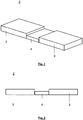
- Fig. 1 shows an oblique view of a resistor arrangement 2 without a contact pin.
- the resistor arrangement 2 has two terminal connection elements 3 and a resistance element 4 which is positioned between the two connection elements 3.
- the connection elements 3 and the resistance element 4 each have a plate-like shape.
- the thickness of the resistor element 4 is somewhat less than the thickness of the two connection elements 3.
- the resistor arrangement 2 can be connected to a circuit at the two connection elements 3.
- the two connection elements 3 can have connecting devices (not shown), for example bores. These connection devices are each attached in the region of the connection elements 3 which is remote from the resistance element 4.
- the resistance element 4 is located between the connection elements 3 in relation to the direction of current flow. When a current flows, an electrical voltage drops across the resistance element 4, on the basis of which the strength of the current flowing through the resistance arrangement 2 can be determined.
- Fig. 2 shows a side view of a resistor arrangement 2 according to Fig. 1 .
- a resistor arrangement 2 as in Figures 1 and 2 shown can be produced in a known manner by longitudinal seam welding of three strips to form a composite material and then cutting the welded composite material to length.
- Fig. 3 shows the resistor arrangement 2 according to FIG Figs. 1 and 2 upon completion of process step b).
- a negative mold 12 with two recesses 13 was positioned on the top of the resistor arrangement 2.
- two stamps 11 have penetrated the material of the two connection elements 3.
- the punches 11 are positioned in such a way that they are opposite the recesses 13 of the negative mold 12.
- material of the connection elements 3 was displaced perpendicular to the surface of the connection elements 3 and shifted into the recesses 13 of the negative mold 12. In this way, two material projections were formed, which form contact pins 5.
- the contact pins 5 are solid in the illustrated case.
- Fig. 4 shows the resistor arrangement 2 with two shaped contact pins 5 according to method step b).
- the stamps 11 and the negative mold 12 have been removed.
- the The punch 11 and the recesses 13 in the negative mold 12 each have a contour with bevels for removal from the mold.
- the shaped contact pins 5 can also have a contour with bevels.
- the angle that the bevels enclose with the normal to the surface of the connection elements 3 for removal from the mold is typically approximately 2 °. Because of this slight deviation from the normal, the bevels are not explicitly shown in the figures.
- the height of the contact pins 5 is marked with the symbol H.
- the contact pins 5 are provided for tapping the electrical voltage dropping across the resistance element 4. In order to minimize falsification of the measured value, the contact pins 5 were formed from the connection elements 3 in such a way that they are positioned close to the connection point between the respective connection element 3 and the resistance element 4.
- Fig. 5 shows the resistor arrangement 2 with two shaped contact pins 5 and a printed circuit board 8 positioned on the resistor arrangement 2.
- Fig. 5 thus represents the resistor arrangement 2 and the circuit board 8 according to method step c).
- the circuit board 8 has two through bores 9.
- the circuit board 8 was positioned in such a way that the contact pins 5 protrude through the through bores 9.
- the height H of the contact pins 5 is greater than the thickness T of the circuit board 8, so that the contact pins 5 each have a protrusion 6 over the circuit board 8 on the side of the circuit board 8 facing away from the resistor arrangement 2.
- the clear width of the through bores 9 is slightly larger than the outer dimension of the contact pins 5.
- Fig. 6 shows a device 1 for measuring current intensities with a resistor arrangement 2 and a printed circuit board 8 fixed on the resistor arrangement 2
- Fig. 6 shows the device 1 after method step e).
- the two contact pins 5 of the resistor arrangement 2 have been deformed in such a way that they mechanically fix the circuit board 8 on the resistor arrangement 2 and at the same time each form an electrical contact with a respective conductor track of the circuit board 8.
- the contact pins 5 were widened laterally both in the area of their protrusion 6 over the circuit board 8 and in the area which is located within the through-hole 9 of the circuit board 8. In the area of the through hole 9, the lateral widening is limited by the inner wall of the through hole 9.
- the contact pins 5 fill the respective through hole 9 in a form-fitting manner.
- the deformation takes place to such an extent that a lateral widening 7 is formed which extends further than the width of the respective through hole 9.
- the contact pins 5 are thus given a shape with a T-shaped cross section in the axial direction.
- the printed circuit board 8 is fixed in a force-fit manner on the resistor arrangement 2.
- the lateral widening 7 of each contact pin 5 makes contact with at least one conductor track on the side of the printed circuit board 8 facing away from the resistor arrangement 2. Electrical connections are thus established between the resistor arrangement 2 and the printed circuit board 8.
- the conductor tracks are connected to electronic components, not shown, by means of which the voltage drop across the resistance element 4 can be determined.
- FIG. 1 shows a further exemplary embodiment of a device 1 for measuring current intensities with a resistor arrangement 2 and a printed circuit board 8 fixed on the resistor arrangement 2 Fig. 7
- the thickness of the resistance element 4 is approximately equal to the thickness of the connection elements 3.
- the contact pins 5 each have a shoulder 51 which runs around the contact pin 5 and on which the printed circuit board 8 rests.
- the contact pins 5 are designed in such a way that the outer dimensions of the contact pins 5 in the sub-area of the respective contact pin 5 that directly adjoins a connection element 3 are each greater than the clear width of the respective through-hole 9 of the circuit board 8.
- the circuit board 8 is neither directly on the connection elements 3 nor on the Resistance element 4, but rather it is at a distance s from the connection elements 3, from the resistance element 4 and thus from the entire resistor arrangement 2.
- the circuit board is thus thermally better decoupled from the resistor arrangement.
- FIG. 1 shows, as a further exemplary embodiment, a device 1 for measuring current intensities with a resistor arrangement 2 and a printed circuit board 8 fixed on the resistor arrangement 2, the contact pins 5 each being designed to be hollow over their entire extent.
- the contact pins 5 were crimped in the area of their protrusion 7.
- the contact pins 5 have a shape similar to that of a hollow rivet.
- the in Fig. 8 The illustrated embodiment of the device 1, the circuit board 8 rests on the two connection elements 3.
- resistor arrangements 2 which each comprise only one resistor element 4 and two terminal connection elements 3. It is also possible to apply the method described above to resistor arrangements which have two or more resistor elements 4 and at least one further connection element 3 arranged between two resistor elements 4 in relation to a possible current path.
- the resistor arrangement can be like this be configured that the same current flows through at least two resistance elements 4, which enables redundant current measurement, or that different currents flow through at least two resistance elements 4, which enables partial currents to be measured.
Landscapes
- Physics & Mathematics (AREA)
- General Physics & Mathematics (AREA)
- Engineering & Computer Science (AREA)
- Microelectronics & Electronic Packaging (AREA)
- Manufacturing & Machinery (AREA)
- Geometry (AREA)
- Computer Hardware Design (AREA)
- General Engineering & Computer Science (AREA)
- Measuring Instrument Details And Bridges, And Automatic Balancing Devices (AREA)
- Multi-Conductor Connections (AREA)
Abstract
Description
- Die Erfindung betrifft ein Verfahren zur Herstellung einer Vorrichtung zur Messung von Stromstärken und eine solche Vorrichtung.
- Für die Strommessung in elektronischen Schaltungen werden Messwiderstände verwendet, die in Reihe zu dem zu überwachenden Bauteil geschaltet sind. Dabei wird die Stromstärke aus der über den als Shunt-Widerstand bezeichneten Messwiderstand abfallenden Spannung bestimmt. Die korrekte und verlässliche Messung der Stromstärke ist beispielsweise besonders wichtig in einem Batteriemanagementsystem eines Elektro- oder Hybridfahrzeugs. Eine Widerstandsanordnung, die einen solchen niederohmigen Messwiderstand mit ungefähr 10 bis 50 µOhm sowie Anschlusselemente zum Verbinden der Widerstandsanordnung mit dem Stromkreis umfasst, kann aus einem längsnahtgeschweißten Verbundmaterial hergestellt werden. Dies ist beispielsweise aus der Druckschrift
EP 0 605 800 A1 bekannt. Das Verbundmaterial wird aus drei Metallbändern hergestellt, indem die einzelnen Metallbänder jeweils über eine Längsnaht miteinander durch ein Elektronenstrahl- oder Laserschweißverfahren verbunden werden. - Die über einem Messwiderstand abfallende Spannung wird über Kontaktstifte oder ähnliche Elemente, die beidseitig vom Messwiderstand auf den Anschlusselementen angeordnet sind, abgegriffen. Solche Kontaktstifte können auf den Anschlusselementen der Widerstandsanordnung aufgelötet, aufgepresst oder aufgeschweißt sein. Die Spannung wird von einer Mess- und Auswerteelektronik erfasst und weiterverarbeitet. Hierfür sind elektronische Bauteile vorgesehen, die auf einer Leiterplatte angeordnet sein können. Die Leiterplatte kann sich dabei in unmittelbarer Nähe der Widerstandsanordnung befinden.
- Aus der Druckschrift
DE 10 2009 031 408 A1 ist eine Widerstandsanordnung mit einem niederohmigen Strommesswiderstand bekannt. Bei dieser Widerstandsanordnung sind zum Abgriff der Spannung Anschlusskontakte vorgesehen, die durch Ausprägung und Gewindeformung in den plattenförmigen Teilstücken, die zum Anschluss der Widerstandsanordnung an den äußeren Stromkreis dienen, gebildet sind. Der Anschluss der Messleitungen zur Spannungsmessung an die Anschlusskontakte erfolgt mittels Kabelschuhen und Befestigungsschrauben. - Des Weiteren ist aus der Druckschrift
US 10 163 553 B2 - Bei den aus dem Stand der Technik bekannten Vorrichtungen ist es notwendig, zusätzliche Bauteile zu verwenden, um die über dem Messwiderstand abfallende Spannung abzugreifen. Dies erfordert zusätzlichen Aufwand und Kosten. Ferner können an den Kontaktstellen der einzelnen Bauteile Kontaktspannungen auftreten, die das Spannungssignal verfälschen können.
- Der Erfindung liegt die Aufgabe zugrunde, ein verbessertes, insbesondere einfacheres und kostengünstigeres Verfahren zur Herstellung einer Vorrichtung zur Messung von Stromstärken und eine solche Vorrichtung anzugeben.
- Die Erfindung wird bezüglich eines Verfahrens durch die Merkmale des Anspruchs 1 und bezüglich einer Vorrichtung durch die Merkmale des Anspruchs 8 wiedergegeben. Die weiteren, rückbezogenen Ansprüche betreffen vorteilhafte Aus- und Weiterbildungen der Erfindung.
- Die Erfindung schließt ein Verfahren zur Herstellung einer Vorrichtung zur Messung von Stromstärken mittels einer Widerstandsanordnung ein, wobei das Verfahren folgende Schritte umfasst:
- a) Bereitstellen einer Widerstandsanordnung umfassend mindestens zwei Anschlusselemente und mindestens ein in Bezug auf die Richtung des Stromflusses zwischen den Anschlusselementen angeordnetes Widerstandselement, wobei das mindestens eine Widerstandselement einerseits und die Anschlusselemente andererseits aus unterschiedlichen, elektrisch leitenden Materialien bestehen,
- b) Formen mindestens eines Kontaktstifts aus dem Material mindestens eines Anschlusselements,
- c) Positionieren einer Leiterplatte, welche mindestens eine Leiterbahn und mindestens eine Durchgangsbohrung aufweist, auf der Widerstandsanordnung derart, dass der mindestens eine Kontaktstift durch die Durchgangsbohrung hindurch ragt und auf der der Widerstandsanordnung abgewandten Seite der Leiterplatte einen Überstand über die Leiterplatte aufweist,
- d) Laterales Verbreitern des Kontaktstifts zumindest im Bereich seines Überstands durch Verformung des Materials, so dass die Leiterplatte auf der Widerstandsanordnung mechanisch fixiert wird,
- e) Herstellen einer elektrisch leitenden Verbindung zwischen dem Kontaktstift und mindestens einer Leiterbahn der Leiterplatte.
- Unter der Messung von Stromstärken wird auch die Messung der Stärke eines zeitlich sich möglicherweise verändernden elektrischen Stroms verstanden. Die vorstehend beschriebene Widerstandsanordnung kann einen niederohmigen Shunt-Widerstand als Widerstandselement umfassen. Die Anschlusselemente der Widerstandsanordnung können aus Kupfer, einer bevorzugt niedriglegierten Kupferlegierung, aus Aluminium oder einer bevorzugt niedriglegierten Aluminiumlegierung sein oder mindestens einen dieser Werkstoffe umfassen. Das Widerstandselement kann aus einer Kupferlegierung sein, die als Widerstandslegierung üblicherweise verwendet wird. Der spezifische elektrische Widerstand der Widerstandslegierung ist deutlich größer als der spezifische elektrische Widerstand des Materials der Anschlusselemente. Die Anschlusselemente können endständige Anschlusselemente der Widerstandsanordnung sein. Es ist aber auch möglich, dass mindestens ein Anschlusselement in Bezug auf einen möglichen Strompfad zwischen zwei Widerstandselementen angeordnet ist. Die Widerstandsanordnung kann in planarer Anordnung ausgebildet sein. Dabei sind die Anschlusselemente und das mindestens eine Widerstandselement als platten- oder streifenförmige Elemente gebildet und in einer Ebene nebeneinander, bevorzugt in einer Reihe, angeordnet. Die Dicke des Widerstandselements beziehungsweise der Widerstandselemente kann dabei beliebig sein. Üblicherweise ist sie aber nicht größer als die Dicke der Anschlusselemente.
- Die Leiterplatte weist mindestens eine Leiterbahn auf, die bevorzugt auf der von der Widerstandanordnung abgewandten Seite der Leiterplatte angeordnet ist. Ferner können auf der Leiterplatte elektrische Bauteile angeordnet sein, die zur Messung und Auswertung von elektrischen Signalen dienen. Mit dem Begriff Durchgangsbohrung wird eine Aussparung in der Leiterplatte bezeichnet, die sich über die gesamte Dicke der Leiterplatte erstreckt.
- Unter Kontaktstift wird ein Werkstoffvorsprung verstanden, der sich über die sonst unverformte Oberfläche eines Anschlusselements erhebt. Das Formen des Kontaktstifts erfolgt durch Verlagern von Material eines Anschlusselements im Wesentlichen in Richtung senkrecht zur Oberfläche des Anschlusselements. Die Richtung, in der das Material verlagert wird, definiert die Achse des Kontaktstifts. Der Kontaktstift kann massiv, teilweise hohl oder entlang seiner gesamten Achse hohl sein. Die Querschnittsform des Kontaktstifts kann beliebig sein, bevorzugt kreisförmig, rechteckig, quadratisch oder sechseckig bei einem massiven Kontaktstift oder ringförmig bei einem hohlen Kontaktstift. Form und/oder Größe des Querschnitts des Kontaktstifts können konstant sein oder sich entlang der Erstreckung des Kontaktstifts stetig oder unstetig verändern. Beispielsweise kann ein Kontaktstift eine leicht konische Kontur, also eine Kontur mit bezogen auf die Oberfläche des Anschlusselements leicht geneigten Begrenzungsflächen aufweisen. Ferner kann der Kontaktstift einen Absatz aufweisen. Unter einem Absatz wird eine unstetige, also sprungartige Veränderung der Querschnittsform und/oder der Querschnittsgröße des Kontaktstifts verstanden. Die Höhe des Kontaktstifts bezogen auf die unverformte Oberfläche des Anschlusselements ist größer als die Dicke der Leiterplatte. Folglich weist der Kontaktstift einen Überstand über die Leiterplatte auf, wenn die Leiterplatte so auf der Widerstandsanordnung positioniert wird, dass der Kontaktstift durch die Durchgangsbohrung hindurch und über sie hinaus ragt.
- Der Kontaktstift kann, bevorzugt zusammen mit einem weiteren Kontaktstift, als Spannungsabgriff zur Messung der über mindestens einem Widerstandselement abfallenden elektrischen Spannung verwendet werden. Alternativ kann der Kontaktstift auch zur Erdung der Widerstandsanordnung dienen. Bevorzugt werden in allen Anschlusselementen der Widerstandsanordnung ein oder mehrere solcher Kontaktstifte geformt. Dabei werden die Kontaktstifte, die zur Spannungsmessung dienen, möglichst nahe an dem Widerstandselement positioniert, an dem der Spannungsabfall ermittelt werden soll.
- Das laterale Verbreitern des Kontaktstifts in Verfahrensschritt d) bezeichnet ein Verformen des Kontaktstifts durch Verlagern von Material senkrecht zur Achse des Kontaktstifts, also ein - bezogen auf die Achse - radiales Verlagern. Dieses Verformen erfolgt in größerer Ausprägung im dem Bereich des Kontaktstifts, der über die Leiterplatte hinausragt. In diesem Bereich ist die laterale Erstreckung des verlagerten Materials nach Verfahrensschritt d) zumindest lokal größer als die Weite der Durchgangsbohrung. Durch ein solches Verformen des Kontaktstifts wird die Leiterplatte auf der Widerstandsanordnung fixiert. Insbesondere kann der Kontaktstift durch das laterale Verbreitern seines über die Leiterplatte überstehenden Abschnitts eine Form ähnlich der eines Pilzes oder eines Nagels im Bereich des Nagelkopfes erhalten. Der Querschnitt des Kontaktstifts in axialer Richtung kann insbesondere T-förmig sein.
- In geringerer Ausprägung erfolgt das laterale Verbreitern des Kontaktstifts auch in dem Bereich, der sich innerhalb der Durchgangsbohrung der Leiterplatte befindet. In diesem Bereich wird die laterale Verbreiterung durch die Innenwand der Durchgangsbohrung begrenzt.
- Der besondere Vorteil des beschriebenen Verfahrens besteht darin, dass zur Herstellung der Verbindung zwischen Widerstandsanordnung und Leiterplatte keine zusätzlichen Bauteile und/oder Materialien benötigt werden. Weil der Kontaktstift direkt aus dem Material eines Anschlusselements geformt wird, ist es nicht erforderlich, ihn separat auf der Widerstandsanordnung oder auf der Leiterplatte zu montieren. Es entfallen die hierfür notwendigen Arbeitsschritte und die benötigten Materialien, wie beispielsweise Lot. Mehrere Kontaktstifte können gleichzeitig geformt werden. Durch die monolithische Verbindung zwischen Anschlusselement und Kontaktstift werden unerwünschte Kontaktspannungen, die eine Messung verfälschen können, vermieden.
- Wird die Widerstandsanordnung hergestellt, indem sie aus einem längsnahtgeschweißten, bandförmigen Verbundmaterial abgelängt wird, dann können die Kontaktstifte gleichzeitig mit dem Ablängen des Verbundmaterials geformt werden. Die Schritte a) und b) des Verfahrens erfolgen in diesem Fall also gleichzeitig. Ein separater, zusätzlicher Arbeitsschritt für das Formen der Kontaktstifte ist somit nicht notwendig. Das Verfahren wird somit schneller und kostengünstiger als wenn die Kontaktstifte erst nach dem Ablängen des Verbundmaterials geformt werden. Ferner wird auf diese Weise eine hohe Positionsgenauigkeit der Kontaktstifte erreicht.
- Im Rahmen einer bevorzugten Ausführungsform der Erfindung kann das Formen des Kontaktstifts in Verfahrensschritt b) durch einen Prägeschritt oder durch Fließpressen erfolgen. Prägen und Fließpressen eignen sich besonders zur Formung von monolithisch mit dem Material der Anschlusselemente verbundenen Kontaktstiften, die sich im Wesentlichen senkrecht zur Oberfläche der Anschlusselemente erstrecken. Das Formen des Materials erfolgt dabei mittels eines Stempels.
- Im Rahmen einer speziellen Ausgestaltung dieser Ausführungsform der Erfindung kann zur Formgebung des Kontaktstifts eine Negativform mit mindestens einer der Kontur des Kontaktstifts entsprechenden Aussparung verwendet werden. Durch eine solche Negativform kann die äußere Kontur des Kontaktstifts bestimmt werden.
- Im Rahmen einer weiteren bevorzugten Ausführungsform der Erfindung kann das laterale Verbreitern des Kontaktstifts in Verfahrensschritt d) durch einen Stauchvorgang, durch Prägen, durch Verstemmen (caulking) oder durch Umbördeln (flanging) erfolgen. Umbördeln kommt dabei bevorzugt bei einem entlang seiner gesamten Achse hohlen Kontaktstift zur Anwendung, während die anderen Verfahren bei einem massiven oder nur teilweise hohlen Kontaktstift bevorzugt verwendet werden. Bei diesen Verfahren wird die Kraft, die zur lateralen Verformung notwendig ist, in Richtung der Achse des Kontaktstifts eingeleitet. Somit wird das Material des Kontaktstifts nicht nur lateral verbreitert, sondern auch in Richtung seiner Achse auf die Leiterplatte gepresst. Deshalb eignen sich die genannten Verfahren besonders gut, den über die Leiterplatte hinaus ragenden Teil des Kontaktstifts in alle oder nur in bestimmte Richtungen senkrecht zur Achse des Kontaktstifts zu verbreitern und gleichzeitig eine gute mechanische Fixierung der Leiterplatte auf der Widerstandsanordnung zu erzielen.
- Im Rahmen einer speziellen Ausgestaltung der Erfindung kann das laterale Verbreitern des Kontaktstifts in Verfahrensschritt d) durch Erwärmen des Materials mittels Ultraschall oder mittels eines Lasers unterstützt werden. Das Material des Kontaktstifts ist aufgrund der Verformung in Verfahrensschritt b) sehr verfestigt und hart. Dies ist für die nachfolgende Verformung in Schritt d) hinderlich. Durch den Eintrag von Wärme mittels eines Lasers oder mittels Ultraschall kann das Material des Kontaktstifts soweit erwärmt werden, dass es sich zumindest teilweise entfestigt, also weicher wird. Das Verformen in Schritt d) ist dann leichter möglich.
- Vorteilhafterweise kann das Herstellen der elektrisch leitenden Verbindung in Verfahrensschritt e) durch das laterale Verbreitern des Kontaktstifts im Bereich seines Überstands in Verfahrensschritt d) erfolgen. Durch das Verformen des Kontaktstifts in Schritt d) wird eine kraftschlüssige Verbindung zwischen der Leiterplatte und dem Kontaktstift hergestellt. Dabei ist vorteilhafterweise ferner vorgesehen, dass der verbreiterte Bereich des Kontaktstifts in Kontakt mit mindestens einer Leiterbahn kommt, die sich auf der von der Widerstandsanordnung abgewandten Oberfläche der Leiterplatte befindet. Die kraftschlüssige Verbindung zwischen der Leiterplatte und dem Kontaktstift führt dann auch zu einer elektrischen Verbindung zwischen dem Kontaktstift und der Leiterbahn.
- Im Rahmen einer zusätzlichen Ausführungsform der Erfindung kann das Herstellen der elektrisch leitenden Verbindung in Verfahrensschritt e) erfolgen, indem der Kontaktstift derart verformt wird, dass er die Innenoberfläche der Durchgangsbohrung der Leiterplatte kontaktiert. Hierbei weist die Innenoberfläche der Durchgangsbohrung ein elektrisch leitendes Material auf, das mit mindestens einer Leiterbahn der Leiterplatte in Verbindung steht. Durch das laterale Verbreitern des Kontaktstifts in Schritt d) kommt es zu einer kraftschlüssigen Verbindung zwischen dem Kontaktstift und der Innenseite der Durchgangsbohrung, beispielsweise in der Art einer Presspassung. Auf diese Weise kann ein besonders guter elektrischer Kontakt zwischen dem Kontaktstift und der Leiterbahn hergestellt werden.
- Hinsichtlich weiterer technischer Merkmale und Vorteile des erfindungsgemäßen Verfahrens wird hiermit explizit auf die nachstehenden Erläuterungen im Zusammenhang mit der erfindungsgemäßen Vorrichtung sowie auf die Figuren und die Figurenbeschreibung verwiesen.
- Ein weiterer Aspekt der Erfindung schließt eine Vorrichtung zur Messung von Stromstärken ein. Hierunter wird auch die Messung der Stärke eines zeitlich sich möglicherweise verändernden elektrischen Stroms verstanden. Die Vorrichtung umfasst eine Widerstandsanordnung und eine mit der Widerstandsanordnung mechanisch und elektrisch verbundene Leiterplatte. Die Widerstandsanordnung umfasst mindestens zwei Anschlusselemente und mindestens ein in Bezug auf die Richtung des Stromflusses zwischen den Anschlusselementen angeordnetes Widerstandselement, wobei das mindestens eine Widerstandselement einerseits und die Anschlusselemente andererseits aus unterschiedlichen, elektrisch leitenden Materialien bestehen. Die Leiterplatte weist mindestens eine Durchgangsbohrung auf. Ferner weist die Leiterplatte mindestens eine Leiterbahn auf, die bevorzugt auf der von der Widerstandsanordnung abgewandten Seite der Leiterplatte angeordnet ist. Gemäß der Erfindung weist die Widerstandsanordnung mindestens einen monolithisch mit einem der Anschlusselemente verbundenen und aus dem Material des Anschlusselements herausgearbeiteten Kontaktstift auf, durch den die Widerstandsanordnung mit der Leiterplatte verbunden ist, indem sich der Kontaktstift durch die Durchgangsbohrung der Leiterplatte hindurch erstreckt, über sie hinaus ragt und auf der von der Widerstandsanordnung abgewandten Seite der Leiterplatte eine laterale Verbreiterung aufweist, durch welche die Leiterplatte auf der Widerstandsanordnung mechanisch fixiert ist.
- Hinsichtlich der zur Beschreibung der Vorrichtung verwendeten Begriffe wird hiermit explizit auf die vorstehenden Erläuterungen der Begriffe im Zusammenhang mit der Beschreibung des Verfahrens zur Herstellung einer solchen Vorrichtung verwiesen.
- Der besondere Vorteil der beschriebenen Vorrichtung besteht darin, dass durch die monolithische Verbindung zwischen Anschlusselement und Kontaktstift unerwünschte Kontaktspannungen, die eine Messung verfälschen können, vermieden werden. Ferner kann die Vorrichtung kostengünstig und mit hoher Präzision hergestellt werden, denn der Kontaktstift ist unmittelbar aus dem Material des Anschlusselements herausgeformt.
- Im Rahmen einer Ausführungsform der Vorrichtung kann der mindestens eine Kontaktstift mittels seiner lateralen Verbreiterung in elektrischem Kontakt mit mindestens einer Leiterbahn der Leiterplatte stehen. Die mechanische Fixierung der Leiterplatte auf der Widerstandsanordnung und die elektrische Kontaktierung dieser Komponenten erfolgen dann durch den Kontaktstift.
- Im Rahmen einer weiteren Ausführungsform der Vorrichtung kann der mindestens eine Kontaktstift in elektrischem Kontakt mit der Innenoberfläche der Durchgangsbohrung der Leiterplatte stehen.
- Im Rahmen einer weiteren vorteilhaften Ausführungsform der Vorrichtung kann der mindestens eine Kontaktstift einen Absatz aufweisen, auf dem die Leiterplatte in einer Weise aufliegt, dass die Leiterplatte von dem Anschlusselement und somit von der Widerstandsanordnung beabstandet ist. Der Abstand zwischen der Leiterplatte und der Widerstandsanordnung bewirkt eine bessere thermische Entkopplung der Leiterplatte von der Widerstandsanordnung. Die Wärme, die bei Stromdurchfluss durch das Widerstandselement entsteht, kann in diesem Fall nicht direkt vom Widerstandselement oder von einem Anschlusselement auf die Leiterplatte übertragen werden, sondern die Wärme muss durch den Kontaktstift strömen. Aufgrund seines relativ kleinen Querschnitts stellt der Kontaktstift einen großen Wärmewiderstand dar. Der Wärmestrom von der Widerstandsanordnung zur Leiterplatte wird deshalb reduziert und die Leiterplatte bleibt auf einem niedrigeren Temperaturniveau als wenn die Leiterplatte direkt auf einem Anschlusselement aufliegen würde. Diese Ausführungsform ist besonders dann vorteilhaft, wenn die Dicke des Widerstandselements nicht kleiner als die Dicke der Anschlusselemente ist.
- In vorteilhafter Ausgestaltung der Erfindung kann die Oberfläche des mindestens einen Kontaktstifts eine metallische Beschichtung, insbesondere eine zinn-, silber- oder nickelhaltige Beschichtung, aufweisen. Eine solche Beschichtung verhindert Korrosion und kann somit dafür sorgen, dass der elektrische Kontakt zwischen dem Kontaktstift und der Leiterbahn über die gesamte Lebensdauer der Vorrichtung von hoher Güte ist. Die Beschichtung kann dabei vor dem Formen des Kontaktstifts in Schritt b) aufgebracht worden sein oder der Kontaktstift kann in einem separaten Schritt zwischen den Verfahrensschritten b) und c) beschichtet worden sein.
- Hinsichtlich weiterer technischer Merkmale und Vorteile der erfindungsgemäßen Vorrichtung wird hiermit explizit auf die Erläuterungen im Zusammenhang mit dem vorstehend beschriebenen erfindungsgemäßen Verfahren sowie auf die Figuren und die Figurenbeschreibung verwiesen.
- Ausführungsbeispiele der Erfindung werden anhand der schematischen Zeichnungen näher erläutert.
- Darin zeigen:
- Fig. 1
- eine Schrägansicht einer Widerstandsanordnung
- Fig. 2
- eine Seitenansicht einer Widerstandsanordnung
- Fig. 3
- eine Widerstandsanordnung bei Abschluss von Verfahrensschritt b)
- Fig. 4
- eine Widerstandsanordnung mit geformten Kontaktstiften
- Fig. 5
- eine Widerstandsanordnung mit darauf positionierter Leiterplatte
- Fig. 6
- eine Widerstandsanordnung mit darauf fixierter Leiterplatte
- Fig. 7
- eine Vorrichtung mit Kontaktstiften mit Absatz
- Fig. 8
- eine Vorrichtung mit hohlen Kontaktstiften
- Einander entsprechende Teile sind in allen Figuren mit denselben Bezugszeichen versehen.
-
Fig. 1 zeigt eine Schrägansicht einer Widerstandsanordnung 2 ohne einen Kontaktstift. Die Widerstandsanordnung 2 weist zwei endständige Anschlusselemente 3 und ein Widerstandselement 4 auf, welches zwischen den beiden Anschlusselementen 3 positioniert ist. Die Anschlusselemente 3 und das Widerstandselement 4 haben jeweils eine plattenförmige Form. Die Dicke des Widerstandselements 4 ist etwas geringer als die Dicke der beiden Anschlusselemente 3. Die Widerstandsanordnung 2 kann an den beiden Anschlusselementen 3 mit einem Stromkreis verbunden werden. Zu diesem Zweck können die beiden Anschlusselemente 3 nicht dargestellte Verbindungsvorrichtungen aufweisen, beispielsweise Bohrungen. Diese Verbindungsvorrichtungen sind jeweils in dem Bereich der Anschlusselemente 3 angebracht, der vom Widerstandselement 4 entfernt ist. Das Widerstandselement 4 befindet sich bezogen auf die Richtung des Stromflusses zwischen den Anschlusselementen 3. Bei Stromfluss fällt über dem Widerstandselement 4 eine elektrische Spannung ab, anhand derer die Stärke des durch die Widerstandsanordnung 2 fließenden Stroms ermittelt werden kann. -
Fig. 2 zeigt eine Seitenansicht einer Widerstandsanordnung 2 gemäßFig. 1 . Eine Widerstandsanordnung 2 wie inFiguren 1 und 2 dargestellt kann in bekannter Weise durch Längsnahtschweißen von drei Bändern zu einem Verbundmaterial und anschließendes Ablängen des geschweißten Verbundmaterials hergestellt werden. -
Fig. 3 zeigt die Widerstandsanordnung 2 gemäßFig. 1 und 2 bei Abschluss von Verfahrensschritt b). Auf der Oberseite der Widerstandsanordnung 2 wurde eine Negativform 12 mit zwei Aussparungen 13 positioniert. Auf der Unterseite der Widerstandsanordnung 2 sind zwei Stempel 11 in das Material der beiden Anschlusselemente 3 eingedrungen. Die Stempel 11 sind so positioniert, dass sie den Aussparungen 13 der Negativform 12 gegenüberliegen. Durch das Eindringen der Stempel 11 wurde Material der Anschlusselemente 3 senkrecht zur Oberfläche der Anschlusselemente 3 verdrängt und in die Aussparungen 13 der Negativform 12 verlagert. Auf diese Weise wurden zwei Werkstoffvorsprünge geformt, die Kontaktstifte 5 bilden. Die Kontaktstifte 5 sind im dargestellten Fall massiv ausgeführt. -
Fig. 4 zeigt die Widerstandsanordnung 2 mit zwei geformten Kontaktstiften 5 nach Verfahrensschritt b). Die Stempel 11 und die Negativform 12 wurden entfernt. Um das Entfernen von Stempel 11 und Negativform 12 zu erleichtern, können die Stempel 11 und die Aussparungen 13 in der Negativform 12 jeweils eine Kontur mit Schrägen zur Entformung aufweisen. Dementsprechend können die geformten Kontaktstifte 5 ebenfalls eine Kontur mit Schrägen aufweisen. Der Winkel, den die Schrägen zur Entformung mit der Normalen auf die Oberfläche der Anschlusselemente 3 einschließen, beträgt typischerweise ungefähr 2°. Aufgrund dieser geringen Abweichung von der Normalen sind die Schrägen in den Figuren nicht explizit dargestellt. Die Höhe der Kontaktstifte 5 ist mit dem Symbol H gekennzeichnet. Die Kontaktstifte 5 sind zum Abgreifen der über dem Widerstandselement 4 abfallenden elektrischen Spannung vorgesehen. Um Verfälschungen des Messwerts zu minimieren, wurden die Kontaktstifte 5 so aus den Anschlusselementen 3 geformt, dass sie nahe an der Verbindungsstelle zwischen dem jeweiligen Anschlusselement 3 und dem Widerstandselement 4 positioniert sind. -
Fig. 5 zeigt die Widerstandsanordnung 2 mit zwei geformten Kontaktstiften 5 und einer auf der Widerstandsanordnung 2 positionierten Leiterplatte 8.Fig. 5 stellt somit die Widerstandsanordnung 2 und die Leiterplatte 8 nach Verfahrensschritt c) dar. Die Leiterplatte 8 weist zwei Durchgangsbohrungen 9 auf. Die Leiterplatte 8 wurde so positioniert, dass die Kontaktstifte 5 durch die Durchgangsbohrungen 9 hindurch ragen. Die Höhe H der Kontaktstifte 5 ist größer als die Dicke T der Leiterplatte 8, so dass die Kontaktstifte 5 auf der der Widerstandsanordnung 2 abgewandten Seite der Leiterplatte 8 jeweils einen Überstand 6 über die Leiterplatte 8 aufweisen. Die lichte Weite der Durchgangsbohrungen 9 ist geringfügig größer als die äußere Abmessung der Kontaktstifte 5. -
Fig. 6 zeigt eine Vorrichtung 1 zur Messung von Stromstärken mit einer Widerstandsanordnung 2 und einer auf der Widerstandsanordnung 2 fixierten Leiterplatte 8. DieFig. 6 zeigt die Vorrichtung 1 nach Verfahrensschritt e). Die beiden Kontaktstifte 5 der Widerstandsanordnung 2 wurden so verformt, dass sie die Leiterplatte 8 auf der Widerstandsanordnung 2 mechanisch fixieren und gleichzeitig jeweils einen elektrischen Kontakt mit jeweils einer Leiterbahn der Leiterplatte 8 bilden. Hierzu wurden die Kontaktstifte 5 sowohl im Bereich ihres Überstands 6 über die Leiterplatte 8 als auch in dem Bereich, der sich innerhalb der Durchgangsbohrung 9 der Leiterplatte 8 befindet, lateral verbreitert. Im Bereich der Durchgangsbohrung 9 wird die laterale Verbreiterung durch die Innenwand der Durchgangsbohrung 9 begrenzt. Die Kontaktstifte 5 füllen die jeweilige Durchgangsbohrung 9 formschlüssig aus. Im Bereich des Überstands 6 erfolgt die Verformung soweit, dass jeweils eine laterale Verbreiterung 7 gebildet wird, die sich weiter erstreckt als die Weite der jeweiligen Durchgangsbohrung 9. Somit erhalten die Kontaktstifte 5 eine Form mit einem T-förmigen Querschnitt in axialer Richtung. Dadurch wird die Leiterplatte 8 kraftschlüssig auf der Widerstandsanordnung 2 fixiert. Gleichzeitig kontaktiert die laterale Verbreiterung 7 jedes Kontaktstifts 5 jeweils mindestens eine Leiterbahn auf der von der Widerstandsanordnung 2 abgewandten Seite der Leiterplatte 8. Somit werden elektrische Verbindungen zwischen der Widerstandsanordnung 2 und der Leiterplatte 8 hergestellt. Die Leiterbahnen sind mit nicht dargestellten, elektronischen Bauelementen verbunden, mittels derer die über dem Widerstandselement 4 abfallende Spannung ermittelt werden kann. -
Fig. 7 zeigt eine zeigt ein weiteres Ausführungsbeispiel einer Vorrichtung 1 zur Messung von Stromstärken mit einer Widerstandsanordnung 2 und einer auf der Widerstandsanordnung 2 fixierten Leiterplatte 8. In dem inFig. 7 dargestellten Ausführungsbeispiel ist die Dicke des Widerstandselements 4 ungefähr gleich der Dicke der Anschlusselemente 3. Die Kontaktstifte 5 weisen jeweils einen um den Kontaktstift 5 umlaufenden Absatz 51 auf, auf dem die Leiterplatte 8 aufliegt. Zu diesem Zweck sind die Kontaktstifte 5 so gestaltet, dass die äußere Abmessung der Kontaktstifte 5 in dem Teilbereich des jeweiligen Kontaktstifts 5, der unmittelbar an ein Anschlusselement 3 angrenzt, jeweils größer als die lichte Weite der jeweiligen Durchgangsbohrung 9 der Leiterplatte 8 ist. Somit liegt die Leiterplatte 8 weder direkt auf den Anschlusselementen 3 noch auf dem Widerstandselement 4 auf, sondern sie weist zu den Anschlusselementen 3, zum Widerstandselement 4 und somit zu der gesamten Widerstandanordnung 2 einen Abstand s auf. Damit ist die Leiterplatte von der Widerstandsanordnung thermisch besser entkoppelt. Bei der Formung der Kontaktstifte 5 aus dem Material des jeweiligen Anschlusselements 3 wurde die Höhe des jeweiligen Absatzes 51 bereits berücksichtigt. Die Fixierung und Kontaktierung der Leiterplatte 8 durch die Kontaktstifte 5 erfolgt analog zu dem inFig. 6 dargestellten und im Zusammenhang mitFig. 6 erläuterten Ausführungsbeispiel. -
Fig. 8 zeigt eine zeigt als weiteres Ausführungsbeispiel eine Vorrichtung 1 zur Messung von Stromstärken mit einer Widerstandsanordnung 2 und einer auf der Widerstandsanordnung 2 fixierten Leiterplatte 8, wobei die Kontaktstifte 5 jeweils über ihre gesamte Erstreckung hohl ausgeführt sind. Um jeweils eine laterale Verbreiterung 7 zur Fixierung der Leiterplatte 8 zu erzeugen, wurden die Kontaktstifte 5 im Bereich ihres Überstands 7 umgebördelt. Die Kontaktstifte 5 haben eine Form ähnlich der eines Hohlnietes. Bei dem inFig. 8 dargestellten Ausführungsbeispiel der Vorrichtung 1 liegt die Leiterplatte 8 auf den beiden Anschlusselementen 3 auf. Alternativ wäre es auch möglich, die hohlen Kontaktstifte 5 mit einem Absatz 51 auszuführen, ähnlich den Kontaktstiften 5, die inFig. 7 dargestellt sind; so dass die Leiterplatte 8 von den Anschlusselementen 3 beabstandet ist. - Aus Gründen der besseren Darstellbarkeit wurde die Erfindung in
Figuren 1 bis 8 exemplarisch anhand von Widerstandsanordnungen 2 erläutert, die jeweils lediglich ein Widerstandselement 4 und zwei endständige Anschlusselemente 3 umfassen. Es ist auch möglich, das vorstehend beschriebene Verfahren auf Widerstandsanordnungen anzuwenden, die zwei oder mehr Widerstandselemente 4 sowie mindestens ein weiteres, in Bezug auf einen möglichen Strompfad zwischen zwei Widerstandselementen 4 angeordnetes Anschlusselement 3 aufweisen. Die Widerstandsanordnung kann dabei so konfiguriert sein, dass durch mindestens zwei Widerstandselemente 4 der gleiche Strom fließt, was eine redundante Strommessung ermöglicht, oder dass durch mindestens zwei Widerstandselemente 4 verschiedene Ströme fließen, was die Messung von Teilströmen ermöglicht. Das anhand der vorstehenden Beschreibung, anhand derFiguren 1 bis 8 und anhand der Ausführungsbeispiele erläuterte Verfahren zur Formung von Kontaktstiften 5 und zur Herstellung einer mechanischen und elektrischen Verbindung mit einer Leiterplatte 8 kann in diesen Fällen auch zur Formung von einem oder mehreren Kontaktstiften 5 aus dem Material eines zwischen zwei Widerstandselementen 4 angeordneten Anschlusselements 3 verwendet werden. -
- 1
- Vorrichtung
- 2
- Widerstandsanordnung
- 3
- Anschlusselement
- 4
- Widerstandselement
- 5
- Kontaktstift
- 51
- Absatz
- 6
- Überstand
- 7
- laterale Verbreiterung
- 8
- Leiterplatte
- 9
- Durchgangsbohrung
- 11
- Stempel
- 12
- Negativform
- 13
- Aussparung
- H
- Höhe
- T
- Dicke
- s
- Abstand
Claims (12)
- Verfahren zur Herstellung einer Vorrichtung (1) zur Messung von Stromstärken mittels einer Widerstandsanordnung (2), wobei das Verfahren folgende Schritte umfasst:a) Bereitstellen einer Widerstandsanordnung (2) umfassend mindestens zwei Anschlusselemente (3) und mindestens ein in Bezug auf die Richtung des Stromflusses zwischen den Anschlusselementen (3) angeordnetes Widerstandselement (4), wobei das mindestens eine Widerstandselement (4) einerseits und die Anschlusselemente (3) andererseits aus unterschiedlichen, elektrisch leitenden Materialien bestehen,b) Formen mindestens eines Kontaktstifts (5) aus dem Material mindestens eines Anschlusselements (3),c) Positionieren einer Leiterplatte (8), welche mindestens eine Leiterbahn und mindestens eine Durchgangsbohrung (9) aufweist, auf der Widerstandsanordnung (2) derart, dass der mindestens eine Kontaktstift (5) durch die Durchgangsbohrung (9) hindurch ragt und auf der der Widerstandsanordnung (2) abgewandten Seite der Leiterplatte (8) einen Überstand (6) über die Leiterplatte (8) aufweist,d) Laterales Verbreitern des Kontaktstifts (5) zumindest im Bereich seines Überstands (6) durch Verformung des Materials, so dass die Leiterplatte (8) auf der Widerstandsanordnung (2) mechanisch fixiert wird,e) Herstellen einer elektrisch leitenden Verbindung zwischen dem Kontaktstift (5) und mindestens einer Leiterbahn der Leiterplatte (8).
- Verfahren nach Anspruch 1, dadurch gekennzeichnet, dass das Formen des Kontaktstifts (5) in Verfahrensschritt b) durch einen Prägeschritt oder durch Fließpressen erfolgt.
- Verfahren nach Anspruch 2, dadurch gekennzeichnet, dadurch gekennzeichnet, dass zur Formgebung des Kontaktstifts (5) eine Negativform (12) mit mindestens einer der Kontur des Kontaktstifts (5) entsprechenden Aussparung (13) verwendet wird.
- Verfahren nach einem der vorstehenden Ansprüche, dadurch gekennzeichnet, dass das laterale Verbreitern des Kontaktstifts (5) in Verfahrensschritt d) durch einen Stauchvorgang, durch Prägen, durch Verstemmen oder durch Umbördeln erfolgt.
- Verfahren nach einem der vorstehenden Ansprüche, dadurch gekennzeichnet, dass das laterale Verbreitern des Kontaktstifts (5) in Verfahrensschritt d) durch Erwärmen des Materials mittels Ultraschall oder mittels eines Lasers unterstützt wird.
- Verfahren nach einem der vorstehenden Ansprüche, dadurch gekennzeichnet, dass das Herstellen der elektrisch leitenden Verbindung in Verfahrensschritt e) durch das laterale Verbreitern des Kontaktstifts (5) im Bereich seines Überstands (6) in Verfahrensschritt d) erfolgt.
- Verfahren nach einem der vorstehenden Ansprüche, dadurch gekennzeichnet, dass das Herstellen der elektrisch leitenden Verbindung in Verfahrensschritt e) erfolgt, indem der Kontaktstift (5) derart verformt wird, dass er die Innenoberfläche der Durchgangsbohrung (9) der Leiterplatte (8) kontaktiert.
- Vorrichtung (1) zur Messung von Stromstärken umfassend eine Widerstandsanordnung (2) und eine mit der Widerstandsanordnung (2) mechanisch und elektrisch verbundene Leiterplatte (8), wobei die Widerstandsanordnung (2) mindestens zwei Anschlusselemente (3) und mindestens ein zwischen den Anschlusselementen (3) angeordnetes Widerstandselement (4) umfasst, wobei das mindestens eine Widerstandselement (4) einerseits und die Anschlusselemente (3) andererseits aus unterschiedlichen, elektrisch leitenden Materialien bestehen, und wobei die Leiterplatte (8) mindestens eine Leiterbahn und mindestens eine Durchgangsbohrung (9) aufweist,
dadurch gekennzeichnet,
dass die Widerstandsanordnung (2) mindestens einen monolithisch mit einem der Anschlusselemente (3) verbundenen und aus dem Material des Anschlusselements (3) herausgearbeiteten Kontaktstift (5) aufweist, durch den die Widerstandsanordnung (2) mit der Leiterplatte (8) verbunden ist, indem sich der Kontaktstift (5) durch die Durchgangsbohrung (9) der Leiterplatte (8) hindurch erstreckt und auf der von der Widerstandsanordnung (2) abgewandten Seite der Leiterplatte (8) eine laterale Verbreiterung (7) aufweist, durch welche die Leiterplatte (8) auf der Widerstandsanordnung (2) mechanisch fixiert ist. - Vorrichtung (1) nach Anspruch 8, dadurch gekennzeichnet, dass der mindestens eine Kontaktstift (5) mittels seiner lateralen Verbreiterung (7) in elektrischem Kontakt mit mindestens einer Leiterbahn der Leiterplatte (8) steht.
- Vorrichtung (1) nach Anspruch 8 oder 9, dadurch gekennzeichnet, dass der mindestens eine Kontaktstift (5) in elektrischem Kontakt mit der Innenoberfläche der Durchgangsbohrung (9) der Leiterplatte (8) steht.
- Vorrichtung (1) nach einem der Ansprüche 8 bis 10, dadurch gekennzeichnet, dass der mindestens eine Kontaktstift (5) einen Absatz (51) aufweist, auf dem die Leiterplatte (8) in einer Weise aufliegt, dass die Leiterplatte (8) von dem Anschlusselement (3) beabstandet ist.
- Vorrichtung (1) nach einem der Ansprüche 8 bis 11, dadurch gekennzeichnet, dass die Oberfläche des mindestens einen Kontaktstifts (5) eine metallische Beschichtung, insbesondere eine zinn-, silber- oder nickelhaltige Beschichtung, aufweist.
Applications Claiming Priority (1)
| Application Number | Priority Date | Filing Date | Title |
|---|---|---|---|
| DE102020003458.6A DE102020003458A1 (de) | 2020-06-09 | 2020-06-09 | Verfahren zur Herstellung einer Vorrichtung zur Messung von Stromstärken und Vorrichtung zur Messung von Stromstärken |
Publications (2)
| Publication Number | Publication Date |
|---|---|
| EP3929594A1 true EP3929594A1 (de) | 2021-12-29 |
| EP3929594B1 EP3929594B1 (de) | 2024-05-01 |
Family
ID=75936657
Family Applications (1)
| Application Number | Title | Priority Date | Filing Date |
|---|---|---|---|
| EP21000135.0A Active EP3929594B1 (de) | 2020-06-09 | 2021-05-14 | Verfahren zur herstellung einer vorrichtung zur messung von stromstärken und vorrichtung zur messung von stromstärken |
Country Status (6)
| Country | Link |
|---|---|
| US (2) | US11821922B2 (de) |
| EP (1) | EP3929594B1 (de) |
| JP (1) | JP7680260B2 (de) |
| KR (1) | KR102824289B1 (de) |
| CN (1) | CN113777382A (de) |
| DE (1) | DE102020003458A1 (de) |
Cited By (1)
| Publication number | Priority date | Publication date | Assignee | Title |
|---|---|---|---|---|
| EP4113128A1 (de) * | 2021-06-30 | 2023-01-04 | Wieland-Werke AG | Verfahren zur herstellung einer vorrichtung zur messung von stromstärken und vorrichtung zur messung von stromstärken |
Families Citing this family (7)
| Publication number | Priority date | Publication date | Assignee | Title |
|---|---|---|---|---|
| KR102312332B1 (ko) * | 2018-12-18 | 2021-10-12 | 주식회사 엘지에너지솔루션 | 나사 체결 구조를 갖는 션트 저항 모듈 |
| JP7491723B2 (ja) * | 2020-04-20 | 2024-05-28 | Koa株式会社 | シャント抵抗器 |
| DE102021003365A1 (de) | 2021-06-30 | 2023-01-05 | Wieland-Werke Aktiengesellschaft | Verfahren zur Herstellung einer Vorrichtung zur Messung von Stromstärken und Vorrichtung zur Messung von Stromstärken |
| JP7849964B2 (ja) * | 2021-12-14 | 2026-04-22 | Koa株式会社 | シャント抵抗器および電流検出装置 |
| DE102022109708B4 (de) | 2022-04-22 | 2023-12-14 | Isabellenhütte Heusler Gmbh & Co. Kg | Strommesseinrichtung und zugehöriges Herstellungsverfahren |
| EP4462959A1 (de) * | 2023-05-11 | 2024-11-13 | TE Connectivity Solutions GmbH | Elektrische anordnung, elektrische messvorrichtung und herstellungsverfahren |
| DE102023002412A1 (de) | 2023-06-14 | 2024-12-19 | Wieland-Werke Aktiengesellschaf | Verfahren zur Herstellung einer Widerstandsanordnung mit einem Kontaktelement und Widerstandsanordnung mit einem Kontaktelement |
Citations (8)
| Publication number | Priority date | Publication date | Assignee | Title |
|---|---|---|---|---|
| EP0605800A1 (de) | 1992-12-21 | 1994-07-13 | Isabellenhütte Heusler GmbH KG | Verfahren zum Herstellen von Widerständen aus Verbundmaterial und insbesondere nach diesem Verfahren hergestellte Widerstände |
| DE102006019895A1 (de) * | 2006-04-28 | 2007-11-15 | Siemens Ag | Strommessvorrichtung mit speziell kontaktierter Leiterplatte und entsprechendes Herstellungsverfahren |
| DE102007033182A1 (de) * | 2007-07-13 | 2009-01-15 | Auto-Kabel Management Gmbh | Kraftfahrzeugbatteriesensorelement sowie Verfahren zur Herstellung eines Kraftfahrzeugbatteriesensorelements |
| DE102009031408A1 (de) | 2009-07-01 | 2011-01-05 | Isabellenhütte Heusler Gmbh & Co. Kg | Elektronisches Bauelement und entsprechendes Herstellungsverfahren |
| DE102011106187A1 (de) * | 2010-06-15 | 2011-12-15 | Willy Kreutz Gmbh & Co. Kg | Kontaktstift mit Anschlag |
| DE102013200580A1 (de) * | 2013-01-16 | 2014-07-17 | Robert Bosch Gmbh | Messanordnung mit einem Messwiderstand |
| DE102014207759A1 (de) * | 2013-07-03 | 2015-01-08 | Continental Automotive Gmbh | Stromsensor-Shunt mit Bohrungen für Press-Fit-Pins |
| US10163553B2 (en) | 2015-06-15 | 2018-12-25 | Koa Corporation | Resistor and method for producing the same |
Family Cites Families (13)
| Publication number | Priority date | Publication date | Assignee | Title |
|---|---|---|---|---|
| DE3248256C3 (de) * | 1982-12-28 | 1996-01-18 | Unimet Gmbh | Kontaktstift |
| JPH03263771A (ja) * | 1990-03-13 | 1991-11-25 | Fujitsu Ltd | プレスフィットピン |
| WO2012069928A1 (en) | 2010-11-24 | 2012-05-31 | Fci | Board connector assembly |
| KR101407664B1 (ko) * | 2014-02-13 | 2014-06-13 | 태성전장주식회사 | 프레스핏 핀을 이용한 전류센서 |
| US20170199084A1 (en) | 2014-09-16 | 2017-07-13 | Panasonic Intellectual Property Management Co., Ltd. | Battery sensor device |
| JP2017015588A (ja) | 2015-07-02 | 2017-01-19 | Koa株式会社 | 電流検出装置 |
| CN204989291U (zh) * | 2015-08-26 | 2016-01-20 | 江苏多维科技有限公司 | 一种隧道磁电阻电流传感器 |
| DE102016204942A1 (de) | 2016-03-24 | 2017-11-16 | Continental Automotive Gmbh | Deckel für ein Gehäuse, Batteriesensor und Verfahren zum Herstellen eines Batteriesensors |
| JP6782096B2 (ja) | 2016-05-26 | 2020-11-11 | サンコール株式会社 | シャント抵抗器 |
| CN206922072U (zh) | 2017-06-30 | 2018-01-23 | 广州汽车集团股份有限公司 | 一种立卧式拼针结构及具有其的连接器 |
| CN206864671U (zh) | 2017-06-30 | 2018-01-09 | 深圳市索源科技有限公司 | 一种新型电源适配器 |
| JP2020085544A (ja) | 2018-11-19 | 2020-06-04 | アイシン精機株式会社 | 電流センサ |
| CN110320404B (zh) | 2019-08-01 | 2024-08-09 | 桐乡市伟达电子有限公司 | 一种模数转换传感器 |
-
2020
- 2020-06-09 DE DE102020003458.6A patent/DE102020003458A1/de active Pending
-
2021
- 2021-05-14 EP EP21000135.0A patent/EP3929594B1/de active Active
- 2021-05-17 JP JP2021082990A patent/JP7680260B2/ja active Active
- 2021-05-18 KR KR1020210064283A patent/KR102824289B1/ko active Active
- 2021-05-31 CN CN202110617438.4A patent/CN113777382A/zh active Pending
- 2021-06-02 US US17/336,836 patent/US11821922B2/en active Active
-
2023
- 2023-10-16 US US18/487,522 patent/US20240036077A1/en not_active Abandoned
Patent Citations (8)
| Publication number | Priority date | Publication date | Assignee | Title |
|---|---|---|---|---|
| EP0605800A1 (de) | 1992-12-21 | 1994-07-13 | Isabellenhütte Heusler GmbH KG | Verfahren zum Herstellen von Widerständen aus Verbundmaterial und insbesondere nach diesem Verfahren hergestellte Widerstände |
| DE102006019895A1 (de) * | 2006-04-28 | 2007-11-15 | Siemens Ag | Strommessvorrichtung mit speziell kontaktierter Leiterplatte und entsprechendes Herstellungsverfahren |
| DE102007033182A1 (de) * | 2007-07-13 | 2009-01-15 | Auto-Kabel Management Gmbh | Kraftfahrzeugbatteriesensorelement sowie Verfahren zur Herstellung eines Kraftfahrzeugbatteriesensorelements |
| DE102009031408A1 (de) | 2009-07-01 | 2011-01-05 | Isabellenhütte Heusler Gmbh & Co. Kg | Elektronisches Bauelement und entsprechendes Herstellungsverfahren |
| DE102011106187A1 (de) * | 2010-06-15 | 2011-12-15 | Willy Kreutz Gmbh & Co. Kg | Kontaktstift mit Anschlag |
| DE102013200580A1 (de) * | 2013-01-16 | 2014-07-17 | Robert Bosch Gmbh | Messanordnung mit einem Messwiderstand |
| DE102014207759A1 (de) * | 2013-07-03 | 2015-01-08 | Continental Automotive Gmbh | Stromsensor-Shunt mit Bohrungen für Press-Fit-Pins |
| US10163553B2 (en) | 2015-06-15 | 2018-12-25 | Koa Corporation | Resistor and method for producing the same |
Cited By (2)
| Publication number | Priority date | Publication date | Assignee | Title |
|---|---|---|---|---|
| EP4113128A1 (de) * | 2021-06-30 | 2023-01-04 | Wieland-Werke AG | Verfahren zur herstellung einer vorrichtung zur messung von stromstärken und vorrichtung zur messung von stromstärken |
| US12130307B2 (en) | 2021-06-30 | 2024-10-29 | Wieland-Werke Ag | Method for producing a device for measuring current strengths, and device for measuring current strengths |
Also Published As
| Publication number | Publication date |
|---|---|
| KR20210152942A (ko) | 2021-12-16 |
| US11821922B2 (en) | 2023-11-21 |
| CN113777382A (zh) | 2021-12-10 |
| JP2021196346A (ja) | 2021-12-27 |
| US20240036077A1 (en) | 2024-02-01 |
| JP7680260B2 (ja) | 2025-05-20 |
| US20210382092A1 (en) | 2021-12-09 |
| DE102020003458A1 (de) | 2021-12-09 |
| EP3929594B1 (de) | 2024-05-01 |
| KR102824289B1 (ko) | 2025-06-24 |
Similar Documents
| Publication | Publication Date | Title |
|---|---|---|
| EP3929594B1 (de) | Verfahren zur herstellung einer vorrichtung zur messung von stromstärken und vorrichtung zur messung von stromstärken | |
| EP0654799B1 (de) | Widerstand in SMD-Bauweise und Verfahren zu seiner Herstellung | |
| EP1941520B1 (de) | Widerstand, insbesondere smd-widerstand, und zugehöriges herstellungsverfahren | |
| DE102008023457A1 (de) | Elektronische Steuervorrichtung und Verfahren zum Herstellen einer elektronischen Steuervorrichtung | |
| DE112016002798T5 (de) | Stromerfassungsvorrichtung und Verfahren zu deren Herstellung | |
| DE202020101280U1 (de) | Passiver Stromsensor mit vereinfachter Geometrie | |
| EP3095307B1 (de) | Leiterplatte, schaltung und verfahren zur herstellung einer schaltung | |
| DE112013000968T5 (de) | Anschlussverbindungsaufbau für einen Widerstand | |
| EP1371273A1 (de) | Verbund aus flächigen leiterelementen | |
| DE102006019895A1 (de) | Strommessvorrichtung mit speziell kontaktierter Leiterplatte und entsprechendes Herstellungsverfahren | |
| DE102013111963A1 (de) | Plattenelement mit Tiefziehbohrung für Einpresskontakte | |
| EP4012727B1 (de) | Messwiderstand, widerstandsanordnung und verfahren zu deren herstellung | |
| EP3420575B1 (de) | Elektrische sicherungsvorrichtung | |
| DE19843471A1 (de) | Druckerkennungsvorrichtung | |
| EP4113128B1 (de) | Verfahren zur herstellung einer vorrichtung zur messung von stromstärken und vorrichtung zur messung von stromstärken | |
| DE4236086C1 (de) | Elektrischer Widerstand und Verfahren zur Herstellung eines solchen Widerstands | |
| DE102025000532B3 (de) | Verfahren zur Verbindung eines elektrischen Leiters mit einer Leiterplatte | |
| DE102021003365A1 (de) | Verfahren zur Herstellung einer Vorrichtung zur Messung von Stromstärken und Vorrichtung zur Messung von Stromstärken | |
| WO2024256116A1 (de) | Verfahren zur herstellung einer widerstandsanordnung mit einem kontaktelement und widerstandsanordnung mit einem kontaktelement | |
| DE10338041B3 (de) | Elektrischer Widerstand und Verfahren zum Herstellen von Widerständen | |
| EP4075456B1 (de) | Verfahren zum herstellen eines lötbaren bauelement und feldgerät mit bauelement | |
| DE102024000867A1 (de) | Vorrichtung zur Messung der Stärke eines elektrischen Stroms und Verfahren zur Herstellung einer solchen Vorrichtung | |
| DE29516161U1 (de) | Leiterplatte | |
| WO2025026595A1 (de) | Baugruppen zur messung der stärke eines elektrischen stroms, vorrichtungen zur messung der stärke eines elektrischen stroms und verfahren zur herstellung solcher vorrichtungen | |
| DE102008044379A1 (de) | Drahtbasierte Schaltungsvorrichtung und Verfahren zur Herstellung einer drahtbasierten Schaltungsvorrichtung |
Legal Events
| Date | Code | Title | Description |
|---|---|---|---|
| PUAI | Public reference made under article 153(3) epc to a published international application that has entered the european phase |
Free format text: ORIGINAL CODE: 0009012 |
|
| STAA | Information on the status of an ep patent application or granted ep patent |
Free format text: STATUS: THE APPLICATION HAS BEEN PUBLISHED |
|
| AK | Designated contracting states |
Kind code of ref document: A1 Designated state(s): AL AT BE BG CH CY CZ DE DK EE ES FI FR GB GR HR HU IE IS IT LI LT LU LV MC MK MT NL NO PL PT RO RS SE SI SK SM TR |
|
| B565 | Issuance of search results under rule 164(2) epc |
Effective date: 20211201 |
|
| STAA | Information on the status of an ep patent application or granted ep patent |
Free format text: STATUS: REQUEST FOR EXAMINATION WAS MADE |
|
| 17P | Request for examination filed |
Effective date: 20220511 |
|
| RBV | Designated contracting states (corrected) |
Designated state(s): AL AT BE BG CH CY CZ DE DK EE ES FI FR GB GR HR HU IE IS IT LI LT LU LV MC MK MT NL NO PL PT RO RS SE SI SK SM TR |
|
| REG | Reference to a national code |
Free format text: PREVIOUS MAIN CLASS: G01R0001200000 Ipc: H01C0001160000 Ref country code: DE Ref legal event code: R079 Ref document number: 502021003506 Country of ref document: DE |
|
| GRAJ | Information related to disapproval of communication of intention to grant by the applicant or resumption of examination proceedings by the epo deleted |
Free format text: ORIGINAL CODE: EPIDOSDIGR1 |
|
| GRAP | Despatch of communication of intention to grant a patent |
Free format text: ORIGINAL CODE: EPIDOSNIGR1 |
|
| GRAP | Despatch of communication of intention to grant a patent |
Free format text: ORIGINAL CODE: EPIDOSNIGR1 |
|
| STAA | Information on the status of an ep patent application or granted ep patent |
Free format text: STATUS: GRANT OF PATENT IS INTENDED |
|
| RIC1 | Information provided on ipc code assigned before grant |
Ipc: H01C 1/14 20060101ALI20231128BHEP Ipc: G01R 3/00 20060101ALI20231128BHEP Ipc: G01R 1/20 20060101ALI20231128BHEP Ipc: H01C 1/16 20060101AFI20231128BHEP |
|
| INTG | Intention to grant announced |
Effective date: 20231214 |
|
| GRAS | Grant fee paid |
Free format text: ORIGINAL CODE: EPIDOSNIGR3 |
|
| GRAA | (expected) grant |
Free format text: ORIGINAL CODE: 0009210 |
|
| STAA | Information on the status of an ep patent application or granted ep patent |
Free format text: STATUS: THE PATENT HAS BEEN GRANTED |
|
| AK | Designated contracting states |
Kind code of ref document: B1 Designated state(s): AL AT BE BG CH CY CZ DE DK EE ES FI FR GB GR HR HU IE IS IT LI LT LU LV MC MK MT NL NO PL PT RO RS SE SI SK SM TR |
|
| REG | Reference to a national code |
Ref country code: GB Ref legal event code: FG4D Free format text: NOT ENGLISH |
|
| REG | Reference to a national code |
Ref country code: CH Ref legal event code: EP |
|
| REG | Reference to a national code |
Ref country code: IE Ref legal event code: FG4D Free format text: LANGUAGE OF EP DOCUMENT: GERMAN |
|
| REG | Reference to a national code |
Ref country code: DE Ref legal event code: R096 Ref document number: 502021003506 Country of ref document: DE |
|
| REG | Reference to a national code |
Ref country code: SE Ref legal event code: TRGR |
|
| REG | Reference to a national code |
Ref country code: LT Ref legal event code: MG9D |
|
| REG | Reference to a national code |
Ref country code: NL Ref legal event code: MP Effective date: 20240501 |
|
| PG25 | Lapsed in a contracting state [announced via postgrant information from national office to epo] |
Ref country code: IS Free format text: LAPSE BECAUSE OF FAILURE TO SUBMIT A TRANSLATION OF THE DESCRIPTION OR TO PAY THE FEE WITHIN THE PRESCRIBED TIME-LIMIT Effective date: 20240901 |
|
| PG25 | Lapsed in a contracting state [announced via postgrant information from national office to epo] |
Ref country code: BG Free format text: LAPSE BECAUSE OF FAILURE TO SUBMIT A TRANSLATION OF THE DESCRIPTION OR TO PAY THE FEE WITHIN THE PRESCRIBED TIME-LIMIT Effective date: 20240501 |
|
| PG25 | Lapsed in a contracting state [announced via postgrant information from national office to epo] |
Ref country code: FI Free format text: LAPSE BECAUSE OF FAILURE TO SUBMIT A TRANSLATION OF THE DESCRIPTION OR TO PAY THE FEE WITHIN THE PRESCRIBED TIME-LIMIT Effective date: 20240501 Ref country code: HR Free format text: LAPSE BECAUSE OF FAILURE TO SUBMIT A TRANSLATION OF THE DESCRIPTION OR TO PAY THE FEE WITHIN THE PRESCRIBED TIME-LIMIT Effective date: 20240501 |
|
| PG25 | Lapsed in a contracting state [announced via postgrant information from national office to epo] |
Ref country code: GR Free format text: LAPSE BECAUSE OF FAILURE TO SUBMIT A TRANSLATION OF THE DESCRIPTION OR TO PAY THE FEE WITHIN THE PRESCRIBED TIME-LIMIT Effective date: 20240802 |
|
| PG25 | Lapsed in a contracting state [announced via postgrant information from national office to epo] |
Ref country code: PT Free format text: LAPSE BECAUSE OF FAILURE TO SUBMIT A TRANSLATION OF THE DESCRIPTION OR TO PAY THE FEE WITHIN THE PRESCRIBED TIME-LIMIT Effective date: 20240902 |
|
| PG25 | Lapsed in a contracting state [announced via postgrant information from national office to epo] |
Ref country code: NL Free format text: LAPSE BECAUSE OF FAILURE TO SUBMIT A TRANSLATION OF THE DESCRIPTION OR TO PAY THE FEE WITHIN THE PRESCRIBED TIME-LIMIT Effective date: 20240501 |
|
| PG25 | Lapsed in a contracting state [announced via postgrant information from national office to epo] |
Ref country code: ES Free format text: LAPSE BECAUSE OF FAILURE TO SUBMIT A TRANSLATION OF THE DESCRIPTION OR TO PAY THE FEE WITHIN THE PRESCRIBED TIME-LIMIT Effective date: 20240501 |
|
| PG25 | Lapsed in a contracting state [announced via postgrant information from national office to epo] |
Ref country code: PL Free format text: LAPSE BECAUSE OF FAILURE TO SUBMIT A TRANSLATION OF THE DESCRIPTION OR TO PAY THE FEE WITHIN THE PRESCRIBED TIME-LIMIT Effective date: 20240501 |
|
| PG25 | Lapsed in a contracting state [announced via postgrant information from national office to epo] |
Ref country code: LV Free format text: LAPSE BECAUSE OF FAILURE TO SUBMIT A TRANSLATION OF THE DESCRIPTION OR TO PAY THE FEE WITHIN THE PRESCRIBED TIME-LIMIT Effective date: 20240501 |
|
| PG25 | Lapsed in a contracting state [announced via postgrant information from national office to epo] |
Ref country code: PT Free format text: LAPSE BECAUSE OF FAILURE TO SUBMIT A TRANSLATION OF THE DESCRIPTION OR TO PAY THE FEE WITHIN THE PRESCRIBED TIME-LIMIT Effective date: 20240902 Ref country code: PL Free format text: LAPSE BECAUSE OF FAILURE TO SUBMIT A TRANSLATION OF THE DESCRIPTION OR TO PAY THE FEE WITHIN THE PRESCRIBED TIME-LIMIT Effective date: 20240501 Ref country code: NO Free format text: LAPSE BECAUSE OF FAILURE TO SUBMIT A TRANSLATION OF THE DESCRIPTION OR TO PAY THE FEE WITHIN THE PRESCRIBED TIME-LIMIT Effective date: 20240801 Ref country code: NL Free format text: LAPSE BECAUSE OF FAILURE TO SUBMIT A TRANSLATION OF THE DESCRIPTION OR TO PAY THE FEE WITHIN THE PRESCRIBED TIME-LIMIT Effective date: 20240501 Ref country code: LV Free format text: LAPSE BECAUSE OF FAILURE TO SUBMIT A TRANSLATION OF THE DESCRIPTION OR TO PAY THE FEE WITHIN THE PRESCRIBED TIME-LIMIT Effective date: 20240501 Ref country code: IS Free format text: LAPSE BECAUSE OF FAILURE TO SUBMIT A TRANSLATION OF THE DESCRIPTION OR TO PAY THE FEE WITHIN THE PRESCRIBED TIME-LIMIT Effective date: 20240901 Ref country code: HR Free format text: LAPSE BECAUSE OF FAILURE TO SUBMIT A TRANSLATION OF THE DESCRIPTION OR TO PAY THE FEE WITHIN THE PRESCRIBED TIME-LIMIT Effective date: 20240501 Ref country code: GR Free format text: LAPSE BECAUSE OF FAILURE TO SUBMIT A TRANSLATION OF THE DESCRIPTION OR TO PAY THE FEE WITHIN THE PRESCRIBED TIME-LIMIT Effective date: 20240802 Ref country code: FI Free format text: LAPSE BECAUSE OF FAILURE TO SUBMIT A TRANSLATION OF THE DESCRIPTION OR TO PAY THE FEE WITHIN THE PRESCRIBED TIME-LIMIT Effective date: 20240501 Ref country code: ES Free format text: LAPSE BECAUSE OF FAILURE TO SUBMIT A TRANSLATION OF THE DESCRIPTION OR TO PAY THE FEE WITHIN THE PRESCRIBED TIME-LIMIT Effective date: 20240501 Ref country code: BG Free format text: LAPSE BECAUSE OF FAILURE TO SUBMIT A TRANSLATION OF THE DESCRIPTION OR TO PAY THE FEE WITHIN THE PRESCRIBED TIME-LIMIT Effective date: 20240501 Ref country code: RS Free format text: LAPSE BECAUSE OF FAILURE TO SUBMIT A TRANSLATION OF THE DESCRIPTION OR TO PAY THE FEE WITHIN THE PRESCRIBED TIME-LIMIT Effective date: 20240801 |
|
| REG | Reference to a national code |
Ref country code: CH Ref legal event code: PL |
|
| PG25 | Lapsed in a contracting state [announced via postgrant information from national office to epo] |
Ref country code: DK Free format text: LAPSE BECAUSE OF FAILURE TO SUBMIT A TRANSLATION OF THE DESCRIPTION OR TO PAY THE FEE WITHIN THE PRESCRIBED TIME-LIMIT Effective date: 20240501 |
|
| PG25 | Lapsed in a contracting state [announced via postgrant information from national office to epo] |
Ref country code: LU Free format text: LAPSE BECAUSE OF NON-PAYMENT OF DUE FEES Effective date: 20240514 |
|
| PG25 | Lapsed in a contracting state [announced via postgrant information from national office to epo] |
Ref country code: EE Free format text: LAPSE BECAUSE OF FAILURE TO SUBMIT A TRANSLATION OF THE DESCRIPTION OR TO PAY THE FEE WITHIN THE PRESCRIBED TIME-LIMIT Effective date: 20240501 |
|
| PG25 | Lapsed in a contracting state [announced via postgrant information from national office to epo] |
Ref country code: CZ Free format text: LAPSE BECAUSE OF FAILURE TO SUBMIT A TRANSLATION OF THE DESCRIPTION OR TO PAY THE FEE WITHIN THE PRESCRIBED TIME-LIMIT Effective date: 20240501 |
|
| PG25 | Lapsed in a contracting state [announced via postgrant information from national office to epo] |
Ref country code: RO Free format text: LAPSE BECAUSE OF FAILURE TO SUBMIT A TRANSLATION OF THE DESCRIPTION OR TO PAY THE FEE WITHIN THE PRESCRIBED TIME-LIMIT Effective date: 20240501 Ref country code: SK Free format text: LAPSE BECAUSE OF FAILURE TO SUBMIT A TRANSLATION OF THE DESCRIPTION OR TO PAY THE FEE WITHIN THE PRESCRIBED TIME-LIMIT Effective date: 20240501 |
|
| PG25 | Lapsed in a contracting state [announced via postgrant information from national office to epo] |
Ref country code: SM Free format text: LAPSE BECAUSE OF FAILURE TO SUBMIT A TRANSLATION OF THE DESCRIPTION OR TO PAY THE FEE WITHIN THE PRESCRIBED TIME-LIMIT Effective date: 20240501 |
|
| PG25 | Lapsed in a contracting state [announced via postgrant information from national office to epo] |
Ref country code: SM Free format text: LAPSE BECAUSE OF FAILURE TO SUBMIT A TRANSLATION OF THE DESCRIPTION OR TO PAY THE FEE WITHIN THE PRESCRIBED TIME-LIMIT Effective date: 20240501 Ref country code: SK Free format text: LAPSE BECAUSE OF FAILURE TO SUBMIT A TRANSLATION OF THE DESCRIPTION OR TO PAY THE FEE WITHIN THE PRESCRIBED TIME-LIMIT Effective date: 20240501 Ref country code: RO Free format text: LAPSE BECAUSE OF FAILURE TO SUBMIT A TRANSLATION OF THE DESCRIPTION OR TO PAY THE FEE WITHIN THE PRESCRIBED TIME-LIMIT Effective date: 20240501 Ref country code: LU Free format text: LAPSE BECAUSE OF NON-PAYMENT OF DUE FEES Effective date: 20240514 Ref country code: EE Free format text: LAPSE BECAUSE OF FAILURE TO SUBMIT A TRANSLATION OF THE DESCRIPTION OR TO PAY THE FEE WITHIN THE PRESCRIBED TIME-LIMIT Effective date: 20240501 Ref country code: DK Free format text: LAPSE BECAUSE OF FAILURE TO SUBMIT A TRANSLATION OF THE DESCRIPTION OR TO PAY THE FEE WITHIN THE PRESCRIBED TIME-LIMIT Effective date: 20240501 Ref country code: CZ Free format text: LAPSE BECAUSE OF FAILURE TO SUBMIT A TRANSLATION OF THE DESCRIPTION OR TO PAY THE FEE WITHIN THE PRESCRIBED TIME-LIMIT Effective date: 20240501 Ref country code: MC Free format text: LAPSE BECAUSE OF FAILURE TO SUBMIT A TRANSLATION OF THE DESCRIPTION OR TO PAY THE FEE WITHIN THE PRESCRIBED TIME-LIMIT Effective date: 20240501 Ref country code: CH Free format text: LAPSE BECAUSE OF NON-PAYMENT OF DUE FEES Effective date: 20240531 |
|
| REG | Reference to a national code |
Ref country code: DE Ref legal event code: R097 Ref document number: 502021003506 Country of ref document: DE |
|
| REG | Reference to a national code |
Ref country code: BE Ref legal event code: MM Effective date: 20240531 |
|
| PLBE | No opposition filed within time limit |
Free format text: ORIGINAL CODE: 0009261 |
|
| STAA | Information on the status of an ep patent application or granted ep patent |
Free format text: STATUS: NO OPPOSITION FILED WITHIN TIME LIMIT |
|
| 26N | No opposition filed |
Effective date: 20250204 |
|
| PG25 | Lapsed in a contracting state [announced via postgrant information from national office to epo] |
Ref country code: IE Free format text: LAPSE BECAUSE OF NON-PAYMENT OF DUE FEES Effective date: 20240514 |
|
| PG25 | Lapsed in a contracting state [announced via postgrant information from national office to epo] |
Ref country code: BE Free format text: LAPSE BECAUSE OF NON-PAYMENT OF DUE FEES Effective date: 20240531 Ref country code: SI Free format text: LAPSE BECAUSE OF FAILURE TO SUBMIT A TRANSLATION OF THE DESCRIPTION OR TO PAY THE FEE WITHIN THE PRESCRIBED TIME-LIMIT Effective date: 20240501 |
|
| PGFP | Annual fee paid to national office [announced via postgrant information from national office to epo] |
Ref country code: DE Payment date: 20250531 Year of fee payment: 5 |
|
| PGFP | Annual fee paid to national office [announced via postgrant information from national office to epo] |
Ref country code: IT Payment date: 20250422 Year of fee payment: 5 |
|
| PGFP | Annual fee paid to national office [announced via postgrant information from national office to epo] |
Ref country code: AT Payment date: 20250721 Year of fee payment: 5 |
|
| PG25 | Lapsed in a contracting state [announced via postgrant information from national office to epo] |
Ref country code: CY Free format text: LAPSE BECAUSE OF FAILURE TO SUBMIT A TRANSLATION OF THE DESCRIPTION OR TO PAY THE FEE WITHIN THE PRESCRIBED TIME-LIMIT; INVALID AB INITIO Effective date: 20210514 |
|
| PG25 | Lapsed in a contracting state [announced via postgrant information from national office to epo] |
Ref country code: HU Free format text: LAPSE BECAUSE OF FAILURE TO SUBMIT A TRANSLATION OF THE DESCRIPTION OR TO PAY THE FEE WITHIN THE PRESCRIBED TIME-LIMIT; INVALID AB INITIO Effective date: 20210514 |
|
| PGFP | Annual fee paid to national office [announced via postgrant information from national office to epo] |
Ref country code: SE Payment date: 20260312 Year of fee payment: 6 |
|
| PGFP | Annual fee paid to national office [announced via postgrant information from national office to epo] |
Ref country code: GB Payment date: 20260312 Year of fee payment: 6 |
|
| PGFP | Annual fee paid to national office [announced via postgrant information from national office to epo] |
Ref country code: FR Payment date: 20260309 Year of fee payment: 6 |