EP4113128B1 - Verfahren zur herstellung einer vorrichtung zur messung von stromstärken und vorrichtung zur messung von stromstärken - Google Patents
Verfahren zur herstellung einer vorrichtung zur messung von stromstärken und vorrichtung zur messung von stromstärken Download PDFInfo
- Publication number
- EP4113128B1 EP4113128B1 EP22000149.9A EP22000149A EP4113128B1 EP 4113128 B1 EP4113128 B1 EP 4113128B1 EP 22000149 A EP22000149 A EP 22000149A EP 4113128 B1 EP4113128 B1 EP 4113128B1
- Authority
- EP
- European Patent Office
- Prior art keywords
- contact element
- circuit board
- printed circuit
- resistor arrangement
- connection
- Prior art date
- Legal status (The legal status is an assumption and is not a legal conclusion. Google has not performed a legal analysis and makes no representation as to the accuracy of the status listed.)
- Active
Links
Images


Classifications
-
- G—PHYSICS
- G01—MEASURING; TESTING
- G01R—MEASURING ELECTRIC VARIABLES; MEASURING MAGNETIC VARIABLES
- G01R1/00—Details of instruments or arrangements of the types included in groups G01R5/00 - G01R13/00 and G01R31/00
- G01R1/20—Modifications of basic electric elements for use in electric measuring instruments; Structural combinations of such elements with such instruments
- G01R1/203—Resistors used for electric measuring, e.g. decade resistors standards, resistors for comparators, series resistors, shunts
-
- G—PHYSICS
- G01—MEASURING; TESTING
- G01R—MEASURING ELECTRIC VARIABLES; MEASURING MAGNETIC VARIABLES
- G01R15/00—Details of measuring arrangements of the types provided for in groups G01R17/00 - G01R29/00, G01R33/00 - G01R33/26 or G01R35/00
- G01R15/12—Circuits for multi-testers, i.e. multimeters, e.g. for measuring voltage, current, or impedance at will
-
- G—PHYSICS
- G01—MEASURING; TESTING
- G01R—MEASURING ELECTRIC VARIABLES; MEASURING MAGNETIC VARIABLES
- G01R19/00—Arrangements for measuring currents or voltages or for indicating presence or sign thereof
- G01R19/0092—Measuring current only
-
- G—PHYSICS
- G01—MEASURING; TESTING
- G01R—MEASURING ELECTRIC VARIABLES; MEASURING MAGNETIC VARIABLES
- G01R3/00—Apparatus or processes specially adapted for the manufacture or maintenance of measuring instruments, e.g. of probe tips
-
- H—ELECTRICITY
- H01—ELECTRIC ELEMENTS
- H01C—RESISTORS
- H01C1/00—Details
- H01C1/14—Terminals or tapping points specially adapted for resistors; Arrangements of terminals or tapping points on resistors
-
- H—ELECTRICITY
- H01—ELECTRIC ELEMENTS
- H01C—RESISTORS
- H01C17/00—Apparatus or processes specially adapted for manufacturing resistors
- H01C17/28—Apparatus or processes specially adapted for manufacturing resistors adapted for applying terminals
-
- H—ELECTRICITY
- H01—ELECTRIC ELEMENTS
- H01R—ELECTRICALLY-CONDUCTIVE CONNECTIONS; STRUCTURAL ASSOCIATIONS OF A PLURALITY OF MUTUALLY-INSULATED ELECTRICAL CONNECTING ELEMENTS; COUPLING DEVICES; CURRENT COLLECTORS
- H01R12/00—Structural associations of a plurality of mutually-insulated electrical connecting elements, specially adapted for printed circuits, e.g. printed circuit boards [PCB], flat or ribbon cables, or like generally planar structures, e.g. terminal strips, terminal blocks; Coupling devices specially adapted for printed circuits, flat or ribbon cables, or like generally planar structures; Terminals specially adapted for contact with, or insertion into, printed circuits, flat or ribbon cables, or like generally planar structures
- H01R12/50—Fixed connections
- H01R12/51—Fixed connections for rigid printed circuits or like structures
- H01R12/55—Fixed connections for rigid printed circuits or like structures characterised by the terminals
- H01R12/58—Fixed connections for rigid printed circuits or like structures characterised by the terminals terminals for insertion into holes
Definitions
- the invention relates to a method for producing a device for measuring current strengths and to such a device.
- measuring resistors are used that are connected in series with the component to be monitored.
- the current is determined from the voltage drop across the measuring resistor, known as a shunt resistor.
- the correct and reliable measurement of the current is particularly important, for example, in the battery management system of an electric or hybrid vehicle.
- a resistor arrangement comprising such a low-ohmic measuring resistor with approximately 10 to 50 ⁇ Ohm and connection elements for connecting the resistor arrangement to the circuit can be manufactured from a longitudinally welded composite material. This is known, for example, from the publication EP 0 605 800 A1
- the composite material is made from three metal strips, each of which is joined together via a longitudinal seam using an electron beam or laser welding process.
- the voltage drop across a measuring resistor is measured via contact pins or similar elements arranged on the connection elements on both sides of the measuring resistor. Such contact pins can be soldered, pressed, or welded onto the connection elements of the resistor arrangement.
- the voltage is recorded and further processed by measuring and evaluation electronics. Electronic components are provided for this purpose, which can be arranged on a printed circuit board.
- the printed circuit board can be located in the immediate vicinity of the resistor arrangement.
- connection contacts are provided for tapping the voltage. These contacts are formed by stamping and threading in the plate-shaped sections that serve to connect the resistor arrangement to the external circuit.
- the measuring leads for voltage measurement are connected to the connection contacts using cable lugs and fastening screws.
- a contact pin is formed from the material of the connection elements of a resistor arrangement.
- the contact pin extends through the hole in a printed circuit board and has a projection beyond the circuit board.
- the contact pin is laterally widened in the area of its projection.
- the printed matter DE 10 2007 033 182 A1 discloses a resistance element with terminals and a resistance piece, contacts are formed by placing a wire with bent ends on the terminals and bonding it to the surface of the terminals, for example by ultrasonic welding.
- the printed matter DE 658 916 discloses a contact element consisting of a contact piece and a rivet tube.
- the contact piece consists of a flat part with a beveled outer edge by punching or bending.
- the rivet tube is rolled from sheet metal.
- the printed matter FR 2 544 866 A1 discloses a shunt resistor with a U-shaped resistance element. Connection elements, which can be solid or hollow, are formed at the parallel, free ends of the resistance element.
- the printed matter US 2015/108965 A1 discloses a current sensor based on a shunt resistor.
- the current sensor comprises a resistor array and a circuit board on which a voltage measuring device is located. To connect the resistor array to the circuit board, the current sensor has taps attached to the side of the resistor array.
- the invention is based on the object of providing an improved, in particular simpler and more cost-effective method for producing a device for measuring currents and to specify such a device.
- the measurement of current strengths also includes the measurement of the strength of an electrical current that may vary over time.
- the resistor arrangement described above can comprise a shunt resistor with a resistance of 10 to 50 ⁇ Ohm as the resistance element.
- Both the resistance element and the connection elements are made of electrically conductive materials.
- the specific electrical resistance of the material of the resistance element is significantly greater, typically at least a factor of 10 greater, than the specific electrical resistance of the material of the connection elements.
- the absolute value of the temperature coefficient of resistance of the material of the connection elements is much greater, typically at least a factor of 80 greater, than the absolute value of the temperature coefficient of resistance of the material of the resistance element.
- the temperature coefficient of resistance of the material of the resistance element is less than ⁇ 5 10 -5 1/K, while the temperature coefficient of resistance of the material of the connection elements is approximately ⁇ 4 10 -3 1/K.
- the connection elements of the resistor arrangement can be made of copper, a preferably low-alloy copper alloy, aluminum, or a preferably low-alloy aluminum alloy, or can comprise at least one of these materials.
- the resistance element can be made of a copper alloy that is commonly used as a resistance alloy.
- connection elements can be terminal connection elements of the resistor arrangement. However, it is also possible for at least one connection element to be arranged between two resistor elements with respect to a possible current path.
- the resistor arrangement can be designed in a planar arrangement.
- the connection elements and the at least one resistor element are formed as plate- or strip-shaped elements and arranged next to one another in a plane, preferably in a row.
- the thickness of the resistor element(s) can be arbitrary. However, it is usually not greater than the thickness of the connection elements.
- a contact element is understood to be a material projection that protrudes above the otherwise undeformed surface of a connection element or the resistance element.
- the contact element is formed by displacing material from a connection element or material from the resistance element essentially in a direction perpendicular to the surface of the connection element or the resistance element.
- the direction in which the material is displaced defines an axial direction that is parallel to the longitudinal axis of the contact element and a radial direction perpendicular to this.
- the contact element is formed such that it has an end face facing away from the resistance arrangement and a cavity that is open on the end face of the contact element facing away from the resistance arrangement.
- the contact element is therefore at least partially hollow, and the cavity extends from the end face of the contact element in the axial direction into the contact element.
- the cavity is delimited by a circumferential, closed wall made of displaced material from a connection element or the resistance element.
- the contact element has the shape of a sleeve that is open on at least one side.
- the cavity is closed on the diametrically opposite side, so that the contact element can be This area has a cup-like shape.
- the height of the contact element is at least 0.5 mm, preferably at least 1 mm.
- the outer shape of the contact element can be arbitrary, preferably circular, rectangular, square, or hexagonal.
- the contact element preferably has a circular cross-section in the region of the cavity.
- the shape and/or size of the cross-section of the contact element can be constant or change continuously or discontinuously along the longitudinal axis of the contact element.
- the contact element can have a slightly conical contour, i.e. a contour with slightly inclined boundary surfaces relative to the surface of the connection element or the resistance element.
- the contact element can be shaped such that it has a shoulder.
- a shoulder is understood to be a discontinuous, i.e. sudden change in the cross-sectional shape and/or cross-sectional size of the contact element.
- the shoulder can serve as a support for a printed circuit board.
- the contact element can be used, preferably together with another contact element, as a voltage tap for measuring the electrical voltage drop across the resistance element. If the contact element is formed from the material of the resistance element, it can be used as a voltage tap for measuring the electrical voltage drop across a portion of the resistance element. Alternatively, the contact element can also serve to ground the resistance arrangement. Preferably, one or more such contact elements are formed in all connection elements of the resistance arrangement. The contact elements used for voltage measurement are positioned as close as possible to the resistance element at which the voltage drop is to be determined.
- a printed circuit board is understood to be a flat, plate- or strip-shaped component that is suitable for electrical To conduct signals in an electrically conductive material.
- a flat component is plate- or strip-shaped if two opposing surfaces of the component are plane-parallel to each other. The distance between these two surfaces defines the thickness of the component.
- a printed circuit board can, for example, be a metal strip or a plate made of a non-conductive material with conductor tracks applied to its surface. Such plates are known under the term "printed circuit board.”
- the printed circuit board has at least one through-hole with an inner surface on which electrically conductive material is located.
- the printed circuit board is a metal strip or a metal plate, so that electrically conductive material is inherently located on the inner surface of the through-hole.
- the printed circuit board is a plate made of non-conductive material with conductor tracks applied to its surface, the electrically conductive material on the inner surface of the through-hole can be connected to a conductor track, which is preferably arranged on the side of the printed circuit board facing away from the resistor arrangement.
- a circuit board can accommodate electrical components used to measure and evaluate electrical signals.
- through-hole refers to a recess in the circuit board that extends across the entire thickness of the circuit board.
- the through-hole can be cylindrical. Alternatively, a conical shape is also possible.
- the circuit board is positioned on the resistor array in such a way that the at least one contact element at least projects into the through-hole.
- the circuit board is positioned essentially plane-parallel to the resistor array, so that the circuit board has a top side facing away from the resistor array and a bottom side facing the resistor array. There can be a gap between the circuit board and the resistor array. However, it is also possible for the circuit board to rest directly on the resistor array.
- the contact element should extend into the through-hole of the circuit board to at least half the thickness of the circuit board, preferably at least 70% of the thickness of the circuit board.
- the contact element is then expanded radially using a suitable expansion means.
- the expansion means is inserted axially from the top side of the circuit board into the cavity of the contact element.
- the expansion means is designed such that it can expand the contact element radially in the region of the cavity.
- the material of the contact element that radially delimits the cavity is displaced radially outwards until it comes into contact with the inner surface of the through-hole in the circuit board. In this way, an electrically conductive connection is established between the contact element and the electrically conductive material on the inner surface of the through-hole.
- the enlargement of the outer dimension of the contact element caused by the expansion is preferably between 2% and 15% of its outer dimension before expansion.
- the expansion also reduces the wall thickness of the contact element. A reduction of at least 20% of the original wall thickness is advantageous.
- the expansion agent can be a suitable tool that is removed from the cavity of the contact element after expansion.
- the advantage of the described method is that no additional components and/or materials are required to create the connection between the resistor array and the circuit board. Because the contact element is formed directly from the material of a connection element or the resistor element, it is not necessary to mount the contact element separately on the resistor array or on the circuit board. The necessary work steps and the required materials, such as solder, are eliminated. Multiple contact elements can be formed simultaneously.
- the monolithic connection between the contact element and the connection element or between the contact element and the resistance element prevents unwanted contact voltages that can distort a measurement.
- a particularly advantageous aspect of the proposed method is the radial expansion of the contact element using a suitable expansion agent. Because the expansion agent is introduced into the cavity of the contact element, the connection between the contact element and the circuit board is essentially made in the area of the through-hole. This eliminates the need for the contact element to protrude beyond the top surface of the circuit board. To form the contact element, the material of the connection element or the resistance element therefore only needs to be deformed to a small extent. The required forces are low. This is advantageous in terms of tool life and process speed.
- the proposed method is particularly advantageous when one or more contact elements are to be formed from the resistance element. The material of the resistance element is usually more difficult to deform than the material of the connection elements. The less it needs to be deformed, the simpler the process.
- the expansion element can also be a body that remains permanently in the cavity of the contact element.
- a body can be, for example, a plug or a rivet. This body creates a particularly reliable and permanent contact between the contact element and the inner surface of the through-hole of the circuit board.
- the contact elements can preferably be cut at the same time as the Composite material. Steps a) and b) of the process are therefore performed simultaneously. A separate, additional work step for forming the contact elements is therefore unnecessary. The process is therefore faster and more cost-effective than forming the contact elements after the composite material has been cut to length. Furthermore, this method achieves a high degree of positioning accuracy for the contact elements.
- the expansion means can be designed such that the contact element is expanded by inserting the expansion means.
- the contact element is thus already expanded in the radial direction during the insertion of the expansion means into the cavity.
- the expansion means has at least a partially conical outer contour. This outer contour leads to a radial displacement of the contact element material when the expansion means is inserted into the cavity. This enables short processing times.
- the expansion means can be designed such that the contact element is expanded after the expansion means has been inserted.
- the contact element is therefore essentially only expanded radially after the expansion means has been inserted into the cavity.
- the expansion means has a section whose outer diameter is smaller than the inner diameter of the cavity. The insertion of this section of the expansion means into the cavity then occurs without significant resistance and thus also without unwanted deformation of the contact element.
- the radial expansion of the contact element takes place by means of a suitable mechanism. If the expansion means is a tool, this can be achieved, for example, by spreading the tool, by eccentric rotation of the tool, or by electromagnetic forces.
- the expansion in method step e) can also simultaneously create a force-locking connection between the inner surface of the through-hole of the circuit board and the contact element.
- the contact element is expanded to such an extent that the material is pressed so strongly against the inner surface of the through-hole of the circuit board that a press fit is formed.
- the wall thickness of the contact element is preferably reduced by at least 40%.
- the expansion in method step e) can also simultaneously create a positive connection between the inner surface of the through-hole of the circuit board and the contact element.
- the through-hole of the circuit board can have a conical shape and be designed such that the inner diameter increases from the underside of the circuit board to its top.
- the expansion of the contact element leads to a positive connection.
- Such a connection represents a particularly secure type of connection.
- the contact element can have a height selected such that, after positioning the circuit board, the end face of the contact element facing away from the resistor arrangement is located within the through-hole of the circuit board or is flush with the top side of the circuit board.
- the height refers to the extension of the contact element in the axial direction, measured from the undeformed surface of the connection element or the resistor element. The height is therefore dimensioned such that the penetration depth of the contact element into the through-hole of the circuit board is at most equal to the thickness of the circuit board. In other words, in this embodiment, the contact element does not protrude beyond the top surface of the circuit board.
- a contact element of such a small height can be formed particularly favorably.
- the penetration depth of the contact element into the through-hole of the circuit board can be 80 to 100% of the thickness of the circuit board. This represents an optimum balance between the effort required to form the contact element and the quality of the contact between the contact element and the circuit board.
- the forming of the contact element in process step b) can be carried out by an embossing step or by extrusion.
- Embossing and extrusion are particularly suitable for forming contact elements that are monolithically bonded to the material of the connection elements or the resistance element and extend essentially perpendicular to the surface of the connection elements or the resistance element.
- the material is formed using a stamp and a suitable negative mold.
- a negative mold with at least one recess corresponding to the outer contour of the contact element and at least one inner tool positioned in the recess for forming the cavity can be used to shape the contact element.
- the inner tool is moved in the direction of the longitudinal axis of the contact element relative to the recess. This has proven to be a particularly advantageous process control in terms of forming technology, allowing contact elements with a large height to be produced.
- the expansion of the contact element in method step e) can be assisted by heating the material of the contact element using ultrasound or a laser.
- the material of the contact element is hardened and solidified due to the deformation in method step b). This hinders the subsequent deformation in step e).
- the material of the contact element can be heated to such an extent that it is at least partially softened, i.e., becomes softer. The deformation in step e) is then easier.
- a further aspect of the invention relates to a device for measuring current intensities. This also includes the measurement of the intensity of an electrical current that may vary over time.
- the device comprises a resistor arrangement and a printed circuit board mechanically and electrically connected to the resistor arrangement.
- the resistor arrangement comprises at least two connection elements that define a current direction, and at least one resistance element arranged between the connection elements with respect to the current direction, wherein the at least one resistance element, on the one hand, and the connection elements, on the other hand, are made of different, electrically conductive materials.
- the printed circuit board has at least one through-hole with an inner surface on which electrically conductive material is located.
- the resistor arrangement has at least one contact element with a longitudinal axis, which is monolithically connected to one of the connection elements and machined from the material of the connection element, or which is monolithically connected to the resistance element and is machined from the material of the resistance element.
- the resistance arrangement is electrically and mechanically connected to the circuit board in that the contact element at least projects into the through-hole of the circuit board and is force-fitted to the electrically conductive material on the inner surface of the through-hole.
- the contact element has an end face facing away from the resistance arrangement and a cavity which is open on the end face of the contact element facing away from the resistance arrangement. At the transition from its end face to the cavity, the contact element has a conical contour on its inner side which extends into the area of the through-hole of the circuit board.
- the particular advantage of the described device is that the monolithic connection between the contact element and the connection element or resistance element prevents undesired contact voltages, which can distort a measurement. Furthermore, the device can be manufactured cost-effectively and with high precision, because the contact element is formed directly from the material of the connection element or the resistance element.
- a particularly advantageous aspect of the described device is the force-locking connection between the circuit board and the resistor arrangement. This connection is established by the contact element, which is brought into electrical and mechanical contact with the inner surface of the through-hole of the circuit board by an expansion process. To carry out this expansion process, the contact element has an end face facing away from the resistor arrangement and a cavity which is located on the side facing away from the resistor arrangement. The opposite end face of the contact element is open. At the transition from its end face to the cavity, the contact element has a conical contour on its inside. This conical contour is the result of the expansion process and can be used to facilitate the introduction of an expansion agent into the cavity of the contact element.
- the contact element can have a height selected such that the end face of the contact element facing away from the resistor arrangement is located within the through-hole of the circuit board or is flush with the top side of the circuit board.
- the height refers to the extension of the contact element in the direction of its longitudinal axis, measured from the undeformed surface of the connection element or the resistor element.
- the height is therefore dimensioned such that the penetration depth of the contact element into the through-hole of the circuit board is at most equal to the thickness of the circuit board. In other words, the contact element does not protrude beyond the top side of the circuit board.
- a contact element with this low height can be formed particularly favorably.
- the penetration depth of the contact element into the through-hole of the circuit board can be 80 to 100% of the thickness of the circuit board. This represents an optimum balance between the effort required to form the contact element and the quality of the contact between the contact element and the circuit board.
- the contact element can have a projection beyond the circuit board on the side of the circuit board facing away from the resistor arrangement and can be laterally widened, preferably conically widened, in the region of this projection in order to fix the circuit board.
- lateral widening in particular by conically widening the contact element in the region of this projection beyond the
- the circuit board is positively secured in at least one direction in the axial direction of the contact element, i.e., toward the connection element of the resistor arrangement.
- lateral expansion can also be achieved through other deformations of the contact element. Examples include crimping, flanging, partial bending, and expansion using a spherical, cylindrical, or crowned tool.
- the contact element between the connection element and the circuit board can have a section with a conical outer contour.
- the conical section is selected such that the cross-sectional area of the contact element increases towards the connection element.
- the section with the conical contour adjoins the circuit board directly. Due to the conical outer contour, the cross-sectional area of the contact element increases continuously and at least to the extent that it is larger than the cross-sectional area of the through-hole in the circuit board.
- a positive and non-positive fixing of the circuit board can be achieved both in the direction of the axis of the contact element and perpendicular to it.
- the circuit board is clamped by the contact element in a double-conical manner.
- This embodiment of the invention is particularly resistant to mechanical stresses such as vibrations.
- the at least one contact element can have a shoulder on which the circuit board rests in such a way that the circuit board is spaced apart from the connection element and thus from the resistor arrangement.
- the distance between the circuit board and the resistor arrangement results in better thermal decoupling of the circuit board from the resistor arrangement.
- the heat generated when current flows through the resistor element cannot, in this case, The heat cannot be transferred directly from the resistance element or from a connection element to the circuit board; instead, the heat must flow through the contact element. Due to its relatively small cross-section, the contact element represents a high thermal resistance.
- the heat flow from the resistance arrangement to the circuit board is therefore reduced, and the circuit board remains at a lower temperature than if the circuit board were resting directly on a connection element.
- This design is particularly advantageous when the thickness of the resistance element is not less than the respective thickness of the connection elements.
- a first contact element between the connection element and the circuit board has a conical section
- a second contact element between the connection element and the circuit board has a shoulder on which the circuit board rests.
- both contact elements can each have a projection beyond the circuit board on the side of the circuit board facing away from the resistor arrangement and can be laterally widened in the region of the projection.
- the particular advantage of such a combination of contact elements with different shapes and functions is that, under the superimposed stress of vibration and temperature changes, the first contact element ensures that the circuit board is fixed in a lateral direction, while the second contact element enables the circuit board to be fixed in a direction perpendicular to the circuit board without causing any additional restriction of freedom of movement in the lateral direction. Stresses that can arise when the temperature changes due to different expansion of the circuit board and the resistor arrangement are thus reduced. The device is therefore particularly robust.
- the surface of the at least one contact element can have a metallic coating, in particular a tin, silver- or nickel-containing coating.
- a metallic coating prevents corrosion and can thus ensure that the electrical contact between the contact element and the electrically conductive material on the inner surface of the through-hole remains of high quality over the entire service life of the device.
- the coating can be applied before forming the contact element in step b), or the contact element can be coated in a separate step between process steps b) and c).
- Fig. 1 shows an oblique view of a resistor arrangement 2 without a contact element.
- the resistor arrangement 2 has two terminal connection elements 3, 3' and a resistance element 4, which is positioned between the two connection elements 3, 3'.
- the connection elements 3, 3' and the resistance element 4 each have a plate-like shape.
- the thickness of the resistance element 4 is slightly less than the respective thickness of the two connection elements 3, 3'.
- the resistor arrangement 2 can be connected to an electrical circuit at the two connection elements 3, 3'.
- the two connection elements 3, 3' can have connecting devices (not shown), for example bores. These connecting devices are each attached in the area of the connection elements 3, 3' that is remote from the resistance element 4.
- the resistance element 4 is located between the connection elements 3, 3' with respect to the direction of current flow. When current flows, an electrical voltage drops across the resistance element 4, which can be used to determine the strength of the current flowing through the resistance arrangement 2.
- Fig. 2 shows a side view of the resistor arrangement 2 according to Fig. 1 .
- a resistor arrangement 2 as in Figures 1 and 2 shown can be produced in a known manner by longitudinally welding three strips to form a composite material and then cutting the welded composite material to length.
- Fig. 3 shows a sectional view of an enlarged section of the resistor arrangement 2 according to Fig. 1 and 2 upon completion of process step b).
- a negative mold 12 with a recess 121 and an inner tool 122 arranged in the recess 121 was positioned on the upper side of the connecting element 3.
- a punch 11 penetrated the material of the connecting element 3, which is symbolized by the upward-pointing arrow. The punch 11 is positioned such that it lies opposite the recess 121 of the negative mold 12.
- Fig. 4 shows a sectional view of an enlarged section of the resistor arrangement 2 with a formed contact element 5 after method step b).
- the punch 11 and the negative mold 12 have been removed.
- the punch 11, the recess 121 and the inner tool 122 in the negative mold 12 can each have a contour with bevels for demolding.
- the formed contact elements 5 can also have a contour with bevels.
- the angle that the bevels for demolding form with the normal to the surface of the connection elements 3 is typically approximately 2°. Due to this slight deviation from the normal, the bevels are not explicitly shown in the figures.
- the contact element 5 is designed to tap the electrical voltage drop across the resistance element 4. To minimize distortion of the measured value, the contact element 5 was formed from the connection element 3 so that it is positioned close to the connection point between the connection element 3 and the resistance element 4.
- Fig. 5 shows in sectional view the enlarged section of the resistor arrangement 2 according to Fig. 4 additionally with a circuit board 8 of thickness D positioned on the resistor arrangement 2.
- Fig. 5 thus represents the resistor arrangement 2 and the printed circuit board 8 after method step d).
- the printed circuit board 8 has a through-hole 9.
- the printed circuit board 8 was positioned such that the contact element 5 protrudes into the through-hole 9 to a penetration depth T.
- the penetration depth T is somewhat less than the Thickness D of the circuit board 8, so that the end face 52 of the contact element 5 is not flush with the top side 81 of the circuit board 8, but is still located within the through-hole 9.
- the penetration depth T is approximately 90% of the thickness D of the circuit board 8.
- the clear width of the through-hole 9 is slightly larger than the outer dimension of the contact element 5.
- the circuit board 8 does not lie directly on the connection element 3, which can be achieved, for example, by spacers (not shown).
- a large distance between the circuit board 8 and the resistance element 4 is advantageous because it allows heat generated in the resistance element to be dissipated quickly. Any electronic components that may be present on the circuit board 8 are not shown for reasons of clarity.
- Fig. 6 shows a sectional view of the enlarged section of the resistor arrangement 2 during process step e).
- a conical expansion means 14 is inserted in the direction of the arrow into the cavity 53 of the contact element 5.
- the outer dimension of the expansion means 14 is selected such that the conical shape of the expansion means 14 displaces the material of the contact element 5 in a radially outward direction, i.e., towards the inner surface 91 of the through-hole 9.
- the contact element 5 comes into contact with the electrically conductive material 92 on the inner surface 91 of the through-hole 9, forming an electrically conductive connection.
- the expansion means 14 shown can be a body that remains in the cavity 53 of the contact element 5, or it can be the working area of a tool that is removed from the cavity 53 of the contact element 5 after expansion.
- Fig. 7 shows in sectional view the enlarged section of the resistor arrangement 2 according to Fig. 6 after removing the tool used for expansion.
- Fig. 7 thus simultaneously represents the sectional view of a Part of a device 1 for measuring currents by means of the resistor arrangement 2.
- Fig. 8 shows, as a further exemplary embodiment, the sectional view of part of a device 1 for measuring current strengths with a resistor arrangement 2 and a printed circuit board 8 positioned on the resistor arrangement 2.
- the contact element 5 has a circumferential shoulder 51 on which the printed circuit board 8 rests.
- the contact element 5 is designed such that the outer dimension of the contact element 5 in the partial area directly adjacent to the connection element 3 is larger than the clear width of the through-hole 9 of the printed circuit board 8.
- the printed circuit board 8 does not rest on the connection element 3 or the resistor element 4, even without additional spacers.
- the height of the shoulder 51 was already taken into account.
- the contacting of the printed circuit board 8 by the contact element 5 takes place in the same way as in the Fig. 6 presented and in connection with Fig. 6 explained embodiment.
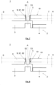
- Fig. 9 shows, as a further exemplary embodiment, the sectional view of a part of a device 1 for measuring current intensities with a resistor arrangement 2 and a printed circuit board 8 positioned on the resistor arrangement 2.
- the contact element 5 has a section 55 with a conical outer contour between the connection element 3 and the printed circuit board 8, which section directly adjoins the printed circuit board 8. Furthermore, the contact element 5 has a projection 56 beyond the printed circuit board 8. In the area of this projection 56, the contact element 5 has been conically widened. As a result, the contact element 5 projects in the lateral direction beyond the upper side 81 of the printed circuit board 8.
- the printed circuit board 8 Due to the conical widening of the contact element 5 in the area of its projection 56, the printed circuit board 8 has been moved in the direction of the connection element 3 and thus onto the conical section 55 of the contact element 5 between the printed circuit board 8 and the connection element 3. In this way, the circuit board 8 is fixed in a force-locking manner in the direction of the longitudinal axis A of the contact element.
- the invention was Figures 1 to 9 explained by way of example using a resistor arrangement 2, which comprises only one resistor element 4 and two terminal connection elements 3, 3'. It is also possible to apply the method described above to resistor arrangements that have two or more resistor elements and at least one further connection element arranged between two resistor elements with respect to a possible current path.
- the resistor arrangement can be configured such that the same current flows through at least two resistor elements, which enables redundant current measurement, or such that different currents flow through at least two resistor elements, which enables the measurement of partial currents.
Landscapes
- Physics & Mathematics (AREA)
- General Physics & Mathematics (AREA)
- Engineering & Computer Science (AREA)
- Microelectronics & Electronic Packaging (AREA)
- Manufacturing & Machinery (AREA)
- Details Of Resistors (AREA)
- Apparatuses And Processes For Manufacturing Resistors (AREA)
Description
- Die Erfindung betrifft ein Verfahren zur Herstellung einer Vorrichtung zur Messung von Stromstärken und eine solche Vorrichtung.
- Für die Strommessung in elektronischen Schaltungen werden Messwiderstände verwendet, die in Reihe zu dem zu überwachenden Bauteil geschaltet sind. Dabei wird die Stromstärke aus der über den als Shunt-Widerstand bezeichneten Messwiderstand abfallenden Spannung bestimmt. Die korrekte und verlässliche Messung der Stromstärke ist beispielsweise besonders wichtig in einem Batteriemanagementsystem eines Elektro- oder Hybridfahrzeugs. Eine Widerstandsanordnung, die einen solchen niederohmigen Messwiderstand mit ungefähr 10 bis 50 µOhm sowie Anschlusselemente zum Verbinden der Widerstandsanordnung mit dem Stromkreis umfasst, kann aus einem längsnahtgeschweißten Verbundmaterial hergestellt werden. Dies ist beispielsweise aus der Druckschrift
EP 0 605 800 A1 bekannt. Das Verbundmaterial wird aus drei Metallbändern hergestellt, indem die einzelnen Metallbänder jeweils über eine Längsnaht miteinander durch ein Elektronenstrahl- oder Laserschweißverfahren verbunden werden. - Die über einem Messwiderstand abfallende Spannung wird über Kontaktstifte oder ähnliche Elemente, die beidseitig vom Messwiderstand auf den Anschlusselementen angeordnet sind, abgegriffen. Solche Kontaktstifte können auf den Anschlusselementen der Widerstandsanordnung aufgelötet, aufgepresst oder aufgeschweißt sein. Die Spannung wird von einer Mess- und Auswerteelektronik erfasst und weiterverarbeitet. Hierfür sind elektronische Bauteile vorgesehen, die auf einer Leiterplatte angeordnet sein können. Die Leiterplatte kann sich dabei in unmittelbarer Nähe der Widerstandsanordnung befinden.
- Aus der Druckschrift
DE 10 2009 031 408 A1 ist eine Widerstandsanordnung mit einem niederohmigen Strommesswiderstand bekannt. Bei dieser Widerstandsanordnung sind zum Abgriff der Spannung Anschlusskontakte vorgesehen, die durch Ausprägung und Gewindeformung in den plattenförmigen Teilstücken, die zum Anschluss der Widerstandsanordnung an den äußeren Stromkreis dienen, gebildet sind. Der Anschluss der Messleitungen zur Spannungsmessung an die Anschlusskontakte erfolgt mittels Kabelschuhen und Befestigungsschrauben. - Des Weiteren ist aus der Druckschrift
US 10 163 553 B2 - Aus der nachveröffentlichten Druckschrift
EP 3 929 594 A1 ist ein Verfahren bekannt, bei dem ein Kontaktstift aus dem Material der Anschlusselemente einer Widerstandsanordnung geformt wird. Der Kontaktstift erstreckt sich durch die Bohrung einer Leiterplatte hindurch und weist einen Überstand über die Leiterplatte auf. Zur Fixierung der Leiterplatte ist der Kontaktstift im Bereich seines Überstands lateral verbreitert. - Die Druckschrift
DE 10 2007 033 182 A1 offenbart ein Widerstandselement mit Anschlussstücken und einem Widerstandsstück, Kontakte werden gebildet werden, indem ein Draht mit gebogenen Enden auf die Anschlussstücke aufgelegt und mit der Oberfläche der Anschlussstücke stoffschlüssig, beispielsweise durch Ultraschallschweißen, verbunden wird. - Die Druckschrift
DE 658 916 offenbart ein Kontaktelement, das aus einem Kontaktstück und einem Nietröhrchen besteht. Das Kontaktstück besteht aus einem flachen, am äußeren Rand durch Stanzen oder Umbiegen abgeschrägten Teil. Das Nietröhrchen wird aus Blech gerollt. - Die Druckschrift
FR 2 544 866 A1 - Die Druckschrift
US 2015/108965 A1 offenbart einen Stromsensor auf Basis eines Shunt-Widerstands. Der Stromsensor umfasst eine Widerstandsanordnung und eine Leiterplatte, auf der sich eine Spanungsmesseinrichtung befindet. Zum Verbinden der Widerstandsanordnung mit der Leiterplatte weist der Stromsensor Abgriffe auf, die seitlich an der Widerstandsanordnung angebracht sind. - Bei den aus dem Stand der Technik bekannten Vorrichtungen ist es notwendig, zusätzliche Bauteile zu verwenden, um die über dem Messwiderstand abfallende Spannung abzugreifen. Dies erfordert zusätzlichen Aufwand und Kosten. Ferner können an den Kontaktstellen der einzelnen Bauteile Kontaktspannungen auftreten, die das Spannungssignal verfälschen können.
- Der Erfindung liegt die Aufgabe zugrunde, ein verbessertes, insbesondere einfacheres und kostengünstigeres Verfahren zur Herstellung einer Vorrichtung zur Messung von Stromstärken und eine solche Vorrichtung anzugeben.
- Die Erfindung wird bezüglich eines Verfahrens durch die Merkmale des Anspruchs 1 und bezüglich einer Vorrichtung durch die Merkmale des Anspruchs 9 wiedergegeben. Die weiteren, rückbezogenen Ansprüche betreffen vorteilhafte Aus- und Weiterbildungen der Erfindung.
- Die Erfindung betrifft ein Verfahren zur Herstellung einer Vorrichtung zur Messung von Stromstärken mittels einer Widerstandsanordnung, wobei das Verfahren folgende Schritte umfasst:
- a) Bereitstellen einer Widerstandsanordnung umfassend mindestens zwei Anschlusselemente, durch welche eine Stromrichtung festgelegt wird, und mindestens ein in Bezug auf die Stromrichtung zwischen den Anschlusselementen angeordnetes Widerstandselement, wobei das mindestens eine Widerstandselement einerseits und die Anschlusselemente andererseits aus unterschiedlichen, elektrisch leitenden Materialien bestehen,
- b) Herausformen mindestens eines Kontaktelements aus dem Material mindestens eines Anschlusselements oder aus dem Material des Widerstandselements, so dass das Kontaktelement monolithisch mit dem Anschlusselement beziehungsweise mit dem Widerstandselement verbunden ist,_wobei das Kontaktelement eine Längsachse aufweist, durch die eine axiale Richtung und eine hierzu senkrechte radiale Richtung definiert werden, und wobei das Kontaktelement so geformt wird, dass es eine von der Widerstandsanordnung abgewandte Stirnseite und einen Hohlraum aufweist, der auf der von der Widerstandsanordnung abgewandten Stirnseite des Kontaktelements offen ist,
- c) Bereitstellen einer Leiterplatte, welche mindestens eine Durchgangsbohrung mit einer inneren Oberfläche aufweist, auf der sich elektrisch leitendes Material befindet,
- d) Positionieren der Leiterplatte auf der Widerstandsanordnung derart, dass die Leiterplatte eine von der Widerstandsanordnung abgewandte Oberseite aufweist und dass das mindestens eine Kontaktelement in die Durchgangsbohrung zumindest hineinragt,
- e) Aufweiten des Kontaktelements in radialer Richtung mittels eines Aufweitmittels, das in axialer Richtung in den Hohlraum des Kontaktelements bis in den Bereich der Durchgangsbohrung der Leiterplatte_eingeführt wird, so dass eine elektrisch leitende Verbindung zwischen dem Kontaktelement und dem elektrisch leitenden Material auf der inneren Oberfläche der Durchgangsbohrung hergestellt wird.
- Unter der Messung von Stromstärken wird auch die Messung der Stärke eines zeitlich sich möglicherweise verändernden elektrischen Stroms verstanden. Die vorstehend beschriebene Widerstandsanordnung kann einen Shunt-Widerstand mit einem Widerstand von 10 bis 50 µOhm als Widerstandselement umfassen. Sowohl das Widerstandselement als auch die Anschlusselemente bestehen aus elektrisch leitenden Materialien. Dabei ist der spezifische elektrische Widerstand des Materials des Widerstandselements deutlich größer, typischerweise mindestens einen Faktor 10 größer als der spezifische elektrische Widerstand des Materials der Anschlusselemente. Andererseits ist der Betrag des Widerstands-Temperaturkoeffizienten des Materials der Anschlusselemente sehr viel größer, typischerweise mindestens einen Faktor 80 größer als der Betrag des Widerstands-Temperaturkoeffizienten des Materials des Widerstandselements. Üblicherweise beträgt der Widerstands-Temperaturkoeffizient des Materials des Widerstandselements weniger als ±5·10-5 1/K, während der Widerstands-Temperaturkoeffizient des Materials der Anschlusselemente ungefähr ±4·10-3 1/K beträgt. Die Anschlusselemente der Widerstandsanordnung können insbesondere aus Kupfer, einer bevorzugt niedriglegierten Kupferlegierung, aus Aluminium oder einer bevorzugt niedriglegierten Aluminiumlegierung bestehen oder mindestens einen dieser Werkstoffe umfassen. Das Widerstandselement kann aus einer Kupferlegierung sein, die als Widerstandslegierung üblicherweise verwendet wird.
- Die Anschlusselemente können endständige Anschlusselemente der Widerstandsanordnung sein. Es ist aber auch möglich, dass mindestens ein Anschlusselement in Bezug auf einen möglichen Strompfad zwischen zwei Widerstandselementen angeordnet ist. Die Widerstandsanordnung kann in planarer Anordnung ausgebildet sein. Dabei sind die Anschlusselemente und das mindestens eine Widerstandselement als platten- oder streifenförmige Elemente gebildet und in einer Ebene nebeneinander, bevorzugt in einer Reihe, angeordnet. Die Dicke des Widerstandselements beziehungsweise der Widerstandselemente kann dabei beliebig sein. Üblicherweise ist sie aber nicht größer als die Dicke der Anschlusselemente.
- Unter Kontaktelement wird ein Werkstoffvorsprung verstanden, der sich über die sonst unverformte Oberfläche eines Anschlusselements oder des Widerstandselements erhebt. Das Formen des Kontaktelements erfolgt durch Verlagern von Material eines Anschlusselements beziehungsweise von Material des Widerstandselements im Wesentlichen in Richtung senkrecht zur Oberfläche des Anschlusselements beziehungsweise des Widerstandselements. Die Richtung, in der das Material verlagert wird, definiert eine axiale Richtung, die parallel zur Längsachse des Kontaktelements ist, und eine hierzu senkrechte, radiale Richtung. Das Kontaktelement wird so geformt, dass es eine von der Widerstandsanordnung abgewandte Stirnseite und einen Hohlraum aufweist, der auf der von der Widerstandsanordnung abgewandten Stirnseite des Kontaktelements offen ist. Das Kontaktelement ist also zumindest teilweise hohl und der Hohlraum erstreckt sich von der Stirnseite des Kontaktelements ausgehend in axialer Richtung in das Kontaktelement hinein. In radialer Richtung wird der Hohlraum durch eine umlaufende, geschlossene Wand aus verlagertem Material eines Anschlusselements beziehungsweise des Widerstandselements begrenzt. Das Kontaktelement weist in diesem Bereich also die Form einer Hülse auf, die zumindest auf einer Seite offen ist. Bevorzugt ist der Hohlraum auf der diametral gegenüberliegenden Seite geschlossen, so dass das Kontaktelement in diesem Bereich eine Form ähnlich einem Becher hat. Die Höhe des Kontaktelements beträgt mindestens 0,5 mm, bevorzugt mindestens 1 mm.
- Die äußere Form des Kontaktelements kann beliebig sein, bevorzugt kreisförmig, rechteckig, quadratisch oder sechseckig. Bevorzugt hat das Kontaktelement im Bereich des Hohlraums einen kreisringförmigen Querschnitt. Form und/oder Größe des Querschnitts des Kontaktelements können konstant sein oder sich entlang der Längsachse des Kontaktelements stetig oder unstetig verändern. Beispielsweise kann das Kontaktelement eine leicht konische Kontur, also eine Kontur mit - bezogen auf die Oberfläche des Anschlusselements beziehungsweise des Widerstandselements - leicht geneigten Begrenzungsflächen aufweisen. Ferner kann das Kontaktelement so geformt werden, dass es einen Absatz aufweist. Unter einem Absatz wird eine unstetige, also sprungartige Veränderung der Querschnittsform und/oder der Querschnittsgröße des Kontaktelements verstanden. Der Absatz kann als Auflage für eine Leiterplatte dienen.
- Das Kontaktelement kann, bevorzugt zusammen mit einem weiteren Kontaktelement, als Spannungsabgriff zur Messung der über dem Widerstandselement abfallenden elektrischen Spannung verwendet werden. Wenn das Kontaktelement aus dem Material des Widerstandselements geformt wird, kann es als Spannungsabgriff zur Messung der über einem Teil des Widerstandselements abfallenden elektrischen Spannung verwendet werden. Alternativ kann das Kontaktelement auch zur Erdung der Widerstandsanordnung dienen. Bevorzugt werden in allen Anschlusselementen der Widerstandsanordnung ein oder mehrere solcher Kontaktelemente geformt. Dabei werden die Kontaktelemente, die zur Spannungsmessung dienen, möglichst nahe an dem Widerstandselement positioniert, an dem der Spannungsabfall ermittelt werden soll.
- Im Rahmen der vorliegenden Erfindung wird unter einer Leiterplatte ein flaches, platten- oder streifenförmiges Bauteil verstanden, das geeignet ist, elektrische Signale in einem elektrisch leitenden Material zu leiten. Ein flaches Bauteil ist platten- oder streifenförmig, wenn zwei gegenüberliegende Flächen des Bauteils zueinander planparallel sind. Der Abstand dieser beiden Flächen definiert die Dicke des Bauteils. Eine Leiterplatte kann beispielsweise ein Metallstreifen sein oder eine Platte aus einem nicht-leitenden Material, auf deren Oberfläche Leiterbahnen aufgebracht sind. Derartige Platten sind unter dem Begriff "printed circuit board" bekannt. Die Leiterplatte weist mindestens eine Durchgangsbohrung mit einer inneren Oberfläche auf, auf der sich elektrisch leitendes Material befindet. Dies schließt auch den Fall ein, dass die Leiterplatte ein Metallstreifen oder ein Metallplättchen ist, so dass sich auf der inneren Oberfläche der Durchgangsbohrung in inhärenter Weise elektrisch leitendes Material befindet. Falls die Leiterplatte eine Platte aus nicht-leitendem Material ist, auf deren Oberfläche Leiterbahnen aufgebracht sind, kann das elektrisch leitende Material auf der inneren Oberfläche der Durchgangsbohrung mit einer Leiterbahn verbunden sein, die bevorzugt auf der von der Widerstandsanordnung abgewandten Seite der Leiterplatte angeordnet ist. Ferner können auf einer solchen Leiterplatte elektrische Bauteile angeordnet sein, die zur Messung und Auswertung von elektrischen Signalen dienen. Mit dem Begriff Durchgangsbohrung wird eine Aussparung in der Leiterplatte bezeichnet, die sich über die gesamte Dicke der Leiterplatte erstreckt. Die Durchgangsbohrung kann eine zylindrische Form haben. Alternativ ist auch eine konische Form möglich.
- Die Leiterplatte wird auf der Widerstandsanordnung in einer Weise positioniert, dass das mindestens eine Kontaktelement in die Durchgangsbohrung zumindest hineinragt. Die Leiterplatte wird dabei im Wesentlichen planparallel zur Widerstandsanordnung positioniert, so dass die Leiterplatte eine von der Widerstandsanordnung abgewandte Oberseite und eine der Widerstandsanordnung zugewandte Unterseite aufweist. Zwischen der Leiterplatte und der Widerstandsanordnung kann ein Abstand sein. Es ist jedoch auch möglich, dass die Leiterplatte direkt auf der Widerstandsanordnung aufliegt. Das Kontaktelement sollte mindestens bis zur Hälfte der Dicke der Leiterplatte, bevorzugt mindestens bis zu 70 % der Dicke der Leiterplatte, in die Durchgangsbohrung der Leiterplatte hineinragen.
- Anschließend wird das Kontaktelement in radialer Richtung mittels eines geeigneten Aufweitmittels aufgeweitet. Hierzu wird das Aufweitmittel ausgehend von der Oberseite der Leiterplatte in axialer Richtung in den Hohlraum des Kontaktelements eingeführt. Das Aufweitmittel ist so ausgebildet, dass es das Kontaktelement im Bereich des Hohlraums in radialer Richtung aufweiten kann. Hierzu wird das Material des Kontaktelements, das den Hohlraum in radialer Richtung begrenzt, in radialer Richtung soweit nach Außen verlagert, dass es mit der inneren Oberfläche der Durchgangsbohrung der Leiterplatte in Kontakt kommt. Auf diese Weise wird eine elektrisch leitende Verbindung zwischen dem Kontaktelement und dem elektrisch leitenden Material auf der inneren Oberfläche der Durchgangsbohrung hergestellt. Die durch das Aufweiten bewirkte Vergrößerung der Außenabmessung des Kontaktelements beträgt bevorzugt zwischen 2 % und 15 % seiner Außenabmessung vor dem Aufweiten. Durch das Aufweiten wird ferner die Wanddicke des Kontaktelements reduziert. Eine Reduktion um mindestens 20 % der ursprünglichen Wanddicke ist günstig. Das Aufweitmittel kann ein geeignetes Werkzeug sein, das nach dem Aufweiten wieder aus dem Hohlraum des Kontaktelements entfernt wird.
- Der Vorteil des beschriebenen Verfahrens besteht darin, dass zur Herstellung der Verbindung zwischen Widerstandsanordnung und Leiterplatte keine zusätzlichen Bauteile und/oder Materialien benötigt werden. Weil das Kontaktelement direkt aus dem Material eines Anschlusselements oder des Widerstandselements geformt wird, ist es nicht erforderlich, das Kontaktelement separat auf der Widerstandsanordnung oder auf der Leiterplatte zu montieren. Es entfallen die hierfür notwendigen Arbeitsschritte und die benötigten Materialien, wie beispielsweise Lot. Mehrere Kontaktelemente können gleichzeitig geformt werden.
- Durch die monolithische Verbindung zwischen Kontaktelement und Anschlusselement beziehungsweise zwischen Kontaktelement und Widerstandselement werden unerwünschte Kontaktspannungen, die eine Messung verfälschen können, vermieden.
- Ein besonders vorteilhafter Aspekt des vorgeschlagenen Verfahrens ist das radiale Aufweiten des Kontaktelements durch ein geeignetes Aufweitmittel. Weil das Aufweitmittel in den Hohlraum des Kontaktelements eingeführt wird, erfolgt die Verbindung zwischen Kontaktelement und Leiterplatte im Wesentlichen im Bereich der Durchgangsbohrung. Somit ist es nicht erforderlich, dass das Kontaktelement über die Leiterplatte hinausragt, also einen Überstand über die Oberseite der Leiterplatte aufweist. Zur Formung des Kontaktelements muss das Material des Anschlusselements oder des Widerstandselements somit nur in einem geringen Maß verformt werden. Die notwendigen Kräfte sind gering. Dies ist vorteilhaft hinsichtlich der Werkzeugstandzeit und der Prozessgeschwindigkeit. Besonders vorteilhaft anwendbar ist das vorgeschlagene Verfahren, wenn ein oder mehrere Kontaktelemente aus dem Widerstandselement geformt werden sollen. Das Material des Widerstandselements ist üblicherweise schwerer unformbar als das Material der Anschlusselemente. Je weniger weit es verformt werden muss, desto einfacher ist der Prozess.
- Das Aufweitmittel kann auch ein Körper sein, der dauerhaft im Hohlraum des Kontaktelements verbleibt. Ein solcher Körper kann beispielsweise ein Stopfen oder ein Niet sein. Durch einen solchen Körper wird ein besonders verlässlicher und dauerhafter Kontakt zwischen dem Kontaktelement und der inneren Oberfläche der Durchgangsbohrung der Leiterplatte hergestellt.
- Wird die Widerstandsanordnung hergestellt, indem sie aus einem längsnahtgeschweißten, bandförmigen Verbundmaterial abgelängt wird, dann können die Kontaktelemente bevorzugt gleichzeitig mit dem Ablängen des Verbundmaterials geformt werden. Die Schritte a) und b) des Verfahrens erfolgen in diesem Fall also gleichzeitig. Ein separater, zusätzlicher Arbeitsschritt für das Formen der Kontaktelemente ist somit nicht notwendig. Das Verfahren ist somit schneller und kostengünstiger, als wenn die Kontaktelemente erst nach dem Ablängen des Verbundmaterials geformt werden. Ferner wird auf diese Weise eine hohe Positionsgenauigkeit der Kontaktelemente erreicht.
- Im Rahmen einer Ausführungsform der Erfindung kann das Aufweitmittel so gestaltet sein, dass das Aufweiten des Kontaktelements durch das Einführen des Aufweitmittels erfolgt. Das Kontaktelement wird also bereits während des Einführens des Aufweitmittels in den Hohlraum in radialer Richtung aufgeweitet. Hierzu weist das Aufweitmittel zumindest teilweise eine konische Außenkontur auf. Diese Außenkontur führt zu einer radialen Verlagerung des Materials des Kontaktelements, wenn das Aufweitmittel in den Hohlraum eingeführt wird. Damit werden kurze Bearbeitungszeiten ermöglicht.
- Im Rahmen einer hierzu alternativen Ausführungsform der Erfindung kann das Aufweitmittel so gestaltet sein, dass das Aufweiten des Kontaktelements nach dem Einführen des Aufweitmittels erfolgt. Das Kontaktelement wird also im Wesentlichen erst nach dem Einführen des Aufweitmittels in den Hohlraum in radialer Richtung aufgeweitet. Hierzu weist das Aufweitmittel einen Abschnitt auf, dessen Außendurchmesser kleiner als der Innendurchmesser des Hohlraums ist. Das Einführen dieses Abschnitts des Aufweitmittels in den Hohlraum erfolgt dann ohne signifikanten Widerstand und somit auch ohne ungewollte Verformung des Kontaktelements. Nach dem Einführen des Aufweitmittels erfolgt das radiale Aufweiten des Kontaktelements mittels eines geeigneten Mechanismus. Falls das Aufweitmittel ein Werkzeug ist, kann dies beispielsweise durch ein Spreizen des Werkzeugs, durch eine exzentrische Rotation des Werkzeugs oder durch elektromagnetische Kräfte erfolgen
- Im Rahmen einer bevorzugten Ausführungsform der Erfindung kann durch das Aufweiten in Verfahrensschritt e) auch gleichzeitig eine kraftschlüssige Verbindung zwischen der inneren Oberfläche der Durchgangsbohrung der Leiterplatte und dem Kontaktelement hergestellt werden. Hierzu erfolgt das Aufweiten des Kontaktelements in einem Ausmaß, dass das Material an die innere Oberfläche der Durchgangsbohrung der Leiterplatte so stark angedrückt wird, dass eine Presspassung ausgebildet wird. Die Wanddicke des Kontaktelements wird dabei bevorzugt um mindestens 40 % reduziert. Durch die Ausbildung der Presspassung können andere Mittel zur mechanischen Fixierung der Leiterplatte auf der Widerstandsanordnung eingespart werden.
- Im Rahmen einer speziellen Ausgestaltung dieser Ausführungsform der Erfindung kann durch das Aufweiten in Verfahrensschritt e) auch gleichzeitig eine formschlüssige Verbindung zwischen der inneren Oberfläche der Durchgangsbohrung der Leiterplatte und dem Kontaktelement hergestellt werden. Beispielsweise kann die Durchgangsbohrung der Leiterplatte eine konische Form haben und so gestaltet sein, dass sich der Innendurchmesser von der Unterseite der Leiterplatte zu deren Oberseite hin vergrößert. Bei Verwendung eines Aufweitmittels mit angepasster konischer Außenkontur führt das Aufweiten des Kontaktelements zu einer formschlüssigen Verbindung. Eine solche Verbindung stellt eine besonders sichere Art der Verbindung dar.
- Im Rahmen einer bevorzugten Ausführungsform der Erfindung kann das Kontaktelement eine Höhe aufweisen, die so gewählt ist, dass nach dem Positionieren der Leiterplatte die von der Widerstandsanordnung abgewandte Stirnseite des Kontaktelements sich innerhalb der Durchgangsbohrung der Leiterplatte befindet oder mit der Oberseite der Leiterplatte bündig abschließt. Die Höhe bezeichnet dabei die Erstreckung des Kontaktelements in axialer Richtung gemessen ab der unverformten Oberfläche des Anschlusselements beziehungsweise des Widerstandselements. Die Höhe ist also so bemessen, dass die Eindringtiefe des Kontaktelements in die Durchgangsbohrung der Leiterplatte maximal gleich der Dicke der Leiterplatte ist. Mit anderen Worten, das Kontaktelement weist bei dieser Ausführungsform keinen Überstand über die Oberseite der Leiterplatte auf. Ein Kontaktelement von so geringer Höhe lässt sich besonders günstig formen. Im Rahmen einer speziellen Ausgestaltung dieser Ausführungsform der Erfindung kann die Eindringtiefe des Kontaktelements in die Durchgangsbohrung der Leiterplatte 80 bis 100 % der Dicke der Leiterplatte betragen. Dies stellt ein Optimum zwischen dem notwendigen Aufwand bei der Formung des Kontaktelements und der Qualität des Kontakts zwischen Kontaktelement und Leiterplatte dar.
- Im Rahmen einer weiteren Ausführungsform der Erfindung kann das Formen des Kontaktelements in Verfahrensschritt b) durch einen Prägeschritt oder durch Fließpressen erfolgen. Prägen und Fließpressen eignen sich besonders zur Formung von monolithisch mit dem Material der Anschlusselemente oder des Widerstandselements verbundenen Kontaktelementen, die sich im Wesentlichen senkrecht zur Oberfläche der Anschlusselemente beziehungsweise des Widerstandselements erstrecken. Das Formen des Materials erfolgt dabei mittels eines Stempels und einer geeigneten Negativform.
- Im Rahmen einer speziellen Ausgestaltung dieser Ausführungsform der Erfindung kann zur Formgebung des Kontaktelements eine Negativform mit mindestens einer der äußeren Kontur des Kontaktelements entsprechenden Aussparung und mindestens einem in der Aussparung positionierten Innenwerkzeug zur Formung des Hohlraums verwendet werden, wobei während Verfahrensschritt b) das Innenwerkzeug in Richtung der Längsachse des Kontaktelements relativ zur Aussparung bewegt wird. Dies hat sich als umformtechnisch besonders günstige Prozessführung erwiesen, so dass Kontaktelemente mit einer großen Höhe erzeugt werden können.
- Im Rahmen einer weiteren speziellen Ausgestaltung der Erfindung kann das Aufweiten des Kontaktelements in Verfahrensschritt e) durch Erwärmen des Materials des Kontaktelements mittels Ultraschall oder mittels eines Lasers unterstützt werden. Das Material des Kontaktelements ist aufgrund der Verformung in Verfahrensschritt b) verfestigt und hart. Dies ist für die nachfolgende Verformung in Schritt e) hinderlich. Durch den Eintrag von Wärme mittels eines Lasers oder mittels Ultraschall kann das Material des Kontaktelements soweit erwärmt werden, dass es sich zumindest teilweise entfestigt, also weicher wird. Das Verformen in Schritt e) ist dann leichter möglich.
- Hinsichtlich weiterer technischer Merkmale und Vorteile des erfindungsgemäßen Verfahrens wird hiermit explizit auf die nachstehenden Erläuterungen im Zusammenhang mit einer Vorrichtung zur Messung von Stromstärken sowie auf die Figuren und die Figurenbeschreibung verwiesen.
- Ein weiterer Aspekt der Erfindung betrifft eine Vorrichtung zur Messung von Stromstärken. Hierunter wird auch die Messung der Stärke eines zeitlich sich möglicherweise verändernden elektrischen Stroms verstanden. Die Vorrichtung umfasst eine Widerstandsanordnung und eine mit der Widerstandsanordnung mechanisch und elektrisch verbundene Leiterplatte. Die Widerstandsanordnung umfasst mindestens zwei Anschlusselemente, die eine Stromrichtung definieren, und mindestens ein in Bezug auf die Stromrichtung zwischen den Anschlusselementen angeordnetes Widerstandselement, wobei das mindestens eine Widerstandselement einerseits und die Anschlusselemente andererseits aus unterschiedlichen, elektrisch leitenden Materialien bestehen. Die Leiterplatte weist mindestens eine Durchgangsbohrung mit einer inneren Oberfläche auf, auf der sich elektrisch leitendes Material befindet. Die Widerstandsanordnung weist mindestens ein Kontaktelement mit einer Längsachse auf, das monolithisch mit einem der Anschlusselemente verbunden und aus dem Material des Anschlusselements herausgearbeitet ist, oder das monolithisch mit dem Widerstandselement verbunden und aus dem Material des Widerstandselements herausgearbeitet ist. Durch dieses Kontaktelement ist die Widerstandsanordnung mit der Leiterplatte elektrisch leitend und mechanisch verbunden, indem das Kontaktelement in die Durchgangsbohrung der Leiterplatte zumindest hineinragt und mit dem elektrisch leitenden Material auf der inneren Oberfläche der Durchgangsbohrung kraftschlüssig verbunden ist. Hierzu weist das Kontaktelement eine von der Widerstandsanordnung abgewandten Stirnseite und einen Hohlraum auf, der auf der von der Widerstandsanordnung abgewandten Stirnseite des Kontaktelements offen ist. Am Übergang von seiner Stirnseite zum Hohlraum weist das Kontaktelement auf seiner Innenseite eine konische Kontur auf, die sich bis in den Bereich der Durchgangsbohrung der Leiterplatte erstreckt.
- Hinsichtlich der zur Beschreibung der Vorrichtung verwendeten Begriffe wird hiermit explizit auf die vorstehenden Erläuterungen der Begriffe im Zusammenhang mit der Beschreibung des Verfahrens zur Herstellung einer Vorrichtung zur Messung von Stromstärken verwiesen.
- Der besondere Vorteil der beschriebenen Vorrichtung besteht darin, dass durch die monolithische Verbindung zwischen Kontaktelement und Anschlusselement beziehungsweise Widerstandselement unerwünschte Kontaktspannungen, die eine Messung verfälschen können, vermieden werden. Ferner kann die Vorrichtung kostengünstig und mit hoher Präzision hergestellt werden, denn das Kontaktelement ist unmittelbar aus dem Material des Anschlusselements oder des Widerstandselements herausgeformt. Ein besonders vorteilhafter Aspekt der beschriebenen Vorrichtung ist die kraftschlüssige Verbindung zwischen der Leiterplatte und der Widerstandsanordnung. Diese Verbindung wird durch das Kontaktelement hergestellt, welches durch einen Aufweitprozess mit der inneren Oberfläche der Durchgangsbohrung der Leiterplatte in elektrischen und mechanischen Kontakt gebracht wird. Zur Durchführung dieses Aufweitprozesses weist das Kontaktelement eine von der Widerstandsanordnung abgewandte Stirnseite und einen Hohlraum auf, der auf der von der Widerstandsanordnung abgewandten Stirnseite des Kontaktelements offen ist. Am Übergang von seiner Stirnseite zum Hohlraum weist das Kontaktelement auf seiner Innenseite_eine konische Kontur auf. Diese konische Kontur ist das Resultat des Aufweitprozesses und sie kann zur leichteren Einführung eines Aufweitmittels in den Hohlraum des Kontaktelements dienen.
- Im Rahmen einer Ausführungsform der Erfindung kann das Kontaktelement eine Höhe aufweisen, die so gewählt ist, dass die von der Widerstandsanordnung abgewandte Stirnseite des Kontaktelements sich innerhalb der Durchgangsbohrung der Leiterplatte befindet oder mit der Oberseite der Leiterplatte bündig abschließt. Die Höhe bezeichnet dabei die Erstreckung des Kontaktelements in Richtung seiner Längsachse gemessen ab der unverformten Oberfläche des Anschlusselements beziehungsweise des Widerstandselements. Die Höhe ist also so bemessen, dass die Eindringtiefe des Kontaktelements in die Durchgangsbohrung der Leiterplatte maximal gleich der Dicke der Leiterplatte ist. Mit anderen Worten, das Kontaktelement weist keinen Überstand über die Oberseite der Leiterplatte auf. Ein Kontaktelement mit dieser geringen Höhe lässt sich besonders günstig formen. Im Rahmen einer speziellen Ausgestaltung dieser Ausführungsform der Erfindung kann die Eindringtiefe des Kontaktelements in die Durchgangsbohrung der Leiterplatte 80 bis 100 % der Dicke der Leiterplatte betragen. Dies stellt ein Optimum zwischen dem notwendigen Aufwand bei der Formung des Kontaktelements und der Qualität des Kontakts zwischen Kontaktelement und Leiterplatte dar.
- Im Rahmen einer alternativen Ausführungsform der Erfindung kann das Kontaktelement auf der von der Widerstandsanordnung abgewandten Seite der Leiterplatte einen Überstand über die Leiterplatte aufweisen und zur Fixierung der Leiterplatte im Bereich dieses Überstands lateral verbreitert sein, bevorzugt konisch aufgeweitet sein. Durch das laterale Verbreitern, insbesondere durch konisches Aufweiten des Kontaktelements im Bereich dieses Überstands über die Leiterplatte wird die Leiterplatte in axialer Richtung des Kontaktelements, also in Richtung zum Anschlusselement der Widerstandsanordnung hin, zumindest in einer Richtung formschlüssig fixiert. Das laterale Verbreitern kann außer durch konisches Aufweiten auch durch andere Verformungen des Kontaktelements erfolgen. Beispiele hierfür sind Crimpen, Bördeln, partielles Umbiegen und Aufweiten mittels eines kugelförmigen, zylindrischen oder balligen Werkzeugs.
- Im Rahmen einer besonderen Ausgestaltung dieser alternativen Ausführungsform der Erfindung kann das Kontaktelement zwischen dem Anschlusselement und der Leiterplatte einen Abschnitt mit einer konischen Außenkontur aufweisen. Der konische Abschnitt ist dabei so gewählt, dass sich die Querschnittsfläche des Kontaktelements zum Anschlusselement hin vergrößert. Der Abschnitt mit der konischen Kontur schließt unmittelbar an die Leiterplatte an. Durch die konische Außenkontur vergrößert sich die Querschnittsfläche des Kontaktelements stetig und mindestens so weit, dass diese größer als die Querschnittsfläche der Durchgangsbohrung der Leiterplatte ist. Zusammen mit dem konischen Aufweiten des Kontaktelements im Bereich seines Überstands kann somit eine form- und kraftschlüssige Fixierung der Leiterplatte sowohl in Richtung der Achse des Kontaktelements als auch senkrecht hierzu erreicht werden. Die Leiterplatte ist durch das Kontaktelement doppelt-konisch verklemmt. Diese Ausgestaltung der Erfindung ist besonders resistent gegen mechanische Belastungen wie beispielsweise Vibrationen.
- Im Rahmen einer weiteren vorteilhaften Ausführungsform der Vorrichtung kann das mindestens eine Kontaktelement einen Absatz aufweisen, auf dem die Leiterplatte in einer Weise aufliegt, dass die Leiterplatte vom Anschlusselement und somit von der Widerstandsanordnung beabstandet ist. Der Abstand zwischen der Leiterplatte und der Widerstandsanordnung bewirkt eine bessere thermische Entkopplung der Leiterplatte von der Widerstandsanordnung. Die Wärme, die bei Stromfluss durch das Widerstandselement entsteht, kann in diesem Fall nicht direkt vom Widerstandselement oder von einem Anschlusselement auf die Leiterplatte übertragen werden, sondern die Wärme muss durch das Kontaktelement strömen. Aufgrund seines relativ kleinen Querschnitts stellt das Kontaktelement einen großen Wärmewiderstand dar. Der Wärmestrom von der Widerstandsanordnung zur Leiterplatte wird deshalb reduziert und die Leiterplatte bleibt auf einem niedrigeren Temperaturniveau, als wenn die Leiterplatte direkt auf einem Anschlusselement aufliegen würde. Diese Ausführungsform ist besonders dann vorteilhaft, wenn die Dicke des Widerstandselements nicht kleiner als die jeweilige Dicke der Anschlusselemente ist.
- Ferner kann im Rahmen einer besonders vorteilhaften Ausführungsform der Vorrichtung vorgesehen sein, dass ein erstes Kontaktelement zwischen dem Anschlusselement und der Leiterplatte einen konischen Abschnitt aufweist, während ein zweites Kontaktelement zwischen dem Anschlusselement und der Leiterplatte einen Absatz aufweist, auf dem die Leiterplatte aufliegt. Insbesondere können beide Kontaktelemente hierbei auf der von der Widerstandsanordnung abgewandten Seite der Leiterplatte jeweils einen Überstand über die Leiterplatte aufweisen und im Bereich des Überstands lateral verbreitert sein. Der besondere Vorteil einer solchen Kombination von Kontaktelementen mit unterschiedlicher Form und Funktion ist, dass bei der überlagerten Belastung aus Vibration und Temperaturwechsel das erste Kontaktelement für eine Fixierung der Leiterplatte in lateraler Richtung sorgt, während das zweite Kontaktelement eine Fixierung der Leiterplatte in Richtung senkrecht zur Leiterplatte ermöglicht, ohne dabei eine zusätzliche Einschränkung der Bewegungsfreiheit in lateraler Richtung zu bewirken. Spannungen, die bei Änderung der Temperatur aufgrund unterschiedlicher Ausdehnung von Leiterplatte und Widerstandsanordnung entstehen können, werden somit reduziert. Die Vorrichtung ist somit besonders robust.
- In vorteilhafter Ausgestaltung der Erfindung kann die Oberfläche des mindestens einen Kontaktelements eine metallische Beschichtung, insbesondere eine zinn-, silber- oder nickelhaltige Beschichtung, aufweisen. Eine solche Beschichtung verhindert Korrosion und kann somit dafür sorgen, dass der elektrische Kontakt zwischen dem Kontaktelement und dem elektrisch leitenden Material auf der inneren Oberfläche der Durchgangsbohrung über die gesamte Lebensdauer der Vorrichtung von hoher Güte ist. Die Beschichtung kann dabei vor dem Formen des Kontaktelements in Schritt b) aufgebracht worden sein oder das Kontaktelement kann in einem separaten Schritt zwischen den Verfahrensschritten b) und c) beschichtet worden sein.
- Hinsichtlich weiterer technischer Merkmale und Vorteile der erfindungsgemäßen Vorrichtung wird hiermit explizit auf die Erläuterungen im Zusammenhang mit dem vorstehend beschriebenen erfindungsgemäßen Verfahren sowie auf die Figuren und die Figurenbeschreibung verwiesen.
- Ausführungsbeispiele der Erfindung werden anhand der schematischen Zeichnungen näher erläutert.
- Darin zeigen:
-
Fig. 1 eine Schrägansicht einer Widerstandsanordnung -
Fig. 2 eine Seitenansicht einer Widerstandsanordnung -
Fig. 3 in Schnittansicht einen Ausschnitt aus einer Widerstandsanordnung bei Abschluss von Verfahrensschritt b) -
Fig. 4 in Schnittansicht einen Ausschnitt aus einer Widerstandsanordnung mit geformtem Kontaktelement -
Fig. 5 in Schnittansicht einen Ausschnitt aus einer Widerstandsanordnung mit darauf positionierter Leiterplatte -
Fig. 6 in Schnittansicht einen Ausschnitt aus einer Widerstandsanordnung während Verfahrensschritt e) -
Fig. 7 in Schnittansicht einen Ausschnitt aus einer Widerstandsanordnung mit darauf fixierter Leiterplatte -
Fig. 8 in Schnittansicht einen Ausschnitt aus einer Widerstandsanordnung mit darauf fixierter Leiterplatte und mit Kontaktelement mit Absatz -
Fig. 9 in Schnittansicht einen Ausschnitt aus einer Widerstandsanordnung mit darauf fixierter Leiterplatte und mit Kontaktelement mit konischem Abschnitt - Einander entsprechende Teile sind in allen Figuren mit denselben Bezugszeichen versehen.
-
Fig. 1 zeigt eine Schrägansicht einer Widerstandsanordnung 2 noch ohne ein Kontaktelement. Die Widerstandsanordnung 2 weist zwei endständige Anschlusselemente 3, 3' und ein Widerstandselement 4 auf, welches zwischen den beiden Anschlusselementen 3, 3' positioniert ist. Die Anschlusselemente 3, 3' und das Widerstandselement 4 haben jeweils eine plattenförmige Form. Die Dicke des Widerstandselements 4 ist etwas geringer als die jeweilige Dicke der beiden Anschlusselemente 3, 3'. Die Widerstandsanordnung 2 kann an den beiden Anschlusselementen 3, 3' mit einem Stromkreis verbunden werden. Zu diesem Zweck können die beiden Anschlusselemente 3, 3' nicht dargestellte Verbindungsvorrichtungen aufweisen, beispielsweise Bohrungen. Diese Verbindungsvorrichtungen sind jeweils in dem Bereich der Anschlusselemente 3, 3' angebracht, der vom Widerstandselement 4 entfernt ist. Das Widerstandselement 4 befindet sich bezogen auf die Richtung des Stromflusses zwischen den Anschlusselementen 3, 3'. Bei Stromfluss fällt über dem Widerstandselement 4 eine elektrische Spannung ab, anhand derer die Stärke des durch die Widerstandsanordnung 2 fließenden Stroms ermittelt werden kann. -
Fig. 2 zeigt eine Seitenansicht der Widerstandsanordnung 2 gemäßFig. 1 . Eine Widerstandsanordnung 2 wie inFiguren 1 und 2 dargestellt kann in bekannter Weise durch Längsnahtschweißen von drei Bändern zu einem Verbundmaterial und anschließendes Ablängen des geschweißten Verbundmaterials hergestellt werden. -
Fig. 3 zeigt in Schnittansicht einen vergrößerten Ausschnitt der Widerstandsanordnung 2 gemäßFig. 1 und 2 bei Abschluss von Verfahrensschritt b). Auf der Oberseite des Anschlusselements 3 wurde eine Negativform 12 mit einer Aussparung 121 und einem in der Aussparung 121 angeordneten Innenwerkzeug 122 positioniert. Auf der Unterseite des Anschlusselements 3 ist ein Stempel 11 in das Material des Anschlusselements 3 eingedrungen, was durch den nach oben gerichteten Pfeil symbolisiert ist. Der Stempel 11 ist so positioniert, dass er der Aussparung 121 der Negativform 12 gegenüberliegt. Durch das Eindringen des Stempels 11 wurde Material des Anschlusselements 3 im Wesentlichen senkrecht zur Oberfläche des Anschlusselements 3 verformt und in den leeren Raum der Negativform 12 verlagert, welcher durch die Aussparung 121 und das Innenwerkzeug 122 definiert ist. Auf diese Weise wurde ein Werkstoffvorsprung geformt, der das Kontaktelement 5 bildet. Das Innenwerkzeug 122 bewirkt, dass das Kontaktelement 5 nach Entfernung des Innenwerkzeugs 122 einen einseitig offenen Hohlraum aufweist. -
Fig. 4 zeigt in Schnittansicht einen vergrößerten Ausschnitt der Widerstandsanordnung 2 mit einem geformten Kontaktelement 5 nach Verfahrensschritt b). Der Stempel 11 und die Negativform 12 wurden entfernt. Um das Entfernen von Stempel 11 und Negativform 12 zu erleichtern, können der Stempel 11, die Aussparung 121 und das Innenwerkzeug 122 in der Negativform 12 jeweils eine Kontur mit Schrägen zur Entformung aufweisen. Dementsprechend können die geformten Kontaktelemente 5 ebenfalls eine Kontur mit Schrägen aufweisen. Der Winkel, den die Schrägen zur Entformung mit der Normalen auf die Oberfläche der Anschlusselemente 3 einschließen, beträgt typischerweise ungefähr 2°. Aufgrund dieser geringen Abweichung von der Normalen sind die Schrägen in den Figuren nicht explizit dargestellt. - Das Kontaktelement 5 weist eine Längsachse A auf, die senkrecht zur Oberfläche des Anschlusselements 3 orientiert ist. Ferner weist das Kontaktelement 5 eine Stirnseite 52 auf, die vom Anschlusselement 3 und somit von der Widerstandsanordnung 2 abgewandt ist. Ausgehend von dieser Stirnseite 52 erstreckt sich ein Hohlraum 53 entlang der Längsachse A des Kontaktelements 5. Im dargestellten Fall erstreckt sich dieser Hohlraum 53 ungefähr bis zur unverformten Oberfläche des Anschlusselements 3. Aus fertigungstechnischen Gründen kann es jedoch vorteilhaft sein, das Kontaktelement 5 so zu formen, dass sich der Hohlraum 53 weniger weit in das Kontaktelement 5 erstreckt oder alternativ, dass der Hohlraum 53 bis in das Material des Anschlusselements 3 hinein reicht. Durch den Hohlraum 53 hat das Kontaktelement 5 die Form einer Hülse, die auf einer Seite geschlossen und auf der anderen Seite offen ist. Die Höhe des Kontaktelements 5 ist mit dem Symbol H gekennzeichnet. Die Höhe H wird ausgehend von der unverformten Oberfläche des Anschlusselements 3 bis zur Stirnseite 52 des Kontaktelements 5 gemessen.
- Das Kontaktelement 5 ist zum Abgreifen der über dem Widerstandselement 4 abfallenden elektrischen Spannung vorgesehen. Um Verfälschungen des Messwerts zu minimieren, wurde das Kontaktelement 5 so aus dem Anschlusselement 3 geformt, dass es nahe an der Verbindungsstelle zwischen dem Anschlusselement 3 und dem Widerstandselement 4 positioniert ist.
-
Fig. 5 zeigt in Schnittansicht den vergrößerten Ausschnitt der Widerstandsanordnung 2 gemäßFig. 4 zusätzlich mit einer auf der Widerstandsanordnung 2 positionierten Leiterplatte 8 der Dicke D.Fig. 5 stellt somit die Widerstandsanordnung 2 und die Leiterplatte 8 nach Verfahrensschritt d) dar. Die Leiterplatte 8 weist eine Durchgangsbohrung 9 auf. Auf der inneren Oberfläche 91 der Durchgangsbohrung 9 der Leiterplatte 8 befindet sich elektrisch leitendes Material 92, das aus Gründen der Übersichtlichkeit nicht näher dargestellt ist. Die Leiterplatte 8 wurde so positioniert, dass das Kontaktelement 5 in die Durchgangsbohrung 9 bis zu einer Eindringtiefe T hineinragt. Im dargestellten Fall ist die Eindringtiefe T etwas geringer als die Dicke D der Leiterplatte 8, so dass die Stirnseite 52 des Kontaktelements 5 nicht bündig mit der Oberseite 81 der Leiterplatte 8 abschließt, sondern sich noch innerhalb der Durchgangsbohrung 9 befindet. Die Eindringtiefe T beträgt ungefähr 90 % der Dicke D der Leiterplatte 8. Die lichte Weite der Durchgangsbohrung 9 ist geringfügig größer als die äußere Abmessung des Kontaktelements 5. Im dargestellten Ausführungsbeispiel liegt die Leiterplatte 8 nicht unmittelbar auf dem Anschlusselement 3 auf, was beispielsweise durch nicht dargestellte Abstandshalter erreicht werden kann. Ein großer Abstand zwischen der Leiterplatte 8 und dem Widerstandselement 4 ist vorteilhaft, weil dadurch Wärme, die im Widerstandselement entsteht, schnell abgeführt werden kann. Auf der Leiterplatte 8 möglicherweise vorhandene, elektronische Bauteile sind aus Gründen der Übersichtlichkeit nicht dargestellt. -
Fig. 6 zeigt in Schnittansicht den vergrößerten Ausschnitt der Widerstandsanordnung 2 während Verfahrensschritt e). Ein Aufweitmittel 14 mit konischer Form wird in Pfeilrichtung in den Hohlraum 53 des Kontaktelements 5 eingeführt. Die äußere Abmessung des Aufweitmittels 14 ist so gewählt, dass durch die konische Form des Aufweitmittels 14 das Material des Kontaktelements 5 in radialer Richtung nach außen, also zur inneren Oberfläche 91 der Durchgangsbohrung 9 hin, verlagert wird. Hierdurch kommt das Kontaktelement 5 unter Bildung einer elektrisch leitenden Verbindung mit dem elektrisch leitenden Material 92 auf der inneren Oberfläche 91 der Durchgangsbohrung 9 in Kontakt. Das inFig. 6 dargestellte Aufweitmittel 14 kann ein Körper sein, der im Hohlraum 53 des Kontaktelements 5 verbleibt, oder es kann der Arbeitsbereich eines Werkzeugs sein, das nach dem Aufweiten wieder aus dem Hohlraum 53 des Kontaktelements 5 entfernt wird. -
Fig. 7 zeigt in Schnittansicht den vergrößerten Ausschnitt der Widerstandsanordnung 2 gemäßFig. 6 nach Entfernen des zum Aufweiten verwendeten Werkzeugs.Fig. 7 stellt somit gleichzeitig die Schnittansicht eines Teils einer Vorrichtung 1 zur Messung von Stromstärken mittels der Widerstandsanordnung 2 dar. -
Fig. 8 zeigt als weiteres Ausführungsbeispiel die Schnittansicht eines Teils einer Vorrichtung 1 zur Messung von Stromstärken mit einer Widerstandsanordnung 2 und einer auf der Widerstandsanordnung 2 positionierten Leiterplatte 8. Das Kontaktelement 5 weist einen umlaufenden Absatz 51 auf, auf dem die Leiterplatte 8 aufliegt. Zu diesem Zweck ist das Kontaktelement 5 so gestaltet, dass die äußere Abmessung des Kontaktelements 5 in dem Teilbereich, der unmittelbar an das Anschlusselement 3 angrenzt, größer als die lichte Weite der Durchgangsbohrung 9 der Leiterplatte 8 ist. Somit liegt die Leiterplatte 8 auch ohne zusätzliche Abstandshalter weder auf dem Anschlusselement 3 noch auf dem Widerstandselement 4 auf. Bei der Formung des Kontaktelements 5 aus dem Material des Anschlusselements 3 wurde die Höhe des Absatzes 51 bereits berücksichtigt. Die Kontaktierung der Leiterplatte 8 durch das Kontaktelement 5 erfolgt in gleicher Weise wie bei dem inFig. 6 dargestellten und im Zusammenhang mitFig. 6 erläuterten Ausführungsbeispiel. -
Fig. 9 zeigt als weiteres Ausführungsbeispiel die Schnittansicht eines Teils einer Vorrichtung 1 zur Messung von Stromstärken mit einer Widerstandsanordnung 2 und einer auf der Widerstandsanordnung 2 positionierten Leiterplatte 8. Das Kontaktelement 5 weist zwischen dem Anschlusselement 3 und der Leiterplatte 8 einen Abschnitt 55 mit einer konischen Außenkontur auf, der sich unmittelbar an die Leiterplatte 8 anschließt. Ferner weist das Kontaktelement 5 einen Überstand 56 über die Leiterplatte 8 auf. Im Bereich dieses Überstands 56 wurde das Kontaktelement 5 konisch aufgeweitet. Dadurch ragt das Kontaktelement 5 in lateraler Richtung über die Oberseite 81 der Leiterplatte 8. Durch das konische Aufweiten des Kontaktelements 5 im Bereich seines Überstands 56 wurde die Leiterplatte 8 in Richtung zum Anschlusselement 3 hinbewegt und somit auf den konischen Abschnitt 55 des Kontaktelements 5 zwischen der Leiterplatte 8 und dem Anschlusselement 3 gedrückt. Auf diese Weise wird die Leiterplatte 8 in Richtung der Längsachse A des Kontaktelements kraftschlüssig fixiert. - Aus Gründen der besseren Darstellbarkeit wurde die Erfindung in den
Figuren 1 bis 9 exemplarisch anhand einer Widerstandsanordnung 2 erläutert, die lediglich ein Widerstandselement 4 und zwei endständige Anschlusselemente 3, 3' umfasst. Es ist auch möglich, das vorstehend beschriebene Verfahren auf Widerstandsanordnungen anzuwenden, die zwei oder mehr Widerstandselemente sowie mindestens ein weiteres, in Bezug auf einen möglichen Strompfad zwischen zwei Widerstandselementen angeordnetes Anschlusselement aufweisen. Die Widerstandsanordnung kann dabei so konfiguriert sein, dass durch mindestens zwei Widerstandselemente der gleiche Strom fließt, was eine redundante Strommessung ermöglicht, oder dass durch mindestens zwei Widerstandselemente verschiedene Ströme fließen, was die Messung von Teilströmen ermöglicht. Das anhand der vorstehenden Beschreibung, anhand derFiguren 1 bis 9 und anhand der Ausführungsbeispiele erläuterte Verfahren zur Formung von Kontaktelementen 5 und zur Herstellung einer elektrischen Verbindung mit einer Leiterplatte 8 kann in diesen Fällen auch zur Formung von einem oder mehreren Kontaktelementen 5 aus dem Material eines zwischen zwei Widerstandselementen angeordneten Anschlusselements verwendet werden. -
- 1
- Vorrichtung
- 2
- Widerstandsanordnung
- 3, 3'
- Anschlusselement
- 4
- Widerstandselement
- 5
- Kontaktelement
- 51
- Absatz
- 52
- Stirnseite
- 53
- Hohlraum
- 55
- Abschnitt
- 56
- Überstand
- 8
- Leiterplatte
- 81
- Oberseite
- 9
- Durchgangsbohrung
- 91
- innere Oberfläche
- 92
- elektrisch leitendes Material
- 11
- Stempel
- 12
- Negativform
- 121
- Aussparung
- 122
- Innenwerkzeug
- 14
- Aufweitmittel
- A
- Längsachse
- H
- Höhe
- T
- Eindringtiefe
- D
- Dicke
Claims (14)
- Verfahren zur Herstellung einer Vorrichtung (1) zur Messung der Stärke eines elektrischen Stroms mittels einer Widerstandsanordnung (2), wobei das Verfahren folgende Schritte umfasst:a) Bereitstellen einer Widerstandsanordnung (2) umfassend mindestens zwei Anschlusselemente (3, 3') und mindestens ein in Bezug auf die Richtung des elektrischen Stroms zwischen den Anschlusselementen (3, 3') angeordnetes Widerstandselement (4), wobei das mindestens eine Widerstandselement (4) einerseits und die Anschlusselemente (3, 3') andererseits aus unterschiedlichen, elektrisch leitenden Materialien bestehen,b) Herausformen mindestens eines Kontaktelements (5) aus dem Material mindestens eines Anschlusselements (3, 3') oder aus dem Material des Widerstandselements (4), so dass das Kontaktelement (5) monolithisch mit dem Anschlusselement (3, 3') beziehungsweise mit dem Widerstandselement (4) verbunden ist,_wobei das Kontaktelement (5) eine Längsachse (A) aufweist, durch die eine axiale Richtung und eine hierzu senkrechte radiale Richtung definiert werden, und wobei das Kontaktelement (5) so geformt wird, dass es eine von der Widerstandsanordnung (2) abgewandte Stirnseite (52) und einen Hohlraum (53) aufweist, der auf der von der Widerstandsanordnung (2) abgewandten Stirnseite (52) des Kontaktelements (5) offen ist,c) Bereitstellen einer Leiterplatte (8), welche mindestens eine Durchgangsbohrung (9) mit einer inneren Oberfläche (91) aufweist, auf der sich elektrisch leitendes Material (92) befindet,d) Positionieren der Leiterplatte (8) auf der Widerstandsanordnung (2) derart, dass die Leiterplatte (8) eine von der Widerstandsanordnung (2) abgewandte Oberseite (81) aufweist und dass das mindestens eine Kontaktelement (5) in die Durchgangsbohrung (9) zumindest hineinragt,e) Aufweiten des Kontaktelements (5) in radialer Richtung mittels eines Aufweitmittels (14), das in axialer Richtung in den Hohlraum (53) des Kontaktelements (5) bis in den Bereich der Durchgangsbohrung (9) der Leiterplatte (8) eingeführt wird, so dass eine elektrisch leitende Verbindung zwischen dem Kontaktelement (5) und dem elektrisch leitenden Material (92) auf der inneren Oberfläche (91) der Durchgangsbohrung (9) hergestellt wird.
- Verfahren nach Anspruch 1, dadurch gekennzeichnet, dass das Aufweitmittel (14) so gestaltet ist, dass das Aufweiten des Kontaktelements (5) durch das Einführen des Aufweitmittels (14) erfolgt.
- Verfahren nach Anspruch 1, dadurch gekennzeichnet, dass das Aufweitmittel (14) so gestaltet ist, dass das Aufweiten des Kontaktelements (5) nach dem Einführen des Aufweitmittels (14) erfolgt.
- Verfahren nach einem der Ansprüche 1 bis 3, dadurch gekennzeichnet, dass durch das Aufweiten in Verfahrensschritt e) eine kraftschlüssige Verbindung zwischen der inneren Oberfläche (91) der Durchgangsbohrung (9) der Leiterplatte (8) und dem Kontaktelement (5) hergestellt wird.
- Verfahren nach einem der Ansprüche 1 bis 4, dadurch gekennzeichnet, dass das Kontaktelement (5) eine Höhe (H) aufweist, die so gewählt ist, dass nach dem Positionieren der Leiterplatte (8) die von der Widerstandsanordnung (2) abgewandte Stirnseite (52) des Kontaktelements (5) sich innerhalb der Durchgangsbohrung (9) der Leiterplatte (8) befindet oder mit der Oberseite (81) der Leiterplatte (8) bündig abschließt.
- Verfahren nach einem der Ansprüche 1 bis 5, dadurch gekennzeichnet, dass das Formen des Kontaktelements (5) in Verfahrensschritt b) durch einen Prägeschritt oder durch Fließpressen erfolgt.
- Verfahren nach Anspruch 6, dadurch gekennzeichnet, dass zur Formgebung des Kontaktelements (5) eine Negativform (12) mit mindestens einer der äußeren Kontur des Kontaktelements (5) entsprechenden Aussparung (121) und mindestens einem in der Aussparung (121) positionierten Innenwerkzeug (122) zur Formung des Hohlraums (53) verwendet wird und dass während Verfahrensschritt b) das Innenwerkzeug (122) in Richtung der Längsachse (A) des Kontaktelements (5) relativ zur Aussparung (121) bewegt wird.
- Verfahren nach einem der vorstehenden Ansprüche, dadurch gekennzeichnet, dass das Aufweiten des Kontaktelements (5) in Verfahrensschritt e) durch Erwärmen des Materials des Kontaktelements (5) mittels Ultraschall oder mittels eines Lasers unterstützt wird.
- Vorrichtung (1) zur Messung der Stärke eines elektrischen Stroms umfassend eine Widerstandsanordnung (2) und eine mit der Widerstandsanordnung (2) mechanisch und elektrisch verbundene Leiterplatte (8), wobei die Widerstandsanordnung (2) mindestens zwei Anschlusselemente (3, 3') und mindestens ein in Bezug auf die Richtung des Stroms zwischen den Anschlusselementen (3, 3') angeordnetes Widerstandselement (4) umfasst, wobei das mindestens eine Widerstandselement (4) einerseits und die Anschlusselemente (3, 3') andererseits aus unterschiedlichen, elektrisch leitenden Materialien bestehen,und wobei die Leiterplatte (8) mindestens eine Durchgangsbohrung (9) mit einer inneren Oberfläche (91) aufweist, auf der sich elektrisch leitendes Material (92) befindet,wobei die Widerstandsanordnung (2) mindestens ein Kontaktelement (5) mit einer Längsachse (A) aufweist, das monolithisch mit einem der Anschlusselemente (3, 3') verbunden und aus dem Material des Anschlusselements (3, 3') herausgearbeitet ist oder das monolithisch mit dem Widerstandselement (4) verbunden und aus dem Material des Widerstandselements (4) herausgearbeitet ist,und durch welches die Widerstandsanordnung (2) mit der Leiterplatte (8) elektrisch leitend und mechanisch verbunden ist, indem das Kontaktelement (5) in die Durchgangsbohrung (9) der Leiterplatte (8) zumindest hineinragt und mit dem elektrisch leitenden Material (92) auf der inneren Oberfläche (91) der Durchgangsbohrung (9) kraftschlüssig verbunden ist,wobei das Kontaktelement (5) eine von der Widerstandsanordnung (2) abgewandten Stirnseite (52) und einen Hohlraum (53) aufweist, der auf der von der Widerstandsanordnung (2) abgewandten Stirnseite (52) des Kontaktelements (5) offen ist,dadurch gekennzeichnet, dassdas Kontaktelement (5) auf seiner Innenseite am Übergang von seiner Stirnseite (52) zum Hohlraum (53) eine konische Kontur aufweist, die sich bis in den Bereich der Durchgangsbohrung (9) der Leiterplatte (8) erstreckt.
- Vorrichtung (1) nach Anspruch 9, dadurch gekennzeichnet, dass das Kontaktelement (5) eine Höhe (H) aufweist, die so gewählt ist, dass die von der Widerstandsanordnung (2) abgewandte Stirnseite (52) des Kontaktelements (5) sich innerhalb der Durchgangsbohrung (9) der Leiterplatte (8) befindet oder mit der Oberseite (81) der Leiterplatte (8) bündig abschließt.
- Vorrichtung (1) nach Anspruch 9, dadurch gekennzeichnet, dass das Kontaktelement (5) auf der von der Widerstandsanordnung (2) abgewandten Seite der Leiterplatte (8) einen Überstand (56) über die Leiterplatte (8) aufweist und im Bereich dieses Überstands (56) zur Fixierung der Leiterplatte (8) lateral verbreitet ist.
- Vorrichtung (1) nach Anspruch 11, dadurch gekennzeichnet, dass das Kontaktelement (5) zwischen dem Anschlusselement (3, 3') und der Leiterplatte (8) einen Abschnitt (55) mit einer konischen Außenkontur aufweist, so dass sich die Querschnittsfläche des Kontaktelements (5) zum Anschlusselement (3, 3') hin vergrößert.
- Vorrichtung (1) nach einem der Ansprüche 9 bis 12, dadurch gekennzeichnet, dass das mindestens eine Kontaktelement (5) einen Absatz (51) aufweist, auf dem die Leiterplatte (8) in einer Weise aufliegt, dass die Leiterplatte (8) von der Widerstandsanordnung (2) beabstandet ist.
- Vorrichtung (1) nach einem der Ansprüche 9 bis 13, dadurch gekennzeichnet, dass das mindestens eine Kontaktelement (5) eine Oberfläche mit einer metallischen Beschichtung, insbesondere einer zinn-, silber- oder nickelhaltigen Beschichtung, aufweist.
Applications Claiming Priority (2)
| Application Number | Priority Date | Filing Date | Title |
|---|---|---|---|
| DE102021003365.5A DE102021003365A1 (de) | 2021-06-30 | 2021-06-30 | Verfahren zur Herstellung einer Vorrichtung zur Messung von Stromstärken und Vorrichtung zur Messung von Stromstärken |
| DE102021005839 | 2021-11-24 |
Publications (2)
| Publication Number | Publication Date |
|---|---|
| EP4113128A1 EP4113128A1 (de) | 2023-01-04 |
| EP4113128B1 true EP4113128B1 (de) | 2025-05-14 |
Family
ID=82020189
Family Applications (1)
| Application Number | Title | Priority Date | Filing Date |
|---|---|---|---|
| EP22000149.9A Active EP4113128B1 (de) | 2021-06-30 | 2022-06-03 | Verfahren zur herstellung einer vorrichtung zur messung von stromstärken und vorrichtung zur messung von stromstärken |
Country Status (5)
| Country | Link |
|---|---|
| US (1) | US12130307B2 (de) |
| EP (1) | EP4113128B1 (de) |
| JP (1) | JP2023007406A (de) |
| KR (1) | KR20230004243A (de) |
| CN (1) | CN115541948A (de) |
Family Cites Families (13)
| Publication number | Priority date | Publication date | Assignee | Title |
|---|---|---|---|---|
| DE658916C (de) * | 1935-06-20 | 1938-04-21 | Ellinger & Geissler | Am unteren Ende des Sockels von elektrischen Entladungsroehren, insbesondere Radioroehren, angebrachtes und ueber den Sockelrand seitlich vorstehendes Kontaktelement |
| FR2544866B1 (fr) * | 1983-04-19 | 1986-01-31 | Radio Controle Sa | Shunt a tetons |
| DE4243349A1 (de) | 1992-12-21 | 1994-06-30 | Heusler Isabellenhuette | Herstellung von Widerständen aus Verbundmaterial |
| DE102007033182B4 (de) * | 2007-07-13 | 2012-11-29 | Auto-Kabel Management Gmbh | Kraftfahrzeugbatteriesensorelement sowie Verfahren zur Herstellung eines Kraftfahrzeugbatteriesensorelements |
| DE102009031408A1 (de) | 2009-07-01 | 2011-01-05 | Isabellenhütte Heusler Gmbh & Co. Kg | Elektronisches Bauelement und entsprechendes Herstellungsverfahren |
| WO2012069928A1 (en) * | 2010-11-24 | 2012-05-31 | Fci | Board connector assembly |
| JP2014016298A (ja) * | 2012-07-11 | 2014-01-30 | Yazaki Corp | シャント抵抗式電流センサ |
| JP6795879B2 (ja) | 2015-06-15 | 2020-12-02 | Koa株式会社 | 抵抗器及びその製造方法 |
| JP2017015588A (ja) * | 2015-07-02 | 2017-01-19 | Koa株式会社 | 電流検出装置 |
| JP7098289B2 (ja) * | 2017-08-29 | 2022-07-11 | Koa株式会社 | 電流測定装置 |
| JP7193941B2 (ja) * | 2018-07-26 | 2022-12-21 | Koa株式会社 | シャント抵抗器およびそれを用いた電流検出装置 |
| JP2021190543A (ja) * | 2020-05-29 | 2021-12-13 | Koa株式会社 | シャント抵抗器 |
| DE102020003458A1 (de) | 2020-06-09 | 2021-12-09 | Wieland-Werke Aktiengesellschaft | Verfahren zur Herstellung einer Vorrichtung zur Messung von Stromstärken und Vorrichtung zur Messung von Stromstärken |
-
2022
- 2022-05-06 JP JP2022076525A patent/JP2023007406A/ja active Pending
- 2022-05-18 KR KR1020220060578A patent/KR20230004243A/ko active Pending
- 2022-06-03 EP EP22000149.9A patent/EP4113128B1/de active Active
- 2022-06-17 CN CN202210690559.6A patent/CN115541948A/zh active Pending
- 2022-06-29 US US17/852,572 patent/US12130307B2/en active Active
Also Published As
| Publication number | Publication date |
|---|---|
| KR20230004243A (ko) | 2023-01-06 |
| CN115541948A (zh) | 2022-12-30 |
| EP4113128A1 (de) | 2023-01-04 |
| JP2023007406A (ja) | 2023-01-18 |
| US12130307B2 (en) | 2024-10-29 |
| US20230003766A1 (en) | 2023-01-05 |
Similar Documents
| Publication | Publication Date | Title |
|---|---|---|
| EP3929594B1 (de) | Verfahren zur herstellung einer vorrichtung zur messung von stromstärken und vorrichtung zur messung von stromstärken | |
| EP3031564B1 (de) | Hilfselement zum einpressen in eine ersten bauteil für ein schweissverfahren zwischen zwei nicht direkt miteinander verschweissbare bauteile | |
| DE10060390B4 (de) | Stanznietverfahren | |
| DE112016002798T5 (de) | Stromerfassungsvorrichtung und Verfahren zu deren Herstellung | |
| DE102008023457A1 (de) | Elektronische Steuervorrichtung und Verfahren zum Herstellen einer elektronischen Steuervorrichtung | |
| DE102014208101A1 (de) | Elektrische Verbindungsanordnung für die elektrische Verbindung von Leiterplatten untereinander mittels lötfreier Einpresskontaktierung | |
| EP3243246B1 (de) | Elektrisches funktionsbauteil mit kontaktstift und verfahren zur herstellung eines elektrischen funktionsbauteils | |
| EP2920847B1 (de) | Plattenelement mit tiefziehbohrung für einpresskontakte | |
| EP3192130B1 (de) | Verfahren zur lötfreien elektrischen einpresskontaktierung von elektrisch leitfähigen einpress-stiften in leiterplatten | |
| DE102006019895A1 (de) | Strommessvorrichtung mit speziell kontaktierter Leiterplatte und entsprechendes Herstellungsverfahren | |
| EP4113128B1 (de) | Verfahren zur herstellung einer vorrichtung zur messung von stromstärken und vorrichtung zur messung von stromstärken | |
| EP1502691B1 (de) | Lötverbindung mit mehreren überlappenden Blechen und mit einem zwischen einem oberen Deckblech und einem unteren Bodenblech angeordneten Distanzstück | |
| DE102020100364A1 (de) | Leistungselektronische Baugruppe mit einem Substrat, einer Hülse und einem Kontaktstift | |
| DE102012205969A1 (de) | Sensorvorrichtung | |
| DE102016200243A1 (de) | Kontaktverbinder, Anschlusskontakt und Verfahren zur Herstellung eines Kontaktverbinders | |
| WO2012048357A1 (de) | Verfahren und system zum bereitstellen eines insbesondere eine mehrzahl von leiterplattenelementen enthaltenden plattenförmigen gegenstands | |
| DE19757719C2 (de) | Verfahren und Vorrichtung zum Verbinden von flexiblen gedruckten Schaltungen | |
| DE102021003365A1 (de) | Verfahren zur Herstellung einer Vorrichtung zur Messung von Stromstärken und Vorrichtung zur Messung von Stromstärken | |
| DE102014109036A1 (de) | Elektrische Verbindungsvorrichtung mit zwei Bereichen für eine Leiterplatte, elektronisches Gerät, Kraftfahrzeug und Herstellungsverfahren | |
| EP3162485B1 (de) | Verfahren zur herstellung eines bauteiles | |
| DE102025000532B3 (de) | Verfahren zur Verbindung eines elektrischen Leiters mit einer Leiterplatte | |
| DE60204726T2 (de) | Lötring zur herstellung einer vakuumröhre und verfahren zur herstellung eines solchen lötrings und einer vakuumröhre | |
| DE102023002412A1 (de) | Verfahren zur Herstellung einer Widerstandsanordnung mit einem Kontaktelement und Widerstandsanordnung mit einem Kontaktelement | |
| WO1990005378A1 (de) | Herstellungsverfahren für hybridschaltkreisgehäuse | |
| DE102024209256A1 (de) | Verfahren zur Herstellung einer Widerstandsbaugruppe für eine Sensorvorrichtung zur Ermittlung eines elektrischen Stromes |
Legal Events
| Date | Code | Title | Description |
|---|---|---|---|
| PUAI | Public reference made under article 153(3) epc to a published international application that has entered the european phase |
Free format text: ORIGINAL CODE: 0009012 |
|
| STAA | Information on the status of an ep patent application or granted ep patent |
Free format text: STATUS: THE APPLICATION HAS BEEN PUBLISHED |
|
| AK | Designated contracting states |
Kind code of ref document: A1 Designated state(s): AL AT BE BG CH CY CZ DE DK EE ES FI FR GB GR HR HU IE IS IT LI LT LU LV MC MK MT NL NO PL PT RO RS SE SI SK SM TR |
|
| STAA | Information on the status of an ep patent application or granted ep patent |
Free format text: STATUS: REQUEST FOR EXAMINATION WAS MADE |
|
| 17P | Request for examination filed |
Effective date: 20230606 |
|
| RBV | Designated contracting states (corrected) |
Designated state(s): AL AT BE BG CH CY CZ DE DK EE ES FI FR GB GR HR HU IE IS IT LI LT LU LV MC MK MT NL NO PL PT RO RS SE SI SK SM TR |
|
| GRAP | Despatch of communication of intention to grant a patent |
Free format text: ORIGINAL CODE: EPIDOSNIGR1 |
|
| STAA | Information on the status of an ep patent application or granted ep patent |
Free format text: STATUS: GRANT OF PATENT IS INTENDED |
|
| RIC1 | Information provided on ipc code assigned before grant |
Ipc: G01R 1/20 20060101AFI20241206BHEP |
|
| INTG | Intention to grant announced |
Effective date: 20250103 |
|
| GRAS | Grant fee paid |
Free format text: ORIGINAL CODE: EPIDOSNIGR3 |
|
| GRAA | (expected) grant |
Free format text: ORIGINAL CODE: 0009210 |
|
| STAA | Information on the status of an ep patent application or granted ep patent |
Free format text: STATUS: THE PATENT HAS BEEN GRANTED |
|
| AK | Designated contracting states |
Kind code of ref document: B1 Designated state(s): AL AT BE BG CH CY CZ DE DK EE ES FI FR GB GR HR HU IE IS IT LI LT LU LV MC MK MT NL NO PL PT RO RS SE SI SK SM TR |
|
| REG | Reference to a national code |
Ref country code: GB Ref legal event code: FG4D Free format text: NOT ENGLISH |
|
| REG | Reference to a national code |
Ref country code: CH Ref legal event code: EP |
|
| REG | Reference to a national code |
Ref country code: DE Ref legal event code: R096 Ref document number: 502022003914 Country of ref document: DE |
|
| REG | Reference to a national code |
Ref country code: IE Ref legal event code: FG4D Free format text: LANGUAGE OF EP DOCUMENT: GERMAN |
|
| PGFP | Annual fee paid to national office [announced via postgrant information from national office to epo] |
Ref country code: DE Payment date: 20250630 Year of fee payment: 4 |
|
| PGFP | Annual fee paid to national office [announced via postgrant information from national office to epo] |
Ref country code: FR Payment date: 20250508 Year of fee payment: 4 |
|
| REG | Reference to a national code |
Ref country code: SE Ref legal event code: TRGR |
|
| PGFP | Annual fee paid to national office [announced via postgrant information from national office to epo] |
Ref country code: AT Payment date: 20250721 Year of fee payment: 4 |
|
| PGFP | Annual fee paid to national office [announced via postgrant information from national office to epo] |
Ref country code: SE Payment date: 20250429 Year of fee payment: 4 |
|
| REG | Reference to a national code |
Ref country code: NL Ref legal event code: MP Effective date: 20250514 |
|
| PG25 | Lapsed in a contracting state [announced via postgrant information from national office to epo] |
Ref country code: PT Free format text: LAPSE BECAUSE OF FAILURE TO SUBMIT A TRANSLATION OF THE DESCRIPTION OR TO PAY THE FEE WITHIN THE PRESCRIBED TIME-LIMIT Effective date: 20250915 Ref country code: FI Free format text: LAPSE BECAUSE OF FAILURE TO SUBMIT A TRANSLATION OF THE DESCRIPTION OR TO PAY THE FEE WITHIN THE PRESCRIBED TIME-LIMIT Effective date: 20250514 Ref country code: ES Free format text: LAPSE BECAUSE OF FAILURE TO SUBMIT A TRANSLATION OF THE DESCRIPTION OR TO PAY THE FEE WITHIN THE PRESCRIBED TIME-LIMIT Effective date: 20250514 |
|
| REG | Reference to a national code |
Ref country code: LT Ref legal event code: MG9D |
|
| PG25 | Lapsed in a contracting state [announced via postgrant information from national office to epo] |
Ref country code: NO Free format text: LAPSE BECAUSE OF FAILURE TO SUBMIT A TRANSLATION OF THE DESCRIPTION OR TO PAY THE FEE WITHIN THE PRESCRIBED TIME-LIMIT Effective date: 20250814 Ref country code: GR Free format text: LAPSE BECAUSE OF FAILURE TO SUBMIT A TRANSLATION OF THE DESCRIPTION OR TO PAY THE FEE WITHIN THE PRESCRIBED TIME-LIMIT Effective date: 20250815 |
|
| PG25 | Lapsed in a contracting state [announced via postgrant information from national office to epo] |
Ref country code: NL Free format text: LAPSE BECAUSE OF FAILURE TO SUBMIT A TRANSLATION OF THE DESCRIPTION OR TO PAY THE FEE WITHIN THE PRESCRIBED TIME-LIMIT Effective date: 20250514 Ref country code: PL Free format text: LAPSE BECAUSE OF FAILURE TO SUBMIT A TRANSLATION OF THE DESCRIPTION OR TO PAY THE FEE WITHIN THE PRESCRIBED TIME-LIMIT Effective date: 20250514 |
|
| PGFP | Annual fee paid to national office [announced via postgrant information from national office to epo] |
Ref country code: IT Payment date: 20250630 Year of fee payment: 4 |
|
| PG25 | Lapsed in a contracting state [announced via postgrant information from national office to epo] |
Ref country code: BG Free format text: LAPSE BECAUSE OF FAILURE TO SUBMIT A TRANSLATION OF THE DESCRIPTION OR TO PAY THE FEE WITHIN THE PRESCRIBED TIME-LIMIT Effective date: 20250514 |
|
| PG25 | Lapsed in a contracting state [announced via postgrant information from national office to epo] |
Ref country code: HR Free format text: LAPSE BECAUSE OF FAILURE TO SUBMIT A TRANSLATION OF THE DESCRIPTION OR TO PAY THE FEE WITHIN THE PRESCRIBED TIME-LIMIT Effective date: 20250514 |
|
| PG25 | Lapsed in a contracting state [announced via postgrant information from national office to epo] |
Ref country code: RS Free format text: LAPSE BECAUSE OF FAILURE TO SUBMIT A TRANSLATION OF THE DESCRIPTION OR TO PAY THE FEE WITHIN THE PRESCRIBED TIME-LIMIT Effective date: 20250814 |
|
| PG25 | Lapsed in a contracting state [announced via postgrant information from national office to epo] |
Ref country code: IS Free format text: LAPSE BECAUSE OF FAILURE TO SUBMIT A TRANSLATION OF THE DESCRIPTION OR TO PAY THE FEE WITHIN THE PRESCRIBED TIME-LIMIT Effective date: 20250914 |
|
| PG25 | Lapsed in a contracting state [announced via postgrant information from national office to epo] |
Ref country code: LV Free format text: LAPSE BECAUSE OF FAILURE TO SUBMIT A TRANSLATION OF THE DESCRIPTION OR TO PAY THE FEE WITHIN THE PRESCRIBED TIME-LIMIT Effective date: 20250514 |
|
| PG25 | Lapsed in a contracting state [announced via postgrant information from national office to epo] |
Ref country code: DK Free format text: LAPSE BECAUSE OF FAILURE TO SUBMIT A TRANSLATION OF THE DESCRIPTION OR TO PAY THE FEE WITHIN THE PRESCRIBED TIME-LIMIT Effective date: 20250514 Ref country code: SM Free format text: LAPSE BECAUSE OF FAILURE TO SUBMIT A TRANSLATION OF THE DESCRIPTION OR TO PAY THE FEE WITHIN THE PRESCRIBED TIME-LIMIT Effective date: 20250514 |
|
| PG25 | Lapsed in a contracting state [announced via postgrant information from national office to epo] |
Ref country code: CZ Free format text: LAPSE BECAUSE OF FAILURE TO SUBMIT A TRANSLATION OF THE DESCRIPTION OR TO PAY THE FEE WITHIN THE PRESCRIBED TIME-LIMIT Effective date: 20250514 |
|
| PG25 | Lapsed in a contracting state [announced via postgrant information from national office to epo] |
Ref country code: EE Free format text: LAPSE BECAUSE OF FAILURE TO SUBMIT A TRANSLATION OF THE DESCRIPTION OR TO PAY THE FEE WITHIN THE PRESCRIBED TIME-LIMIT Effective date: 20250514 |
|
| PG25 | Lapsed in a contracting state [announced via postgrant information from national office to epo] |
Ref country code: SK Free format text: LAPSE BECAUSE OF FAILURE TO SUBMIT A TRANSLATION OF THE DESCRIPTION OR TO PAY THE FEE WITHIN THE PRESCRIBED TIME-LIMIT Effective date: 20250514 |
|
| REG | Reference to a national code |
Ref country code: CH Ref legal event code: H13 Free format text: ST27 STATUS EVENT CODE: U-0-0-H10-H13 (AS PROVIDED BY THE NATIONAL OFFICE) Effective date: 20260127 |
|
| PG25 | Lapsed in a contracting state [announced via postgrant information from national office to epo] |
Ref country code: RO Free format text: LAPSE BECAUSE OF FAILURE TO SUBMIT A TRANSLATION OF THE DESCRIPTION OR TO PAY THE FEE WITHIN THE PRESCRIBED TIME-LIMIT Effective date: 20250514 |
|
| PG25 | Lapsed in a contracting state [announced via postgrant information from national office to epo] |
Ref country code: LU Free format text: LAPSE BECAUSE OF NON-PAYMENT OF DUE FEES Effective date: 20250603 |
|
| REG | Reference to a national code |
Ref country code: DE Ref legal event code: R097 Ref document number: 502022003914 Country of ref document: DE |
|
| PG25 | Lapsed in a contracting state [announced via postgrant information from national office to epo] |
Ref country code: MC Free format text: LAPSE BECAUSE OF FAILURE TO SUBMIT A TRANSLATION OF THE DESCRIPTION OR TO PAY THE FEE WITHIN THE PRESCRIBED TIME-LIMIT Effective date: 20250514 |
|
| REG | Reference to a national code |
Ref country code: BE Ref legal event code: MM Effective date: 20250630 |
|
| PLBE | No opposition filed within time limit |
Free format text: ORIGINAL CODE: 0009261 |
|
| STAA | Information on the status of an ep patent application or granted ep patent |
Free format text: STATUS: NO OPPOSITION FILED WITHIN TIME LIMIT |
|
| REG | Reference to a national code |
Ref country code: CH Ref legal event code: L10 Free format text: ST27 STATUS EVENT CODE: U-0-0-L10-L00 (AS PROVIDED BY THE NATIONAL OFFICE) Effective date: 20260325 |
|
| PG25 | Lapsed in a contracting state [announced via postgrant information from national office to epo] |
Ref country code: IE Free format text: LAPSE BECAUSE OF NON-PAYMENT OF DUE FEES Effective date: 20250603 |
|
| PG25 | Lapsed in a contracting state [announced via postgrant information from national office to epo] |
Ref country code: BE Free format text: LAPSE BECAUSE OF NON-PAYMENT OF DUE FEES Effective date: 20250630 |
|
| 26N | No opposition filed |
Effective date: 20260217 |
|
| PG25 | Lapsed in a contracting state [announced via postgrant information from national office to epo] |
Ref country code: CH Free format text: LAPSE BECAUSE OF NON-PAYMENT OF DUE FEES Effective date: 20250630 |