EP3930309A1 - Pixel und verfahren zum betrieb eines pixels - Google Patents
Pixel und verfahren zum betrieb eines pixels Download PDFInfo
- Publication number
- EP3930309A1 EP3930309A1 EP20182563.5A EP20182563A EP3930309A1 EP 3930309 A1 EP3930309 A1 EP 3930309A1 EP 20182563 A EP20182563 A EP 20182563A EP 3930309 A1 EP3930309 A1 EP 3930309A1
- Authority
- EP
- European Patent Office
- Prior art keywords
- sample
- pixel
- output power
- light source
- sense node
- Prior art date
- Legal status (The legal status is an assumption and is not a legal conclusion. Google has not performed a legal analysis and makes no representation as to the accuracy of the status listed.)
- Withdrawn
Links
- 238000000034 method Methods 0.000 title claims description 22
- 238000012546 transfer Methods 0.000 claims abstract description 53
- 230000005855 radiation Effects 0.000 claims abstract description 14
- 238000005070 sampling Methods 0.000 claims description 12
- 239000003990 capacitor Substances 0.000 description 14
- 238000009792 diffusion process Methods 0.000 description 7
- 238000005286 illumination Methods 0.000 description 6
- 238000010586 diagram Methods 0.000 description 4
- 230000003287 optical effect Effects 0.000 description 3
- 239000000969 carrier Substances 0.000 description 2
- 230000001419 dependent effect Effects 0.000 description 2
- 230000000694 effects Effects 0.000 description 2
- 230000001815 facial effect Effects 0.000 description 2
- XUIMIQQOPSSXEZ-UHFFFAOYSA-N Silicon Chemical compound [Si] XUIMIQQOPSSXEZ-UHFFFAOYSA-N 0.000 description 1
- 238000006243 chemical reaction Methods 0.000 description 1
- 238000001514 detection method Methods 0.000 description 1
- 238000011161 development Methods 0.000 description 1
- 230000018109 developmental process Effects 0.000 description 1
- 230000005670 electromagnetic radiation Effects 0.000 description 1
- 238000005516 engineering process Methods 0.000 description 1
- 238000011156 evaluation Methods 0.000 description 1
- 238000003384 imaging method Methods 0.000 description 1
- 238000005259 measurement Methods 0.000 description 1
- 238000012986 modification Methods 0.000 description 1
- 230000004048 modification Effects 0.000 description 1
- 238000012805 post-processing Methods 0.000 description 1
- 238000012545 processing Methods 0.000 description 1
- 230000002040 relaxant effect Effects 0.000 description 1
- 238000005096 rolling process Methods 0.000 description 1
- 229910052710 silicon Inorganic materials 0.000 description 1
- 239000010703 silicon Substances 0.000 description 1
- 238000001228 spectrum Methods 0.000 description 1
- 230000001360 synchronised effect Effects 0.000 description 1
Images


Classifications
-
- H—ELECTRICITY
- H04—ELECTRIC COMMUNICATION TECHNIQUE
- H04N—PICTORIAL COMMUNICATION, e.g. TELEVISION
- H04N25/00—Circuitry of solid-state image sensors [SSIS]; Control thereof
- H04N25/70—SSIS architectures; Circuits associated therewith
- H04N25/76—Addressed sensors, e.g. MOS or CMOS sensors
- H04N25/77—Pixel circuitry, e.g. memories, A/D converters, pixel amplifiers, shared circuits or shared components
- H04N25/771—Pixel circuitry, e.g. memories, A/D converters, pixel amplifiers, shared circuits or shared components comprising storage means other than floating diffusion
-
- H—ELECTRICITY
- H04—ELECTRIC COMMUNICATION TECHNIQUE
- H04N—PICTORIAL COMMUNICATION, e.g. TELEVISION
- H04N25/00—Circuitry of solid-state image sensors [SSIS]; Control thereof
- H04N25/50—Control of the SSIS exposure
- H04N25/53—Control of the integration time
- H04N25/532—Control of the integration time by controlling global shutters in CMOS SSIS
-
- H—ELECTRICITY
- H04—ELECTRIC COMMUNICATION TECHNIQUE
- H04N—PICTORIAL COMMUNICATION, e.g. TELEVISION
- H04N25/00—Circuitry of solid-state image sensors [SSIS]; Control thereof
- H04N25/60—Noise processing, e.g. detecting, correcting, reducing or removing noise
- H04N25/616—Noise processing, e.g. detecting, correcting, reducing or removing noise involving a correlated sampling function, e.g. correlated double sampling [CDS] or triple sampling
-
- H—ELECTRICITY
- H04—ELECTRIC COMMUNICATION TECHNIQUE
- H04N—PICTORIAL COMMUNICATION, e.g. TELEVISION
- H04N25/00—Circuitry of solid-state image sensors [SSIS]; Control thereof
- H04N25/70—SSIS architectures; Circuits associated therewith
- H04N25/76—Addressed sensors, e.g. MOS or CMOS sensors
- H04N25/78—Readout circuits for addressed sensors, e.g. output amplifiers or A/D converters
-
- G—PHYSICS
- G03—PHOTOGRAPHY; CINEMATOGRAPHY; ANALOGOUS TECHNIQUES USING WAVES OTHER THAN OPTICAL WAVES; ELECTROGRAPHY; HOLOGRAPHY
- G03B—APPARATUS OR ARRANGEMENTS FOR TAKING PHOTOGRAPHS OR FOR PROJECTING OR VIEWING THEM; APPARATUS OR ARRANGEMENTS EMPLOYING ANALOGOUS TECHNIQUES USING WAVES OTHER THAN OPTICAL WAVES; ACCESSORIES THEREFOR
- G03B15/00—Special procedures for taking photographs; Apparatus therefor
- G03B15/02—Illuminating scene
Definitions
- This disclosure relates to a pixel, in particular to a pixel having two storage nodes, and to a method for operating such a pixel.
- CMOS image sensors are used in a wide range of applications, such as for example camera modules and smartphones, tablet computers, laptops, etc.
- a background subtraction process is applied at least in some capturing modes in order to improve the image quality.
- background illumination that is too strong can lead to a low signal of the object or of the scene in the captured images due to the limited dynamic range of pixels of image sensors.
- An object to be achieved is to provide an improved concept of a pixel that overcomes the limitations of conventional pixels.
- the improved concept is based on the idea of providing a pixel in which a background light cancellation operation can be executed within the pixel during the image acquisition phase, thus relaxing the need for off-chip data buffer or storage while improving the contrast and detection probability in the image.
- a pixel according to the improved concept comprises two sample stages for sampling photo signals at different light levels.
- a pixel according to the improved concept comprises a photosensitive element for generating charges in response to incident radiation, a sense node, and a transfer gate that is connected between the photosensitive element and the sense node for controlling transfer of charges to the sense node.
- the pixel further comprises a first buffer amplifier having an input connected to the sense node, and a sample structure connected to an output of the first buffer amplifier, wherein the sample structure comprises a first sample stage and a second sample stage. The first and the second sample stages are selectively operable to sample a sample value of the sense node.
- the transfer gate and the first and the second sample stages are configured to be operated in conjunction with a light source in response to a control signal.
- the first sample stage is configured to sample a first sample value that depends on radiation that is incident on the photosensitive element from an object or a scene that is illuminated by the light source emitting light at a first output power.
- the second sample stage is configured to sample a second sample value that depends on radiation that is incident on the photosensitive element from the object or the scene that is illuminated by the light source emitting light at a second output power.
- the first output power is different, in particular significantly different, from the second output power.
- the pixel is configured to capture optical information that is incident upon the respective pixel and to generate electrical information representative of this optical information.
- the working principle of the pixels is the conversion of optical intensity into a photocurrent using a photodiode, for example a pinned photodiode.
- Silicon-based photodiodes are a common choice in this connection, as these diodes are sensitive over a broad wavelength range between 190 nm and 1100 nm and therefore cover the relevant part of the electromagnetic spectrum in both the visible and the infrared domain.
- the photosensitive element, the transfer gate connected to the photosensitive element, the sense node, often also referred to as the floating diffusion, connected to the transfer gate, and the first buffer amplifier connected between the sense node and the sample structure, are standard elements of typical CMOS pixels and are not further elaborated in this disclosure.
- the sample structure is capable of storing a plurality of, e.g. two, sample values of the sense node.
- the sample structure comprises a first sample stage having a first storage element, and a second sample stage having a second storage element.
- the first and the second storage elements are realized as capacitors.
- the sample structure is configured to selectively operate the first and the second sample stages. This means that the sample structure is configured to activate and to suspend paths connecting the first buffer amplifier and the storage elements of the sample stages.
- the sample structure comprises a plurality of sample switches, e.g. each realized as a transistor that receives a switching signal at the respective gate, for selectively operating the first and the second sample stages.
- the transfer gate and the first and the second sample stages being configured to be operated in conjunction with the light source in response to a control signal means that the readout of the photocurrent from the photosensitive element as well the storing of said signal to the respective sample stages can be synchronized to a light source, e.g. an LED or a laser diode.
- the light source is configured to emit broadband light in the visible domain or monochromatic or narrowband light in the infrared domain, e.g. at or around 940 nm.
- a first sample value which depends on a photocurrent that is generated during a first exposure period and for a first output power of the light source, can be stored on the storage element of the first sample stage.
- a second sample value which depends on a photocurrent that is generated during a second exposure period and for a second output power of the light source, can be stored on the storage element of the second sample stage.
- the first output power is different from the second output power.
- the first exposure period differs from the second exposure period in terms of the illumination level created by the light source.
- the first output power differs from the second output power by an order of magnitude.
- the first or the second output power is zero.
- the first output power can correspond to the second output power.
- a background image subtraction process can be realized, wherein the first and the second sample stages sample and store respective photo signals that have been captured by means of the photosensitive element with the same exposure time but different lighting conditions.
- a first photo signal is based on an exposure, during which the light source for illuminating an object or a scene to be captured is activated in terms of light emission
- a second photo signal is based on an exposure, during which the light source is disabled in terms of light emission.
- the differential signal as a result of the background image subtraction process can be calculated either on-chip or off-chip.
- the former execution of the subtraction operation inside the pixel during the image acquisition phase can eliminate the need for off-chip data buffer or storage.
- the proposed pixel structure according to the improved concept enables an in-pixel background light cancellation function for global shutter operated pixels, for instance.
- the pixel or a plurality of pixels further comprises a controller that controls the transfer gate and the first and the second sample stages in response to the control signal.
- the controller is configured to operate the readout and storage of the photo signal from the photosensitive element.
- the control signal therefore controls the transfer gate to transfer charges from the photosensitive element to the floating diffusion, and sample switches of the first and the second sample stages in order to transfer charges from the sense node via the first buffer amplifier to the respective one of the first and the second sample stages, for instance.
- control signal is configured to set the output power of the light source.
- a light source e.g. a laser or an LED
- a light source is controlled in synchronization with the pixel or an image sensor comprising a plurality of pixels according to the improved concept during the exposure phase.
- control signal is configured to operate the transfer gate and the first sample stage, in particular a first switch of the first sample stage, to sample the first sample value when the light source emits light at the first output power.
- control signal is configured to operate the transfer gate and the second sample stage, in particular a second switch of the second sample stage, to sample the second sample value when the light source emits light at the second output power.
- control signal in these embodiments is set to coordinate the operation of the pixel such as to realize the storage of two photo signals that have been generated based on separate exposures of the photosensitive element with the same exposure time but different light emissions of the light source.
- the first output power is significantly larger or smaller than the second output power.
- photo signals stored on the first and second sample stages are based on the above-mentioned exposures at different illumination levels.
- a first exposure is performed at a specific first output power, i.e. light emission level, of the light source that is controlled in synchronization with the pixel by means of the control signal.
- a second exposure is performed at a specific second output power that is different from the first output power.
- the first output power or the second output power is zero.
- the order whether the first or the second output power is larger can be chosen arbitrarily.
- the transfer gate is configured to transfer substantially all charge from the photosensitive element to the sense node when the transfer gate is opened.
- a charge capacity of the sense node in these embodiments can be chosen to be larger than that of the photosensitive element, e.g. a pinned photodiode, such that all photo charges generated during an exposure are transferred to the sense node when the transfer gate is opened.
- a well capacity of the sense node is larger than a well capacity of the photosensitive element.
- control signal can apply multiple pulses to the transfer gate, which allows the pixel to accumulate more charges particularly in situations when the background light is strong and a saturation needs to be taken into account, for instance.
- the first and the second sample stages of the sample structure are arranged in series.
- the first and the second sample stages of the sample structure are arranged in parallel.
- the improved concept is applicable to pixel structures that are characterized by comprising at least two sample stages, which are selectively operable.
- pixel designs with typical serial or parallel configuration of the sample stages can be employed in order to realize a pixel according to the improved concept.
- the pixel further comprises a readout circuit having an input connected to the sample structure and being configured to generate a first output signal by reading out the first sample value from the first sample stage, and to generate a second output signal by reading out the second sample value from the second sample stage.
- the first and the second sample stage can likewise be selectively operable to be read out by means of a readout circuit.
- the latter can be configured to first read out the signal stored in the first sample stage, and subsequently the signal stored in the second sample stage, or vice versa.
- the readout circuit is further configured to generate a differential signal from the first and the second output signals.
- the readout circuit can be further configured to generate the differential signal, i.e. to perform the background subtraction operation.
- the readout circuit can comprise circuitry for reading out the photo signals stored on the first and the second sample stages and to calculate a differential signal, e.g. by calculating a difference, from the two photo signals.
- the pixel further comprises a reset switch that is configured to be operated in conjunction with the light source in response to the control signal, with the reset switch being connected to the sense node for resetting the sense node and/or the photosensitive element to a predetermined voltage.
- a reset switch Before each exposure period, a reset switch can be controlled by means of the control signal to reset the photosensitive element to a known predetermined state, such that the initial situation for each exposure is the same.
- an electronic device comprising an array of pixels according to one of the aforementioned embodiments, a light source, and a control circuit having a controller that is configured to generate the control signal for operating the array of pixels in conjunction with the light source.
- the electronic device comprises an image sensor, e.g. a CMOS image sensor, which comprises an array of pixels according to the improved concept.
- each pixel or the image sensor comprises a controller for performing the aforementioned operations of controlling the sampling and storing of two different photo signals on the first and the second sample stages of each pixel, respectively.
- the electronic device is a mobile device such as a smartphone, a portable computer, a wearable, or the like comprising an image sensor for imaging and/or identification purposes.
- a pixel according to the improved concept can be employed in time-of-flight (ToF) sensors for distance measurements, for instance.
- ToF time-of-flight
- the aforementioned object is further solved by a method for operating a pixel.
- the method comprises generating, by means of a photosensitive element, charges in response to incident radiation and transferring the charges to a sense node via a transfer gate.
- the method further comprises selectively operating a first sample stage and a second sample stage of a sample structure to sample a sample value of the sense node.
- the method further comprises operating the transfer gate and the first and the second sample stages in conjunction with a light source, in particular with an output power of a light source, in response to a control signal.
- the method further comprises sampling by means of the first sample stage a first sample value that depends on radiation incident on the photosensitive element from an object or a scene that is illuminated by the light source emitting light at a first output power.
- the method further comprises sampling by means of the second sample stage a second sample value that depends on radiation incident on the photosensitive element from the object or the scene that is illuminated by the light source emitting light at a second output power.
- the first output power is different, in particular significantly different, from the second output power.
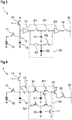
- FIG. 1 shows a schematic of an exemplary embodiment of a pixel 1 according to the improved concept.
- the pixels comprises a photosensitive element 10 for generating an electrical signal that depends on electromagnetic radiation that is incident on the photosensitive elements 10 and generates charges within the latter based on the photoelectric effect.
- the photosensitive element 10 is a photodiode, in particular a pinned photodiode.
- the pixel 1 further comprises a transfer gate 11 and a sense node 12, wherein the transfer gate 11 is connected between the photosensitive element 10 and the sense node 12.
- the transfer gate 11 is configured to provide an electrical connection between the photosensitive element 10 and the sense node 12 upon receiving a particular control signal that opens the transfer gate 11.
- the sense node 12 often also referred to as a floating diffusion, is a node that is electrically isolated from other nodes of the pixel.
- a floating diffusion is realized by a quasi-neutral region that is isolated by p-n junctions. Thus, its potential is determined exclusively by the amount of charge stored in it, and its capacitance. The latter can be determined by means of a floating diffusion capacitance 15.
- the pixel 1 further comprises a reset switch 14 for resetting the sense node 12 and/or the photosensitive element 10 to a predetermined voltage or potential.
- the photosensitive element 10 is reset to a specific voltage before an exposure.
- the sense node 12 is reset to a specific voltage before charges and transferred from the photosensitive element 10 through the transfer gate 11 and after charges are transferred from the sense node 12 to the sampling structure 20.
- the pixel 1 comprises a first buffer amplifier 13, typically also referred to as a source follower, that is connected to the sense node 12.
- the first buffer amplifier 13 is configured to amplify the often small signal of the sense node 12 before providing said signal to the sampling structure 20.
- the sample structure 20 comprises a first sample stage 21 and a second sample stage 22 connected in a series configuration.
- the sample stages 21, 22 in this embodiment each comprise a storage capacitor for storing electric signals as a capacitance.
- the sample structure 20 further comprises a first sample switch S1 and a second sample switch S2 for selectively operating the first and the second sample stages 21, 22.
- the first sample switch S1 is in a closed state while the second sample switch S2 is in an open state when a signal is to be transferred from the sense node 12 to the first sample stage 21.
- both the first and the second sample switches S1, S2 are in a closed state when a signal is to be transferred from the sense node 12 to the second sample stage 22.
- both sample stages 21, 22 have an electrical connection to the first buffer amplifier 13 and thus to the sense node 12, and effective total capacitance that is different from a capacitance of the second sample stage 22 has to be taken into account, particularly when reading out and further processing the signals from the first and the second sample stages.
- the sample structure further comprises a second buffer amplifier 23 for further amplifying signals read out from the first and the second sample stages 21, 22 before providing them to an evaluation circuit via a readout switch 16 and a column line 30 of the pixel 1.
- the pixel 1 is controlled in synchronization with a light source for acquiring an image and enabling background light cancellation.
- the pixel 1 can be operated as follows:
- this readout operation is performed row-by-row sequentially by scanning over the array of pixels 1, wherein this can be achieved without disturbing the signal stored on the photosensitive element 10 of each pixel 1.
- the described order can be alternated particularly in terms of the exposures.
- the first exposure can be performed with the light source having enabled light emission
- the second exposure is the described background light exposure.
- the two exposures can both be performed with enabled light emission of the light source, e.g. at different output powers.
- Figure 2 shows a schematic of an exemplary embodiment of a pixel 1 that is similar to that of figure 1 .
- the first and the second buffer amplifiers 13, 23 as well as the reset switch 16 are shown to be realized as transistors, a common choice for switches employed in pixels.
- the pixel 1 in this embodiment further comprises a precharge transistor 17 that is configured as a load transistor and acts as a current source for the first buffer amplifier 13.
- the precharge transistor 17 may be used to discharge one or both of the storage capacitors of the first and second sample stages 21, 22 of the sampling structure 20 before sampling of the voltage signal from the floating diffusion 12.
- Figures 3 and 4 show exemplary embodiments of a pixel 1 according to the improved concept, wherein the sampling structure 20 comprises a first and a second sample stage 21, 22 that are arranged in a parallel configuration in contrast to the serial configuration of figures 1 and 2 .
- the sampling structure comprises additional first and second readout switches R1, R2 for transferring the respective charges from the storage capacitors of the first and the second sample stages 21, 22 via the second buffer amplifier 23 and the readout switch 16 to the column output 30.
- the two sample stages 21, 22 can be selectively and independently operated without having the charge transfer of the serial configuration described above.
- this configuration simplifies a background cancellation process at the cost of additional components, i.e. transistors.
- the above-mentioned operation principle can be applied also to alternative pixel architectures that are characterized by additional components, such as additional photosensitive elements 10 or transistors, however, comprising at least two sample stages that are selectively operable.
- additional components such as additional photosensitive elements 10 or transistors, however, comprising at least two sample stages that are selectively operable.
- the above-mentioned operation principle can be applied to various architectures that are based on or derived from 3T (three transistor) and 4T (four transistor) pixel architectures.
- Figures 5 and 6 show timing diagrams for illustrating the working principle of a pixel according to the improved concept performing two exposures for enabling a background cancellation process by synchronizing the exposures with an illuminating light source.
- the timing diagram of Figure 5 shows the control signals applied to the different elements of a pixel as shown in figures 1 and 2 as well as to a light source, e.g. a camera flash or a laser diode.
- a light source e.g. a camera flash or a laser diode.
- the x-axis constitutes the time, while on the y-axis the control signals applied to the individual elements are displayed in a stacked manner.
- Each control signal can be understood as a signal with two discrete levels, on and off, up or down, 1 or 0.
- the dashed lines delineate three phases of the pixel operation.
- a first exposure is performed, during which the emission of the light source is disabled, i.e. it is switched off.
- a second exposure is performed, during which the emission of the light source is enabled, i.e. it is switched on and outputs light at a certain output power.
- the signals from the two exposures stored within the first and second sample stages are read out.
- an initial pulsing of the transfer gate 11 and the reset switch 14 before the first exposure by means of a RST and TX pulse of the control signal initiates a predefined starting state of the photosensitive element 10 and of the sense node 12.
- the closing of the transfer gate 11 and the reset switch 14 marks the beginning of the first exposure phase.
- emission of the light source here a laser, e.g. a laser emitting in the infrared domain at around 940 nm for facial recognition purposes, is disabled.
- a further pulsing of the reset switch 14 by means of a RST pulse ensures that the sense node 12 indeed is put in its initial state.
- the TX pulsing of the transfer gate 11 during the "laser off” phase marks the end of the period, in which charges are being integrated within the photosensitive device 10, and charges are transferred from the photosensitive element 10 to the sense node 12.
- both sample switches S1 and S2 are pulsed in order to transfer the charges from the sense node 12 via the first buffer amplifier 13 to the storage capacitor of the second sample stage 22.
- the second sample switch S2 is being opened and the photosensitive element 10 and the sense node 12 are once again reset to the initial state.
- the closing of the transfer gate 11 and the reset switch 14 now marks the beginning of the second exposure phase. During this entire phase, emission of the light source is enabled. A further pulsing up the reset switch 14 by means of a RST pulse ensures once again that the sense node 12 indeed is put in its initial state.
- the TX pulsing of the transfer gate 11 during the "laser on” phase marks the end of the second period, in which charges are being integrated within the photosensitive device 10, and charges are transferred from the photosensitive elements 10 to the sense node 12.
- the steps of the two exposure phases is defined as a global signal, as the described steps are performed simultaneously on a plurality of pixels 1 of an image sensor, for instance.
- both exposure periods constitute a global shutter exposure of the pixel array.
- the readout switch 16 is pulsed by means of a RS pulse of the control signal in order to read out the photo signals stored on the storage capacitor of the second sample stage 22 via the second buffer amplifier 23 and the column line 30. Subsequently, a pulse is applied to the second sample switch S2 for transferring the photo signals stored on the storage capacitor the first sample stage 21. The closing of the readout switch 16 of a respective row of pixels 1 then initiates the readout of the next row of pixels 1 in a corresponding manner. This is indicated in figure 5 by the number in brackets denoting the row number starting from zero to n for a pixel array with n rows.
- readout circuitry arranged either before or after the column line 30 may further process the two signals readout from each pixel by performing a background light cancellation process as described above, for instance.
- the timing diagram of Figure 6 shows the control signals applied to the different elements of a pixel as shown in figures 3 and 4 , having the first and the second sample stages 21, 22 arranged in a parallel configuration, as well as to a light source.
- the proposed storage of two photo signals from exposures at different illumination conditions combined with the readout mechanism as described can be generally applied to conventional pixel architectures having two storage nodes without any changing at device level except for the synchronization with a light source.
- the procedure for the two exposure phases remains the same.
- the RT phase varies slightly from that shown in figure 5 .
- the readout switch 16 is opened and the first and the second readout switches R1, R2 are opened sequentially for the above-mentioned separate readout.
Landscapes
- Engineering & Computer Science (AREA)
- Multimedia (AREA)
- Signal Processing (AREA)
- Transforming Light Signals Into Electric Signals (AREA)
Priority Applications (5)
| Application Number | Priority Date | Filing Date | Title |
|---|---|---|---|
| EP20182563.5A EP3930309A1 (de) | 2020-06-26 | 2020-06-26 | Pixel und verfahren zum betrieb eines pixels |
| DE112021003421.9T DE112021003421T5 (de) | 2020-06-26 | 2021-06-17 | Pixel und Verfahren zum Betreiben eines Pixels |
| CN202180042703.9A CN115804102B (zh) | 2020-06-26 | 2021-06-17 | 像素元件和用于操作像素元件的方法 |
| PCT/EP2021/066353 WO2021259744A1 (en) | 2020-06-26 | 2021-06-17 | Pixel and method for operating a pixel |
| US18/002,413 US12375832B2 (en) | 2020-06-26 | 2021-06-17 | Pixel, electric device and method having a transfer gate and sample stages configured to be operated in conjunction with a light source in response to a control signal |
Applications Claiming Priority (1)
| Application Number | Priority Date | Filing Date | Title |
|---|---|---|---|
| EP20182563.5A EP3930309A1 (de) | 2020-06-26 | 2020-06-26 | Pixel und verfahren zum betrieb eines pixels |
Publications (1)
| Publication Number | Publication Date |
|---|---|
| EP3930309A1 true EP3930309A1 (de) | 2021-12-29 |
Family
ID=71266298
Family Applications (1)
| Application Number | Title | Priority Date | Filing Date |
|---|---|---|---|
| EP20182563.5A Withdrawn EP3930309A1 (de) | 2020-06-26 | 2020-06-26 | Pixel und verfahren zum betrieb eines pixels |
Country Status (5)
| Country | Link |
|---|---|
| US (1) | US12375832B2 (de) |
| EP (1) | EP3930309A1 (de) |
| CN (1) | CN115804102B (de) |
| DE (1) | DE112021003421T5 (de) |
| WO (1) | WO2021259744A1 (de) |
Cited By (4)
| Publication number | Priority date | Publication date | Assignee | Title |
|---|---|---|---|---|
| WO2023152035A1 (en) * | 2022-02-09 | 2023-08-17 | Ams Sensors Belgium Bvba | Image sensor, optoelectronic device including the image sensor and method for operating the image sensor |
| WO2024054544A1 (en) * | 2022-09-08 | 2024-03-14 | ams Sensors USA Inc. | Pixel arrangement on two substrates and method for fabricating an image sensor |
| WO2024158634A1 (en) * | 2023-01-23 | 2024-08-02 | ams Sensors USA Inc. | Pixel arrangement with two transfer transistors and method for operating the pixel arrangement |
| US12604114B2 (en) | 2022-02-09 | 2026-04-14 | Ams Sensors Belgium Bvba | Imaging device, optoelectronic device and method for operating an imaging device |
Families Citing this family (1)
| Publication number | Priority date | Publication date | Assignee | Title |
|---|---|---|---|---|
| US12126928B2 (en) * | 2022-12-29 | 2024-10-22 | BAE Systems Imaging Solutions Inc. | Column readout amplifier for image sensors |
Citations (2)
| Publication number | Priority date | Publication date | Assignee | Title |
|---|---|---|---|---|
| EP2109306A2 (de) * | 2008-04-07 | 2009-10-14 | CMOSIS nv | Pixelarray mit globaler Blende |
| US20170013210A1 (en) * | 2014-08-28 | 2017-01-12 | Pixart Imaging Inc. | Image sensor and imaging system adopting analog buffer |
Family Cites Families (5)
| Publication number | Priority date | Publication date | Assignee | Title |
|---|---|---|---|---|
| WO2014055391A2 (en) | 2012-10-05 | 2014-04-10 | Rambus Inc. | Conditional-reset, multi-bit read-out image sensor |
| US20170366766A1 (en) * | 2016-06-16 | 2017-12-21 | Semiconductor Components Industries, Llc | Image sensors having high dynamic range functionalities |
| GB2574619B (en) * | 2018-06-12 | 2022-10-12 | Res & Innovation Uk | Image sensor |
| EP3605606B1 (de) * | 2018-08-03 | 2022-06-15 | ams Sensors Belgium BVBA | Bildgebungssystem mit einer infrarotlichtquelle und einem bildsensor |
| KR102895535B1 (ko) * | 2019-11-27 | 2025-12-05 | 삼성전자주식회사 | 이미지 센서, 그것을 포함하는 이미지 장치, 및 그것의 동작 방법 |
-
2020
- 2020-06-26 EP EP20182563.5A patent/EP3930309A1/de not_active Withdrawn
-
2021
- 2021-06-17 DE DE112021003421.9T patent/DE112021003421T5/de active Pending
- 2021-06-17 WO PCT/EP2021/066353 patent/WO2021259744A1/en not_active Ceased
- 2021-06-17 CN CN202180042703.9A patent/CN115804102B/zh active Active
- 2021-06-17 US US18/002,413 patent/US12375832B2/en active Active
Patent Citations (2)
| Publication number | Priority date | Publication date | Assignee | Title |
|---|---|---|---|---|
| EP2109306A2 (de) * | 2008-04-07 | 2009-10-14 | CMOSIS nv | Pixelarray mit globaler Blende |
| US20170013210A1 (en) * | 2014-08-28 | 2017-01-12 | Pixart Imaging Inc. | Image sensor and imaging system adopting analog buffer |
Cited By (6)
| Publication number | Priority date | Publication date | Assignee | Title |
|---|---|---|---|---|
| WO2023152035A1 (en) * | 2022-02-09 | 2023-08-17 | Ams Sensors Belgium Bvba | Image sensor, optoelectronic device including the image sensor and method for operating the image sensor |
| US12549870B2 (en) | 2022-02-09 | 2026-02-10 | Ams Sensors Belgium Bvba | Imaging device, optoelectronic device and method for operating an imaging device |
| US12604114B2 (en) | 2022-02-09 | 2026-04-14 | Ams Sensors Belgium Bvba | Imaging device, optoelectronic device and method for operating an imaging device |
| WO2024054544A1 (en) * | 2022-09-08 | 2024-03-14 | ams Sensors USA Inc. | Pixel arrangement on two substrates and method for fabricating an image sensor |
| WO2024158634A1 (en) * | 2023-01-23 | 2024-08-02 | ams Sensors USA Inc. | Pixel arrangement with two transfer transistors and method for operating the pixel arrangement |
| TWI895942B (zh) * | 2023-01-23 | 2025-09-01 | 美商Ams傳感器美國公司 | 具有二傳輸電晶體之像素配置、圖像感測器及用於操作像素配置之方法 |
Also Published As
| Publication number | Publication date |
|---|---|
| US20230232132A1 (en) | 2023-07-20 |
| WO2021259744A1 (en) | 2021-12-30 |
| US12375832B2 (en) | 2025-07-29 |
| CN115804102B (zh) | 2025-08-12 |
| DE112021003421T5 (de) | 2023-04-27 |
| CN115804102A (zh) | 2023-03-14 |
Similar Documents
| Publication | Publication Date | Title |
|---|---|---|
| US12375832B2 (en) | Pixel, electric device and method having a transfer gate and sample stages configured to be operated in conjunction with a light source in response to a control signal | |
| US12096140B2 (en) | Self calibrating barrier modulation pixel | |
| US9100605B2 (en) | Global shutter with dual storage | |
| US20180176498A1 (en) | Global shutter pixel structures with shared transfer gates | |
| TW201911855A (zh) | 具有堆疊基板的光感測器的偵測電路 | |
| CN111684791B (zh) | 像素结构、具有像素结构的图像传感器装置和系统、以及操作该像素结构的方法 | |
| US12549870B2 (en) | Imaging device, optoelectronic device and method for operating an imaging device | |
| US10051216B2 (en) | Imaging apparatus and imaging method thereof using correlated double sampling | |
| US10063796B2 (en) | Sensing pixel having sampling circuitry to sample photodiode signal multiple times before reset of photodiode | |
| TW201630409A (zh) | 用以增加像素靈敏度及動態範圍之方法及裝置 | |
| US12604114B2 (en) | Imaging device, optoelectronic device and method for operating an imaging device | |
| CN117813835A (zh) | 像素装置、图像传感器和操作像素装置的方法 | |
| JP2022522952A (ja) | 飛行時間型装置および3d光学検出器 | |
| EP3445039B1 (de) | Detektionsschaltung für fotosensor mit gestapelten substraten | |
| CN118414840A (zh) | 像素装置、像素矩阵、图像传感器和操作像素装置的方法 | |
| CN119031258B (zh) | 像素模块、光电传感模组和相机 | |
| KR20190108374A (ko) | 이미지 센싱 장치 및 이를 이용한 디스플레이 장치 | |
| EP4681441A1 (de) | Pixelanordnung, abbildungsvorrichtung und verfahren zum betreiben einer pixelanordnung | |
| CN117795976A (zh) | 像素布局、图像传感器和操作像素布局的方法 |
Legal Events
| Date | Code | Title | Description |
|---|---|---|---|
| PUAI | Public reference made under article 153(3) epc to a published international application that has entered the european phase |
Free format text: ORIGINAL CODE: 0009012 |
|
| STAA | Information on the status of an ep patent application or granted ep patent |
Free format text: STATUS: THE APPLICATION HAS BEEN PUBLISHED |
|
| AK | Designated contracting states |
Kind code of ref document: A1 Designated state(s): AL AT BE BG CH CY CZ DE DK EE ES FI FR GB GR HR HU IE IS IT LI LT LU LV MC MK MT NL NO PL PT RO RS SE SI SK SM TR |
|
| B565 | Issuance of search results under rule 164(2) epc |
Effective date: 20201119 |
|
| STAA | Information on the status of an ep patent application or granted ep patent |
Free format text: STATUS: THE APPLICATION IS DEEMED TO BE WITHDRAWN |
|
| 18D | Application deemed to be withdrawn |
Effective date: 20220630 |