EP3933367A1 - Sensorschnittstellenschaltung, sensorsystem und verfahren zur signalmessung - Google Patents
Sensorschnittstellenschaltung, sensorsystem und verfahren zur signalmessung Download PDFInfo
- Publication number
- EP3933367A1 EP3933367A1 EP20305583.5A EP20305583A EP3933367A1 EP 3933367 A1 EP3933367 A1 EP 3933367A1 EP 20305583 A EP20305583 A EP 20305583A EP 3933367 A1 EP3933367 A1 EP 3933367A1
- Authority
- EP
- European Patent Office
- Prior art keywords
- circuit
- filter
- time
- chopper
- continuous
- Prior art date
- Legal status (The legal status is an assumption and is not a legal conclusion. Google has not performed a legal analysis and makes no representation as to the accuracy of the status listed.)
- Granted
Links
Images


Classifications
-
- G—PHYSICS
- G01—MEASURING; TESTING
- G01R—MEASURING ELECTRIC VARIABLES; MEASURING MAGNETIC VARIABLES
- G01R27/00—Arrangements for measuring resistance, reactance, impedance, or electric characteristics derived therefrom
- G01R27/02—Measuring real or complex resistance, reactance, impedance, or other two-pole characteristics derived therefrom, e.g. time constant
- G01R27/26—Measuring inductance or capacitance; Measuring quality factor, e.g. by using the resonance method; Measuring loss factor; Measuring dielectric constants ; Measuring impedance or related variables
- G01R27/2605—Measuring capacitance
-
- G—PHYSICS
- G01—MEASURING; TESTING
- G01L—MEASURING FORCE, STRESS, TORQUE, WORK, MECHANICAL POWER, MECHANICAL EFFICIENCY, OR FLUID PRESSURE
- G01L9/00—Measuring steady of quasi-steady pressure of fluid or fluent solid material by electric or magnetic pressure-sensitive elements; Transmitting or indicating the displacement of mechanical pressure-sensitive elements, used to measure the steady or quasi-steady pressure of a fluid or fluent solid material, by electric or magnetic means
- G01L9/12—Measuring steady of quasi-steady pressure of fluid or fluent solid material by electric or magnetic pressure-sensitive elements; Transmitting or indicating the displacement of mechanical pressure-sensitive elements, used to measure the steady or quasi-steady pressure of a fluid or fluent solid material, by electric or magnetic means by making use of variations in capacitance, i.e. electric circuits therefor
- G01L9/125—Measuring steady of quasi-steady pressure of fluid or fluent solid material by electric or magnetic pressure-sensitive elements; Transmitting or indicating the displacement of mechanical pressure-sensitive elements, used to measure the steady or quasi-steady pressure of a fluid or fluent solid material, by electric or magnetic means by making use of variations in capacitance, i.e. electric circuits therefor with temperature compensating means
-
- G—PHYSICS
- G01—MEASURING; TESTING
- G01P—MEASURING LINEAR OR ANGULAR SPEED, ACCELERATION, DECELERATION, OR SHOCK; INDICATING PRESENCE, ABSENCE, OR DIRECTION, OF MOVEMENT
- G01P15/00—Measuring acceleration; Measuring deceleration; Measuring shock, i.e. sudden change of acceleration
- G01P15/02—Measuring acceleration; Measuring deceleration; Measuring shock, i.e. sudden change of acceleration by making use of inertia forces using solid seismic masses
- G01P15/08—Measuring acceleration; Measuring deceleration; Measuring shock, i.e. sudden change of acceleration by making use of inertia forces using solid seismic masses with conversion into electric or magnetic values
- G01P15/125—Measuring acceleration; Measuring deceleration; Measuring shock, i.e. sudden change of acceleration by making use of inertia forces using solid seismic masses with conversion into electric or magnetic values by capacitive pick-up
-
- G—PHYSICS
- G01—MEASURING; TESTING
- G01D—MEASURING NOT SPECIALLY ADAPTED FOR A SPECIFIC VARIABLE; ARRANGEMENTS FOR MEASURING TWO OR MORE VARIABLES NOT COVERED IN A SINGLE OTHER SUBCLASS; TARIFF METERING APPARATUS; MEASURING OR TESTING NOT OTHERWISE PROVIDED FOR
- G01D5/00—Mechanical means for transferring the output of a sensing member; Means for converting the output of a sensing member to another variable where the form or nature of the sensing member does not constrain the means for converting; Transducers not specially adapted for a specific variable
- G01D5/12—Mechanical means for transferring the output of a sensing member; Means for converting the output of a sensing member to another variable where the form or nature of the sensing member does not constrain the means for converting; Transducers not specially adapted for a specific variable using electric or magnetic means
- G01D5/14—Mechanical means for transferring the output of a sensing member; Means for converting the output of a sensing member to another variable where the form or nature of the sensing member does not constrain the means for converting; Transducers not specially adapted for a specific variable using electric or magnetic means influencing the magnitude of a current or voltage
- G01D5/24—Mechanical means for transferring the output of a sensing member; Means for converting the output of a sensing member to another variable where the form or nature of the sensing member does not constrain the means for converting; Transducers not specially adapted for a specific variable using electric or magnetic means influencing the magnitude of a current or voltage by varying capacitance
Definitions
- the present invention relates generally to sensor technologies. More specifically, the present invention relates to a sensor interface circuit with reduced susceptibility to electromagnetic interference, a sensor system implementing the sensor interface circuit, and a method of signal measurement.
- a capacitive sensor device such as a Coriolis-based gyroscope transducer, an accelerometer, a pressure sensor, and the like, outputs a capacitive signal indicative of measurements or other properties of the capacitive sensor device. Subsequent signal conditioning for such devices can be more efficient by first converting the capacitance signal to an analog voltage signal, processing the analog voltage signal, and converting the analog voltage signal to a digital representation of the signal.
- CMOS complementary metal-oxide-semiconductor
- ASIC application specific integrated circuit
- the input and output pads of the sensor die and the measuring circuit die may be suitably connected by wire bonds. These wire bonds are susceptible to external electromagnetic interference (EMI) that can inject charge (e.g., an interference signal component) into the sense nodes of the sensor which can introduce error into the desired signal.
- EMI external electromagnetic interference
- a sensor interface circuit comprising a continuous-time capacitance-to-voltage (C/V) converter having a C/V input and output ends, the C/V input end being configured for electrical connection with first and second sense nodes of a capacitive sensor; a filter circuit having first and second resistors at corresponding first and second filter input ends of the filter circuit, a capacitor connected between first and second filter output ends of the filter circuit, and a chopper circuit interposed between the first and second filter input ends and the first and second filter output ends, wherein the C/V output end of the continuous-time C/V converter is electrically coupled to the first and second filter input ends of the filter circuit; and a buffer circuit electrically coupled with the first and second filter output ends of the filter circuit.
- C/V capacitance-to-voltage
- the first and second resistors (410, 412) and the capacitor (414) of the filter circuit (306) may constitute a passive anti-aliasing filter (312).
- a method comprising receiving, at a continuous-time capacitance-to-voltage (C/V) converter, first and second sense signals from a capacitive sensor; generating, at the continuous-time C/V converter, a raw voltage signal in response to the first and second sense signals, each of the first and second sense signals including an interference signal component, and the raw voltage signal including the interference signal component; attenuating the interference signal component in the raw voltage signal at a filter circuit to produce a filtered voltage signal; and following attenuation of the interference signal component, down-converting the filtered voltage signal to produce a baseband analog data stream.
- C/V capacitance-to-voltage
- a sensor system comprising a first die having a capacitive sensor implemented thereon, the capacitive sensor having a first sense node and a second sense node; and a second die, having a continuous-time capacitance-to-voltage (C/V) converter, a filter circuit, and a buffer circuit implemented thereon, wherein the continuous-time C/V converter has C/V input and output ends, the C/V input end being configured for electrical connection with the first and second sense nodes of the capacitive sensor, the continuous-time C/V converter comprising a continuous-time gain stage implemented with a capacitor feedback stage, and further implemented with a direct current (DC) feedback circuit, wherein the DC feedback circuit is configured to set a DC bias for the continuous-time gain stage; the filter circuit has first and second resistors at corresponding first and second filter input ends of the filter circuit, a capacitor connected between a first and second filter output ends of the filter circuit, and a chopper circuit interposed between the first and second filter input ends and the first and
- the present disclosure concerns a sensor interface circuit, a sensor system, and a method of signal measurement.
- the sensor interface circuit includes a continuous-time capacitance-to-voltage (C/V) converter and a passive anti-aliasing filter (AAF), in which the AAF is added around an output chopper circuit.
- C/V capacitance-to-voltage
- AAF passive anti-aliasing filter
- a sensor output signal from a capacitive sensor is first sampled by an active sample-and-hold circuit at the input to an analog-to-digital converter after filtering at the AAF.
- the output chopper circuit is interposed between the resistors and a capacitor of the AAF so that the raw voltage signal from the continuous-time C/V is filtered before the chopping operation (e.g., demodulation).
- the high-frequency interference components in the raw voltage signal may be attenuated before down-conversion.
- the bandwidth of the AAF may not attenuate signals in the signal band of interest, which at the output of the continuous-time C/V, is a small band of frequencies around the chopper frequency. Consequently, the architecture of the sensor interface circuit may have reduced susceptibility to electromagnetic interference, therefore resulting in less error in the desired signal.
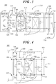
- FIG. 1 shows in a simplified and representative form a block diagram of a sensor system 100.
- sensor system 100 includes an excitation circuit 102 electrically coupled to a capacitive sensor 104, and a measuring circuit 106 electrically coupled to capacitive sensor 104.
- Capacitive sensor 104 may be a Coriolis-based gyroscope transducer, an accelerometer, a pressure sensor, and the like, that outputs capacitive signals indicative of measurements or other properties of an external stimulus.
- Excitation circuit 102 is configured to excite capacitive sensor 104 by applying an excitation waveform, V EX , 108 to capacitive sensor 104.
- measuring circuit 106 is configured to measure results from the excitation. That is, excitation results in the form of a first charge signal, referred to herein as a first sense signal 110 (Q P ) and a second charge signal, referred to herein as a second sense signal 112 (Q N ), in response to a physical stimulus.
- First and second sense signals 110, 112 are conveyed to measuring circuit 106 from capacitive sensor 104.
- Measuring circuit 106 generally includes a signal chain (discussed below) that is used to process first and second sense signals 110, 112 from capacitive sensor 104. In an embodiment, measuring circuit 106 may therefore output a desired digital data stream (e.g., a digital sense signal 114, labeled ADC OUT ). Digital sense signal 114 is indicative of the stimulus being sensed.
- FIG. 2 shows in a simplified and representative form a side view of a packaged sensor system 200 that includes a sensor die 202 and an application specific integrated circuit (ASIC) die 204.
- excitation circuit 102 and measuring circuit 106 may be implemented on one or more application specific integrated circuits (ASIC) separate from capacitive sensor 104.
- ASIC application specific integrated circuits
- capacitive sensor 104 may be implemented in a first die, e.g., sensor die 202
- excitation and measuring circuits 102 and 106 may be implemented in a second die, e.g., ASIC die 204.
- Bond wires 206 suitably interconnect sensor die 202 with ASIC die 204, as will be discussed in greater detail below.
- EMI electromagnetic interference
- bond wires 206 that connect sensor die 202 to ASIC die 204 can inject charge into the sense nodes of capacitive sensor 104.
- the frequency of the EMI may span from tens of kilohertz to hundreds of megahertz.
- the charge amplifier e.g., a charge-to-voltage converter
- the charge amplifier in measuring circuit 106 may be a discrete-time system, implemented with switched-capacitor circuits.
- the charge from capacitive sensor 104 is collected by the charge amplifier feedback capacitance and is converted to a discrete-time voltage signal.
- the sampling nature of the charge amplifier may alias the high-frequency interference within the signal frequency band.
- demodulation chopper circuits may be employed in measuring circuit 106 when an excitation chopper (also referred to as a modulation chopper) is implemented to reject the charge amplifier low-frequency noise and offset, and leakage on the sense nodes of capacitive sensor 104.
- a demodulation chopper following the charge amplifier may translate the interference into the signal frequency band, which cannot be removed by subsequent low-pass filtering.
- chopper circuits may provide efficient frequency translation.
- Embodiments disclosed herein entail an sensor interface circuit that applies low-pass filtering prior to any sampling or demodulation operations to reduce the amount of high-frequency interference translating into the signal band. Additionally, the circuitry can interface to a conventional analog-to-digital converter.
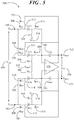
- FIG. 3 shows a block diagram of a sensor system 300 in accordance with an embodiment.
- Sensor system 300 includes a first die (e.g., sensor die 202, FIG. 2 ) having a capacitive sensor 302 implemented thereon and a second die (e.g., ASIC die 204, FIG. 2 ) having a continuous-time capacitance-to-voltage (C/V) converter 304 (labeled CT C/V), a filter circuit 306 (labeled AAF/CHOPPER), and a buffer circuit 308 (labeled S/H) implemented thereon.
- C/V capacitance-to-voltage
- continuous-time C/V converter 304, filter circuit 306, and buffer circuit 308 constitute an analog frontend, e.g., a sensor interface circuit 310, of sensor system 300.
- filter circuit 306 includes a low pass filter, referred to herein as an anti-aliasing filter 312, added around a chopper circuit 314.
- filter circuit 306 is collectively labeled AAF/CHOPPER.
- ADC analog-to-digital converter 316
- an excitation circuit (e.g., excitation circuit 102, FIG. 1 ) may be implemented on the second die or on another die separate from the second die.
- Capacitive sensor 302 may be any of a variety of capacitive transducers which may be configured to sense a desired stimulus (e.g., pressure, acceleration, angular velocity, and so forth).
- capacitive sensor 302 may be a parallel-plate electrode in which one of the plates is movable relative to the other plate, with variable gaps being formed between the fixed and movable plates.
- capacitive sensor 302 may include first and second sense nodes 318, 320, and a third node interposed between first and second sense nodes 318, 320 and referred to herein as a middle node 322.
- Capacitive sensor 302 is configured to produce a first charge signal, referred to herein as a first sense signal 324 and labeled Q P , at first sense node 318 and is configured to produce a second charge signal, referred to herein as a second sense signal 326 and labeled Q N , at second sense node 320.
- Middle node 322 is configured to receive an alternating voltage waveform, e.g., an excitation voltage 328, labeled V EX .
- Excitation voltage 328 is produced, for example, at an input chopper or mixer (not shown) of an excitation circuit (e.g., excitation circuit 102, FIG. 1 ).
- excitation voltage 328 is configured to charge the capacitors of capacitive sensor 302 and up-convert first and second sense signals 320, 322 to a chopper fundamental frequency of chopper circuit 314.
- the width of the variable gaps between the fixed and movable plates of capacitive sensor 302 change, which in turn causes first and second sense signals 324, 326 to change.
- Bond wires 330 electrically connect first and second sense nodes 318, 320 of capacitive sensor 302 on the first die (e.g., sensor die 202) to a C/V input end 332 of continuous-time C/V converter 304 of the second die (e.g., ASIC die 204).
- C/V input end 332 includes a first input node 334 and a second input node 336.
- One of bond wires 330 connects first input node 334 to first sense node 318 of capacitive sensor 302 and another one of bond wires 330 connects second input node 336 to second sense node 320 of capacitive sensor 302.
- EMI 338 (represented by a lightning bolt) terminating on bond wires 330 can inject charge into first and second sense nodes 318, 320 of capacitive sensor 302 such that first and second sense signals 324, 326 may include an interference signal component resulting from EMI 338.
- the energy from EMI 338 does not symmetrically inject charge error into first and second sense nodes 318, 320. That is, the source of EMI 338 is not necessarily equidistant from first and second sense nodes 318, 320, and even if the source of EMI 338 is equidistant from first and second sense nodes 318, 320, the parasitic capacitances around first and second sense nodes 318, 320 is not equivalent.
- Interface circuit 310 effectively forms a signal chain to process first and second sense signals 324, 326 and to attenuate the interference signal component from first and second sense signals 324, 326.
- Continuous-time C/V converter 304 receives the charge signal (e.g., first and second sense signals 324, 326) at C/V input end 332 and converts the charge signal from capacitive sensor 302 into a raw voltage signal 340, labeled V R .
- Raw voltage signal 340 may be considered a continuous signal, or equivalently, a continuous-time signal or an analog signal. That is, raw voltage signal 340 is a signal that will have some value at every instant in time. In contrast, a discrete-time signal has a values occurring at distinct, separate "points in time.” Thus, a signal that is sampled or measured at a particular sampling frequency may be considered a discrete-time signal.
- Continuous-time C/V converter 304 can include a continuous-time gain stage 342 implemented with a capacitor feedback stage 344 (e.g., two capacitor feedback stages 344 in this differential circuit example).
- a capacitor feedback stage 344 e.g., two capacitor feedback stages 344 in this differential circuit example.
- continuous-time C/V converter 304 may be implemented with a DC feedback circuit 346 (e.g., two DC feedback circuits 346 in this differential circuit example).
- a relatively straightforward topology for each of DC feedback circuits 346 may be a resistor connecting a C/V output end 348 of continuous-time C/V converter 304 to C/V input end 332 of continuous-time C/V converter 304.
- Another topology for each of DC feedback circuits 346 may be back-to-back diodes connecting C/V output end 348 of continuous-time C/V converter 304 to C/V input end 332 of continuous-time C/V converter 304 to obtain a relatively high resistance in a small area.
- DC control with an integrator in the feedback path of each DC feedback circuit 346 may alternatively be implemented due to the potential for leakage current on capacitive sensor 302. Accordingly, it should be understood that various suitable options for DC feedback circuit 346 may be implemented with continuous-time C/V converter 304.
- FIG. 4 shows a schematic diagram of filter circuit 306 of sensor system 300.
- First and second C/V output nodes 400, 402 at C/V output end 348 of continuous-time C/V converter 304 are electrically coupled with first and second filter input nodes 404, 406 at a filter input end 408 of filter circuit 306.
- Filter circuit 306 includes first and second resistors 410, 412 (labeled R1 AAF and R2 AAF ) at corresponding first and second filter input nodes 404, 406 of filter circuit 306 and a capacitor 414 (labeled C AAF ) coupled between first and second filter output nodes 416, 418 at a filter output end 420 of filter circuit 306.
- first and second resistors 410, 412 and capacitor 414 of filter circuit 306 constitute the passive anti-aliasing filter 312.
- Chopper circuit 314 of filter circuit 306 is interposed between filter input end 408 and filter output end 420. More particularly, first resistor 410 is connected between first filter input node 404 and a first chopper input node 422 and second resistor 412 is connected between second filter input node 406 and a second chopper input node 424. A first chopper output node 426 is electrically connected to first filter output node 416 and a second chopper output node 428 is electrically connected to second filter output node 418.
- Chopper circuit 314 receives a first chopper clock signal 430 ( ⁇ CH1 ) and a second chopper clock signal 432 (( ⁇ CH2 ).
- first chopper clock signal 430 denotes one phase of chopper circuit 314 (e.g., a positive phase)
- second chopper clock signal 432 denotes the other phase of chopper circuit 314 (e.g., a negative phase).
- First and second chopper clock signals 430 and 432 are not asserted at the same time.
- chopper circuit 314 yields a baseband analog data stream 434, V CH , at both a positive chopping phase and a negative chopping phase.
- chopper circuit 314 (sometimes referred to as an output chopper or output mixer) frequency chops, or down-converts, raw analog voltage 340 back to the baseband frequency (i.e., shifts the signal band frequency by the fundamental chopper frequency). Placing chopper circuit 314 between the resistor (i.e., first and second resistors 410, 412) and the capacitor (i.e., capacitor 414) of anti-aliasing filter 312 serves two purposes.
- raw voltage signal 340 from continuous-time C/V converter 304 is filtered prior to the chopping operation so that high-frequency interference signal components in raw voltage signal 340 may be attenuated (i.e., diminished) to produce a filtered voltage signal 436, V F , before down-conversion.
- the bandwidth of anti-aliasing filter 312 does not attenuate raw voltage signal 340 in the signal band of interest, which at C/V output end 348, is a small band of frequencies around the fundamental chopper frequency.
- baseband analog data stream 434 in which the interference signal component is attenuated prior to down-conversion is output from filter circuit 306 at first and second filter output nodes 404, 406 of filter circuit 306. Accordingly, continuous-time C/V converter 304 passes the interference signal component in raw voltage signal 340 to anti-aliasing filter 312 without sampling. Anti-aliasing filter 312 reduces the amplitude of high-frequency components, especially at odd harmonics of the chopper fundamental frequency that would otherwise translate to baseband. The first sampling instant is therefore after filtering and chopping at filter circuit 306.
- ADC 316 has an ADC input end 350 coupled to a buffer output end 352 of buffer circuit 308.
- ADC 316 may be configured to convert discrete-time analog voltage values (discussed below) output from buffer circuit 308 to a digital data stream 354.
- buffer circuit 308 between filter circuit 306 and ADC 316 protects the signal charge on capacitor 414 of anti-aliasing filter 312 from transferring to a sampling capacitor 356 of ADC 316, which could otherwise attenuate the signal.
- FIG. 5 shows a schematic diagram of buffer circuit 308 of sensor system 300 ( FIG. 3 ).
- Buffer circuit 308 performs a filtered, sample-and-hold function. That is, buffer circuit 308 is configured to sample chopped output voltage 434 from filter circuit 306 ( FIG. 3 ) without degrading the signal charge on the anti-aliasing filter capacitance, filter the chopper fundamental frequency and harmonics, and enable connection to ADC 316 ( FIG. 3 ).
- Buffer circuit 308 includes a positive voltage input node 500 and a negative voltage input node 502 configured to receive the positive and negative phases (V IN-P and V IN-N ) which together form chopped output voltage 434.
- buffer circuit 308 includes a phase one clock 504 ( ⁇ f 1 ), a phase two clock 506 ( ⁇ f 2 ), a delayed phase one clock 508 ( ⁇ f 1D ), a delayed phase two clock 510 ( ⁇ f 2D ), first input sampling capacitors 512 (C SH1A ), second input sampling capacitors 514 (C SH1B ), feedback capacitors 516 (C SH2 ), a common-mode voltage source 518 (V CM ), and a gain stage 520.
- Buffer circuit 308 further includes a positive voltage output node 522 and a negative voltage output node 524 configured to output positive and negative samples (V SH-P , V SH-N ) that together form discrete-time analog voltage values 526, V SH , that are output from voltage output nodes 522, 524.
- the "D" for the delayed phase one and two clocks 508, 510 refers to a delayed version of the clock.
- delayed phase one clock 508 is delayed as compared to phase one clock 504 by an amount of time on the order of, for example a few nanoseconds.
- delayed phase two clock 510 is delayed as compared to phase two clock 506 on the order of, for example, a few nanoseconds.
- delaying clocks in this fashion may be implemented to reduce signal-dependent charge injection resulting from charge in the channel of a metal-oxide-semiconductor field-effect transistor (MOSFET) switch dispersing when the switch opens.
- MOSFET metal-oxide-semiconductor field-effect transistor
- chopped output voltage 434 is sampled on the first and second input capacitance stages (e.g., first and second input sampling capacitors 512, 514) in one phase and then the charge is combined with the charge on feedback capacitors 516 in another phase by configuring input sampling capacitors 512, 514 in parallel with respective feedback capacitors 516.
- there are two sets of input capacitors e.g., first and second input sampling capacitors 512, 514, to sample both phases of the chopper output, e.g., chopped output voltage 434.
- the fixed feedback capacitors 516 implement a filtering operation.
- the clock frequency is significantly higher than the filter cut-off frequency. Accordingly, the voltage across input sampling capacitors 512, 514 is equivalent to the voltage across feedback capacitors 516 so that when input sampling capacitors 512, 514 are configured to sample the input, e.g. chopped output voltage 434, the capacitance of capacitor 414 ( FIG. 4 ) of anti-aliasing filter 312 of filter circuit 306 is not disturbed.
- FIG. 6 shows a table of a timing diagram 600 for the clocks of chopper and buffer circuits 304, 306 ( FIGs. 3-5 ).
- buffer circuit 306 samples the chopper output (e.g., chopped output voltage 434, FIG. 4 ) on the negative edges of phase one and phase two clocks 504, 506.
- these negative edges occur once near the end of a positive phase 602 of first chopper clock 430 and once near the end of a positive phase 604 of second chopper clock 432. Accordingly, a first sample 606 can be obtained at the negative edge of phase one clock 504 and a second sample 608 can be obtained at the negative edge of phase two clock 506.
- FIG. 7 shows a chart 700 demonstrating attenuation of interference signal components by implementing interface circuit 310 ( FIG. 3 ) of sensor system ( FIG. 3 ) in accordance with an embodiment.
- Continuous-time C/V converter 304 passes high frequency interference signal components 702 without sampling to filter circuit 306.
- Anti-aliasing filter 312 of filter circuit 306 reduces, e.g., attenuates, the amplitude of interference signal components 702 especially at odd harmonics of a chopper fundamental frequency 704.
- the unattenuated portion of interference signal components 702 is represented by dotted line sections 706 and the remaining portion of interference signal components 702 is represented by solid line sections 708.
- chopper circuit 314 which has components at odd multiples of chopper fundamental frequency 704, may down-convert solid line sections 708 of interference signal components 702 to baseband 710, but the resulting in-band error is less. Thereafter, the first sampling instant (e.g., first sample 606, FIG. 6 ) occurs after the filter and chopper operations.
- FIG. 8 shows a block diagram of a sensor system 800 in accordance with another embodiment.
- Sensor system 800 includes a capacitive sensor 802, a continuous-time C/V converter 804, a filter circuit 806, and a buffer circuit 808.
- continuous-time C/V converter 804, filter circuit 806, and buffer circuit 808 constitute an analog frontend, e.g., an interface circuit 810, of sensor system 800.
- Filter circuit 806 includes an anti-aliasing filter 812, added around a chopper circuit 814.
- an analog-to-digital converter 816 (ADC) may additionally be included.
- ADC analog-to-digital converter 816
- Elements 802, 804, 808, 812, 814, and 816 generally correspond with elements 302, 304, 308, 312, 314, and 316 of sensor system 300 of FIG. 3 . Thus, a description of them will not be repeated herein for brevity.
- Chart 700 of FIG. 7 only shows the down-converting of remaining interference 708 of interference signal components 702.
- chopper circuit 314 FIG. 3
- anti-aliasing filter 812 may be considered a first filter
- filter circuit 806 of sensor system 800 further includes a second filter circuit 818 cascaded with the first filter circuit and interposed between anti-aliasing filter 812 and buffer circuit 808.
- filter circuit 806 is labeled AAF1/CHOPPER/AAF2.
- second filter circuit 818 includes third and fourth resistors 820, 822 at corresponding third and fourth input ends 824, 826 of second filter circuit 818 and a second capacitor 828 connected between third and fourth output ends 830, 832 of second filter circuit 818.
- second filter circuit 818 constitutes a passive RC (resistor-capacitor) filter.
- second filter circuit 818 may be configured to have the same cut-off frequency as the first filter circuit, e.g., anti-aliasing filter 812.
- Cascading another passive RC filter e.g., second filter circuit 818, with the same cut-off frequency as the first passive RC filter (e.g., anti-aliasing filter 812) before buffer circuit 808 may contribute to additional attenuation of interference signal components 702.
- FIG. 9 shows a flowchart of a signal measurement process 900 in accordance with another embodiment.
- Signal measurement process 900 may be executed in connection with a sensor system having an interface circuit that includes a continuous-time C/V converter, a filter circuit having an anti-aliasing filter added around an output chopper, and a buffer circuit and/or with a sensor system that further includes a second filter cascaded with the anti-aliasing filter.
- a sensor system 300 described above and shown in FIGs. 3-5 in connection with the following description.
- Signal measurement process 900 demonstrates a single measurement cycle for simplicity. It should be apparent that execution of signal measurement process 900 may be continuously repeated for a multiplicity of measurement cycles.
- Signal measurement process 900 includes a number of process blocks, each of which will be described in detail below. Each process block generically illustrated in FIG. 9 may entail a single process or multiple sub-processes. Furthermore, the process blocks illustrated in FIG. 9 and described below are provided by way of non-limiting example. In alternative embodiments of signal measurement process 900, additional process blocks may be performed, certain process blocks may be omitted, and/or the illustrated process blocks may be performed in alternative sequences.
- an excitation voltage is provided to capacitive sensor (e.g., excitation voltage 328 provided at middle node 322 of capacitive sensor 302).
- sense signals are received at a continuous-time C/V converter from the capacitive sensor (e.g., first and second sense signals 318, 320 are received at first and second input nodes 334, 336 at C/V input end 332 of continuous-time C/V converter 304 of interface circuit 310).
- a raw voltage signal is generated at the continuous-time C/V converter (e.g., first and second sense signals 318, 320 are converted to raw voltage signal 340 and output from continuous-time C/V converter 304 at first and second output nodes 400, 402 at C/V output end 348).
- the interference signal components are attenuated in the raw voltage signal to produce a filtered voltage signal (e.g., anti-aliasing filter 312 filters raw voltage signal 340 to produce filtered voltage signal 436).
- the filtered voltage signal is down-converted to produce a baseband analog data stream (e.g., chopper circuit 314 performs chopping operations on filtered voltage signal 436 to produce chopped output voltage 434).
- a block 912 is performed to further attenuate the interference signal component the baseband analog data stream.
- this secondary attenuation may be performed by implementing a second filter circuit (e.g., second filter circuit 818, FIG. 8 ) cascaded with the first filter circuit (e.g., anti-aliasing filter 812, FIG. 8 ) as discussed above in connection with sensor system 800 ( FIG. 8 ).
- a second filter circuit e.g., second filter circuit 818, FIG. 8
- the first filter circuit e.g., anti-aliasing filter 812, FIG. 8
- discrete-time analog voltage values are produced (e.g., buffer circuit 308 performs a sample-and-hold function to produce discrete-time analog voltage values 526 which are output from buffer circuit 308). Accordingly, signals from the capacitive sensor are first sampled after filtering and demodulation at the buffer circuit.
- analog-to-digital conversion is performed (e.g., discrete-time analog voltage values 526 from buffer circuit 308 are converted to digital data stream 354 at ADC 316). Thereafter, signal measurement process 900 ends.
- Embodiments described herein entail a sensor interface circuit, a sensor system, and a method of signal measurement.
- the sensor interface circuit includes a continuous-time capacitance-to-voltage (C/V) converter and a passive anti-aliasing filter (AAF), in which the AAF is added around an output chopper circuit.
- C/V capacitance-to-voltage
- AAF passive anti-aliasing filter
- a sensor output signal from a capacitive sensor is first sampled by an active sample-and-hold circuit at the input to an analog-to-digital converter after filtering at the AAF.
- the output chopper circuit is interposed between the resistors and a capacitor of the AAF so that the raw voltage signal from the continuous-time C/V is filtered before the chopping operation (e.g., demodulation).
- the high-frequency interference components in the raw voltage signal may be attenuated before down-conversion.
- the bandwidth of the AAF may not attenuate signals in the signal band of interest, which at the output of the continuous-time C/V, is a small band of frequencies around the chopper frequency. Consequently, the architecture of the sensor interface circuit may have reduced susceptibility to electromagnetic interference, therefore resulting in less error in the desired signal.
Landscapes
- Physics & Mathematics (AREA)
- General Physics & Mathematics (AREA)
- Analogue/Digital Conversion (AREA)
- Gyroscopes (AREA)
Priority Applications (2)
| Application Number | Priority Date | Filing Date | Title |
|---|---|---|---|
| EP20305583.5A EP3933367B1 (de) | 2020-06-03 | 2020-06-03 | Sensorschnittstellenschaltung, sensorsystem und verfahren zur signalmessung |
| US17/313,554 US12085423B2 (en) | 2020-06-03 | 2021-05-06 | Sensor interface circuit, sensor system, and method of signal measurement |
Applications Claiming Priority (1)
| Application Number | Priority Date | Filing Date | Title |
|---|---|---|---|
| EP20305583.5A EP3933367B1 (de) | 2020-06-03 | 2020-06-03 | Sensorschnittstellenschaltung, sensorsystem und verfahren zur signalmessung |
Publications (2)
| Publication Number | Publication Date |
|---|---|
| EP3933367A1 true EP3933367A1 (de) | 2022-01-05 |
| EP3933367B1 EP3933367B1 (de) | 2023-12-20 |
Family
ID=71465274
Family Applications (1)
| Application Number | Title | Priority Date | Filing Date |
|---|---|---|---|
| EP20305583.5A Active EP3933367B1 (de) | 2020-06-03 | 2020-06-03 | Sensorschnittstellenschaltung, sensorsystem und verfahren zur signalmessung |
Country Status (2)
| Country | Link |
|---|---|
| US (1) | US12085423B2 (de) |
| EP (1) | EP3933367B1 (de) |
Families Citing this family (1)
| Publication number | Priority date | Publication date | Assignee | Title |
|---|---|---|---|---|
| CN115603751B (zh) * | 2022-10-13 | 2024-03-01 | 河南翔宇医疗设备股份有限公司 | 一种adc采集的控制方法、装置及介质 |
Citations (4)
| Publication number | Priority date | Publication date | Assignee | Title |
|---|---|---|---|---|
| US20130063165A1 (en) * | 2011-09-13 | 2013-03-14 | Robert Bosch Gmbh | Scheme to achieve robustness to electromagnetic interference in inertial sensors |
| WO2017209690A1 (en) * | 2016-06-01 | 2017-12-07 | Agency For Science, Technology And Research | Delta sigma modulator for and method of generating a digital output voltage |
| US20170370976A1 (en) * | 2016-06-28 | 2017-12-28 | Himax Technologies Limited | Capacitor sensor apparatus and sensing method thereof |
| US9983032B1 (en) * | 2017-06-01 | 2018-05-29 | Nxp Usa, Inc. | Sensor device and method for continuous fault monitoring of sensor device |
Family Cites Families (2)
| Publication number | Priority date | Publication date | Assignee | Title |
|---|---|---|---|---|
| US9615744B2 (en) | 2007-01-31 | 2017-04-11 | Medtronic, Inc. | Chopper-stabilized instrumentation amplifier for impedance measurement |
| US9407276B1 (en) * | 2015-06-23 | 2016-08-02 | Silicon Laboratories Inc. | Reducing distortion in an analog-to-digital converter |
-
2020
- 2020-06-03 EP EP20305583.5A patent/EP3933367B1/de active Active
-
2021
- 2021-05-06 US US17/313,554 patent/US12085423B2/en active Active
Patent Citations (4)
| Publication number | Priority date | Publication date | Assignee | Title |
|---|---|---|---|---|
| US20130063165A1 (en) * | 2011-09-13 | 2013-03-14 | Robert Bosch Gmbh | Scheme to achieve robustness to electromagnetic interference in inertial sensors |
| WO2017209690A1 (en) * | 2016-06-01 | 2017-12-07 | Agency For Science, Technology And Research | Delta sigma modulator for and method of generating a digital output voltage |
| US20170370976A1 (en) * | 2016-06-28 | 2017-12-28 | Himax Technologies Limited | Capacitor sensor apparatus and sensing method thereof |
| US9983032B1 (en) * | 2017-06-01 | 2018-05-29 | Nxp Usa, Inc. | Sensor device and method for continuous fault monitoring of sensor device |
Also Published As
| Publication number | Publication date |
|---|---|
| US12085423B2 (en) | 2024-09-10 |
| US20210381854A1 (en) | 2021-12-09 |
| EP3933367B1 (de) | 2023-12-20 |
Similar Documents
| Publication | Publication Date | Title |
|---|---|---|
| US9727118B2 (en) | Measuring circuit and measuring method for a capacitive touch-sensitive panel | |
| JP4352562B2 (ja) | 信号処理装置 | |
| US9612266B2 (en) | Capacity measuring circuit, sensor system and method for measuring a capacity using a sinusoidal voltage signal | |
| US8219331B2 (en) | Electronic device and method for evaluating a variable capacitance | |
| US20130335247A1 (en) | System and method for chopping oversampled data converters | |
| US11588495B2 (en) | Analog front-end circuit capable of use in a sensor system | |
| US6781361B2 (en) | Apparatus and system for electrical power metering using digital integration | |
| TWI538408B (zh) | 使用週期性重置積分之角度解調變裝置及其方法 | |
| CN109212448B (zh) | 自稳零电路 | |
| CN211375581U (zh) | 一种电容检测电路、触控装置、终端设备 | |
| US12085423B2 (en) | Sensor interface circuit, sensor system, and method of signal measurement | |
| CN101764588A (zh) | 滤波电路和通信设备 | |
| US7443322B2 (en) | Device for testing an analog-to-digital converter | |
| US10331409B2 (en) | Sine wave multiplication device and input device having the same | |
| Wang et al. | Evaluation of a fast pulse sampling module with switched-capacitor arrays | |
| US7808414B2 (en) | A/D conversion circuit and electronic instrument | |
| Enz et al. | A CMOS delta-sigma true RMS converter | |
| CN110138341A (zh) | 一种信号解调电路 | |
| CN113287027B (zh) | 一种电容检测电路、触控装置、终端设备和电容检测方法 | |
| JP2018507421A (ja) | 感知信号変調を用いる広帯域容量性センシング | |
| EP3349092A1 (de) | Sinuswellenmultiplikator und eingabevorrichtung damit | |
| US20030132869A1 (en) | Low-pass filter | |
| US20250062774A1 (en) | Sensor circuit | |
| US20120112797A1 (en) | Voltage sensing circuit with reduced susceptibility to gain drift | |
| CN110967565A (zh) | 一种电容屏的噪声检测电路、检测方法及移动终端 |
Legal Events
| Date | Code | Title | Description |
|---|---|---|---|
| PUAI | Public reference made under article 153(3) epc to a published international application that has entered the european phase |
Free format text: ORIGINAL CODE: 0009012 |
|
| STAA | Information on the status of an ep patent application or granted ep patent |
Free format text: STATUS: THE APPLICATION HAS BEEN PUBLISHED |
|
| AK | Designated contracting states |
Kind code of ref document: A1 Designated state(s): AL AT BE BG CH CY CZ DE DK EE ES FI FR GB GR HR HU IE IS IT LI LT LU LV MC MK MT NL NO PL PT RO RS SE SI SK SM TR |
|
| B565 | Issuance of search results under rule 164(2) epc |
Effective date: 20201030 |
|
| STAA | Information on the status of an ep patent application or granted ep patent |
Free format text: STATUS: REQUEST FOR EXAMINATION WAS MADE |
|
| 17P | Request for examination filed |
Effective date: 20220705 |
|
| RBV | Designated contracting states (corrected) |
Designated state(s): AL AT BE BG CH CY CZ DE DK EE ES FI FR GB GR HR HU IE IS IT LI LT LU LV MC MK MT NL NO PL PT RO RS SE SI SK SM TR |
|
| REG | Reference to a national code |
Ref country code: DE Ref legal event code: R079 Free format text: PREVIOUS MAIN CLASS: G01L0009120000 Ipc: G01R0027260000 Ref country code: DE Ref legal event code: R079 Ref document number: 602020023010 Country of ref document: DE Free format text: PREVIOUS MAIN CLASS: G01L0009120000 Ipc: G01R0027260000 |
|
| GRAP | Despatch of communication of intention to grant a patent |
Free format text: ORIGINAL CODE: EPIDOSNIGR1 |
|
| STAA | Information on the status of an ep patent application or granted ep patent |
Free format text: STATUS: GRANT OF PATENT IS INTENDED |
|
| RIC1 | Information provided on ipc code assigned before grant |
Ipc: G01P 15/125 20060101ALI20230831BHEP Ipc: G01D 5/24 20060101ALI20230831BHEP Ipc: G01R 27/26 20060101AFI20230831BHEP |
|
| INTG | Intention to grant announced |
Effective date: 20231002 |
|
| GRAS | Grant fee paid |
Free format text: ORIGINAL CODE: EPIDOSNIGR3 |
|
| GRAA | (expected) grant |
Free format text: ORIGINAL CODE: 0009210 |
|
| STAA | Information on the status of an ep patent application or granted ep patent |
Free format text: STATUS: THE PATENT HAS BEEN GRANTED |
|
| AK | Designated contracting states |
Kind code of ref document: B1 Designated state(s): AL AT BE BG CH CY CZ DE DK EE ES FI FR GB GR HR HU IE IS IT LI LT LU LV MC MK MT NL NO PL PT RO RS SE SI SK SM TR |
|
| REG | Reference to a national code |
Ref country code: GB Ref legal event code: FG4D |
|
| REG | Reference to a national code |
Ref country code: CH Ref legal event code: EP |
|
| REG | Reference to a national code |
Ref country code: DE Ref legal event code: R096 Ref document number: 602020023010 Country of ref document: DE |
|
| REG | Reference to a national code |
Ref country code: IE Ref legal event code: FG4D |
|
| P01 | Opt-out of the competence of the unified patent court (upc) registered |
Effective date: 20240228 |
|
| PG25 | Lapsed in a contracting state [announced via postgrant information from national office to epo] |
Ref country code: GR Free format text: LAPSE BECAUSE OF FAILURE TO SUBMIT A TRANSLATION OF THE DESCRIPTION OR TO PAY THE FEE WITHIN THE PRESCRIBED TIME-LIMIT Effective date: 20240321 |
|
| REG | Reference to a national code |
Ref country code: LT Ref legal event code: MG9D |
|
| PG25 | Lapsed in a contracting state [announced via postgrant information from national office to epo] |
Ref country code: LT Free format text: LAPSE BECAUSE OF FAILURE TO SUBMIT A TRANSLATION OF THE DESCRIPTION OR TO PAY THE FEE WITHIN THE PRESCRIBED TIME-LIMIT Effective date: 20231220 |
|
| REG | Reference to a national code |
Ref country code: NL Ref legal event code: MP Effective date: 20231220 |
|
| PG25 | Lapsed in a contracting state [announced via postgrant information from national office to epo] |
Ref country code: ES Free format text: LAPSE BECAUSE OF FAILURE TO SUBMIT A TRANSLATION OF THE DESCRIPTION OR TO PAY THE FEE WITHIN THE PRESCRIBED TIME-LIMIT Effective date: 20231220 |
|
| PG25 | Lapsed in a contracting state [announced via postgrant information from national office to epo] |
Ref country code: LT Free format text: LAPSE BECAUSE OF FAILURE TO SUBMIT A TRANSLATION OF THE DESCRIPTION OR TO PAY THE FEE WITHIN THE PRESCRIBED TIME-LIMIT Effective date: 20231220 Ref country code: GR Free format text: LAPSE BECAUSE OF FAILURE TO SUBMIT A TRANSLATION OF THE DESCRIPTION OR TO PAY THE FEE WITHIN THE PRESCRIBED TIME-LIMIT Effective date: 20240321 Ref country code: FI Free format text: LAPSE BECAUSE OF FAILURE TO SUBMIT A TRANSLATION OF THE DESCRIPTION OR TO PAY THE FEE WITHIN THE PRESCRIBED TIME-LIMIT Effective date: 20231220 Ref country code: ES Free format text: LAPSE BECAUSE OF FAILURE TO SUBMIT A TRANSLATION OF THE DESCRIPTION OR TO PAY THE FEE WITHIN THE PRESCRIBED TIME-LIMIT Effective date: 20231220 Ref country code: BG Free format text: LAPSE BECAUSE OF FAILURE TO SUBMIT A TRANSLATION OF THE DESCRIPTION OR TO PAY THE FEE WITHIN THE PRESCRIBED TIME-LIMIT Effective date: 20240320 |
|
| REG | Reference to a national code |
Ref country code: AT Ref legal event code: MK05 Ref document number: 1642896 Country of ref document: AT Kind code of ref document: T Effective date: 20231220 |
|
| PG25 | Lapsed in a contracting state [announced via postgrant information from national office to epo] |
Ref country code: NL Free format text: LAPSE BECAUSE OF FAILURE TO SUBMIT A TRANSLATION OF THE DESCRIPTION OR TO PAY THE FEE WITHIN THE PRESCRIBED TIME-LIMIT Effective date: 20231220 |
|
| PG25 | Lapsed in a contracting state [announced via postgrant information from national office to epo] |
Ref country code: SE Free format text: LAPSE BECAUSE OF FAILURE TO SUBMIT A TRANSLATION OF THE DESCRIPTION OR TO PAY THE FEE WITHIN THE PRESCRIBED TIME-LIMIT Effective date: 20231220 Ref country code: RS Free format text: LAPSE BECAUSE OF FAILURE TO SUBMIT A TRANSLATION OF THE DESCRIPTION OR TO PAY THE FEE WITHIN THE PRESCRIBED TIME-LIMIT Effective date: 20231220 Ref country code: NO Free format text: LAPSE BECAUSE OF FAILURE TO SUBMIT A TRANSLATION OF THE DESCRIPTION OR TO PAY THE FEE WITHIN THE PRESCRIBED TIME-LIMIT Effective date: 20240320 Ref country code: NL Free format text: LAPSE BECAUSE OF FAILURE TO SUBMIT A TRANSLATION OF THE DESCRIPTION OR TO PAY THE FEE WITHIN THE PRESCRIBED TIME-LIMIT Effective date: 20231220 Ref country code: LV Free format text: LAPSE BECAUSE OF FAILURE TO SUBMIT A TRANSLATION OF THE DESCRIPTION OR TO PAY THE FEE WITHIN THE PRESCRIBED TIME-LIMIT Effective date: 20231220 Ref country code: HR Free format text: LAPSE BECAUSE OF FAILURE TO SUBMIT A TRANSLATION OF THE DESCRIPTION OR TO PAY THE FEE WITHIN THE PRESCRIBED TIME-LIMIT Effective date: 20231220 |
|
| PG25 | Lapsed in a contracting state [announced via postgrant information from national office to epo] |
Ref country code: IS Free format text: LAPSE BECAUSE OF FAILURE TO SUBMIT A TRANSLATION OF THE DESCRIPTION OR TO PAY THE FEE WITHIN THE PRESCRIBED TIME-LIMIT Effective date: 20240420 |
|
| PG25 | Lapsed in a contracting state [announced via postgrant information from national office to epo] |
Ref country code: CZ Free format text: LAPSE BECAUSE OF FAILURE TO SUBMIT A TRANSLATION OF THE DESCRIPTION OR TO PAY THE FEE WITHIN THE PRESCRIBED TIME-LIMIT Effective date: 20231220 Ref country code: AT Free format text: LAPSE BECAUSE OF FAILURE TO SUBMIT A TRANSLATION OF THE DESCRIPTION OR TO PAY THE FEE WITHIN THE PRESCRIBED TIME-LIMIT Effective date: 20231220 |
|
| PG25 | Lapsed in a contracting state [announced via postgrant information from national office to epo] |
Ref country code: SK Free format text: LAPSE BECAUSE OF FAILURE TO SUBMIT A TRANSLATION OF THE DESCRIPTION OR TO PAY THE FEE WITHIN THE PRESCRIBED TIME-LIMIT Effective date: 20231220 |
|
| PG25 | Lapsed in a contracting state [announced via postgrant information from national office to epo] |
Ref country code: SM Free format text: LAPSE BECAUSE OF FAILURE TO SUBMIT A TRANSLATION OF THE DESCRIPTION OR TO PAY THE FEE WITHIN THE PRESCRIBED TIME-LIMIT Effective date: 20231220 Ref country code: SK Free format text: LAPSE BECAUSE OF FAILURE TO SUBMIT A TRANSLATION OF THE DESCRIPTION OR TO PAY THE FEE WITHIN THE PRESCRIBED TIME-LIMIT Effective date: 20231220 Ref country code: RO Free format text: LAPSE BECAUSE OF FAILURE TO SUBMIT A TRANSLATION OF THE DESCRIPTION OR TO PAY THE FEE WITHIN THE PRESCRIBED TIME-LIMIT Effective date: 20231220 Ref country code: IT Free format text: LAPSE BECAUSE OF FAILURE TO SUBMIT A TRANSLATION OF THE DESCRIPTION OR TO PAY THE FEE WITHIN THE PRESCRIBED TIME-LIMIT Effective date: 20231220 Ref country code: IS Free format text: LAPSE BECAUSE OF FAILURE TO SUBMIT A TRANSLATION OF THE DESCRIPTION OR TO PAY THE FEE WITHIN THE PRESCRIBED TIME-LIMIT Effective date: 20240420 Ref country code: EE Free format text: LAPSE BECAUSE OF FAILURE TO SUBMIT A TRANSLATION OF THE DESCRIPTION OR TO PAY THE FEE WITHIN THE PRESCRIBED TIME-LIMIT Effective date: 20231220 Ref country code: CZ Free format text: LAPSE BECAUSE OF FAILURE TO SUBMIT A TRANSLATION OF THE DESCRIPTION OR TO PAY THE FEE WITHIN THE PRESCRIBED TIME-LIMIT Effective date: 20231220 Ref country code: AT Free format text: LAPSE BECAUSE OF FAILURE TO SUBMIT A TRANSLATION OF THE DESCRIPTION OR TO PAY THE FEE WITHIN THE PRESCRIBED TIME-LIMIT Effective date: 20231220 |
|
| PG25 | Lapsed in a contracting state [announced via postgrant information from national office to epo] |
Ref country code: PT Free format text: LAPSE BECAUSE OF FAILURE TO SUBMIT A TRANSLATION OF THE DESCRIPTION OR TO PAY THE FEE WITHIN THE PRESCRIBED TIME-LIMIT Effective date: 20240422 Ref country code: PL Free format text: LAPSE BECAUSE OF FAILURE TO SUBMIT A TRANSLATION OF THE DESCRIPTION OR TO PAY THE FEE WITHIN THE PRESCRIBED TIME-LIMIT Effective date: 20231220 |
|
| REG | Reference to a national code |
Ref country code: DE Ref legal event code: R097 Ref document number: 602020023010 Country of ref document: DE |
|
| PG25 | Lapsed in a contracting state [announced via postgrant information from national office to epo] |
Ref country code: DK Free format text: LAPSE BECAUSE OF FAILURE TO SUBMIT A TRANSLATION OF THE DESCRIPTION OR TO PAY THE FEE WITHIN THE PRESCRIBED TIME-LIMIT Effective date: 20231220 |
|
| PLBE | No opposition filed within time limit |
Free format text: ORIGINAL CODE: 0009261 |
|
| STAA | Information on the status of an ep patent application or granted ep patent |
Free format text: STATUS: NO OPPOSITION FILED WITHIN TIME LIMIT |
|
| PG25 | Lapsed in a contracting state [announced via postgrant information from national office to epo] |
Ref country code: SI Free format text: LAPSE BECAUSE OF FAILURE TO SUBMIT A TRANSLATION OF THE DESCRIPTION OR TO PAY THE FEE WITHIN THE PRESCRIBED TIME-LIMIT Effective date: 20231220 |
|
| PG25 | Lapsed in a contracting state [announced via postgrant information from national office to epo] |
Ref country code: SI Free format text: LAPSE BECAUSE OF FAILURE TO SUBMIT A TRANSLATION OF THE DESCRIPTION OR TO PAY THE FEE WITHIN THE PRESCRIBED TIME-LIMIT Effective date: 20231220 Ref country code: DK Free format text: LAPSE BECAUSE OF FAILURE TO SUBMIT A TRANSLATION OF THE DESCRIPTION OR TO PAY THE FEE WITHIN THE PRESCRIBED TIME-LIMIT Effective date: 20231220 |
|
| 26N | No opposition filed |
Effective date: 20240923 |
|
| PG25 | Lapsed in a contracting state [announced via postgrant information from national office to epo] |
Ref country code: MC Free format text: LAPSE BECAUSE OF FAILURE TO SUBMIT A TRANSLATION OF THE DESCRIPTION OR TO PAY THE FEE WITHIN THE PRESCRIBED TIME-LIMIT Effective date: 20231220 |
|
| REG | Reference to a national code |
Ref country code: CH Ref legal event code: PL |
|
| PG25 | Lapsed in a contracting state [announced via postgrant information from national office to epo] |
Ref country code: LU Free format text: LAPSE BECAUSE OF NON-PAYMENT OF DUE FEES Effective date: 20240603 |
|
| PG25 | Lapsed in a contracting state [announced via postgrant information from national office to epo] |
Ref country code: IE Free format text: LAPSE BECAUSE OF NON-PAYMENT OF DUE FEES Effective date: 20240603 |
|
| PG25 | Lapsed in a contracting state [announced via postgrant information from national office to epo] |
Ref country code: BE Free format text: LAPSE BECAUSE OF NON-PAYMENT OF DUE FEES Effective date: 20240630 Ref country code: CH Free format text: LAPSE BECAUSE OF NON-PAYMENT OF DUE FEES Effective date: 20240630 |
|
| PG25 | Lapsed in a contracting state [announced via postgrant information from national office to epo] |
Ref country code: FR Free format text: LAPSE BECAUSE OF NON-PAYMENT OF DUE FEES Effective date: 20240630 |
|
| REG | Reference to a national code |
Ref country code: BE Ref legal event code: MM Effective date: 20240630 |
|
| PGFP | Annual fee paid to national office [announced via postgrant information from national office to epo] |
Ref country code: DE Payment date: 20250520 Year of fee payment: 6 |
|
| PGFP | Annual fee paid to national office [announced via postgrant information from national office to epo] |
Ref country code: GB Payment date: 20250520 Year of fee payment: 6 |
|
| PG25 | Lapsed in a contracting state [announced via postgrant information from national office to epo] |
Ref country code: CY Free format text: LAPSE BECAUSE OF FAILURE TO SUBMIT A TRANSLATION OF THE DESCRIPTION OR TO PAY THE FEE WITHIN THE PRESCRIBED TIME-LIMIT; INVALID AB INITIO Effective date: 20200603 |
|
| PG25 | Lapsed in a contracting state [announced via postgrant information from national office to epo] |
Ref country code: HU Free format text: LAPSE BECAUSE OF FAILURE TO SUBMIT A TRANSLATION OF THE DESCRIPTION OR TO PAY THE FEE WITHIN THE PRESCRIBED TIME-LIMIT; INVALID AB INITIO Effective date: 20200603 |
|
| REG | Reference to a national code |
Ref country code: GB Ref legal event code: 732E Free format text: REGISTERED BETWEEN 20260312 AND 20260318 |