EP3933465A1 - Optische wellenleitereinheit und anordnung sowie flache linse - Google Patents
Optische wellenleitereinheit und anordnung sowie flache linse Download PDFInfo
- Publication number
- EP3933465A1 EP3933465A1 EP19928498.5A EP19928498A EP3933465A1 EP 3933465 A1 EP3933465 A1 EP 3933465A1 EP 19928498 A EP19928498 A EP 19928498A EP 3933465 A1 EP3933465 A1 EP 3933465A1
- Authority
- EP
- European Patent Office
- Prior art keywords
- optical waveguide
- total reflection
- reflection layer
- type
- sub
- Prior art date
- Legal status (The legal status is an assumption and is not a legal conclusion. Google has not performed a legal analysis and makes no representation as to the accuracy of the status listed.)
- Granted
Links
Images


Classifications
-
- G—PHYSICS
- G02—OPTICS
- G02B—OPTICAL ELEMENTS, SYSTEMS OR APPARATUS
- G02B6/00—Light guides; Structural details of arrangements comprising light guides and other optical elements, e.g. couplings
- G02B6/10—Light guides; Structural details of arrangements comprising light guides and other optical elements, e.g. couplings of the optical waveguide type
-
- G—PHYSICS
- G02—OPTICS
- G02B—OPTICAL ELEMENTS, SYSTEMS OR APPARATUS
- G02B27/00—Optical systems or apparatus not provided for by any of the groups G02B1/00 - G02B26/00, G02B30/00
- G02B27/01—Head-up displays
- G02B27/017—Head mounted
- G02B27/0172—Head mounted characterised by optical features
-
- G—PHYSICS
- G02—OPTICS
- G02B—OPTICAL ELEMENTS, SYSTEMS OR APPARATUS
- G02B1/00—Optical elements characterised by the material of which they are made; Optical coatings for optical elements
- G02B1/10—Optical coatings produced by application to, or surface treatment of, optical elements
- G02B1/11—Anti-reflection coatings
-
- G—PHYSICS
- G02—OPTICS
- G02B—OPTICAL ELEMENTS, SYSTEMS OR APPARATUS
- G02B17/00—Systems with reflecting surfaces, with or without refracting elements
- G02B17/006—Systems in which light light is reflected on a plurality of parallel surfaces, e.g. louvre mirrors, total internal reflection [TIR] lenses
-
- G—PHYSICS
- G02—OPTICS
- G02B—OPTICAL ELEMENTS, SYSTEMS OR APPARATUS
- G02B30/00—Optical systems or apparatus for producing three-dimensional [3D] effects, e.g. stereoscopic images
- G02B30/50—Optical systems or apparatus for producing three-dimensional [3D] effects, e.g. stereoscopic images the image being built up from image elements distributed over a three-dimensional [3D] volume, e.g. voxels
- G02B30/56—Optical systems or apparatus for producing three-dimensional [3D] effects, e.g. stereoscopic images the image being built up from image elements distributed over a three-dimensional [3D] volume, e.g. voxels by projecting aerial or floating images
-
- G—PHYSICS
- G02—OPTICS
- G02B—OPTICAL ELEMENTS, SYSTEMS OR APPARATUS
- G02B6/00—Light guides; Structural details of arrangements comprising light guides and other optical elements, e.g. couplings
- G02B6/0001—Light guides; Structural details of arrangements comprising light guides and other optical elements, e.g. couplings specially adapted for lighting devices or systems
- G02B6/0011—Light guides; Structural details of arrangements comprising light guides and other optical elements, e.g. couplings specially adapted for lighting devices or systems the light guides being planar or of plate-like form
- G02B6/0013—Means for improving the coupling-in of light from the light source into the light guide
- G02B6/0023—Means for improving the coupling-in of light from the light source into the light guide provided by one optical element, or plurality thereof, placed between the light guide and the light source, or around the light source
- G02B6/0028—Light guide, e.g. taper
-
- G—PHYSICS
- G02—OPTICS
- G02B—OPTICAL ELEMENTS, SYSTEMS OR APPARATUS
- G02B6/00—Light guides; Structural details of arrangements comprising light guides and other optical elements, e.g. couplings
- G02B6/0001—Light guides; Structural details of arrangements comprising light guides and other optical elements, e.g. couplings specially adapted for lighting devices or systems
- G02B6/0011—Light guides; Structural details of arrangements comprising light guides and other optical elements, e.g. couplings specially adapted for lighting devices or systems the light guides being planar or of plate-like form
- G02B6/0075—Arrangements of multiple light guides
- G02B6/0078—Side-by-side arrangements, e.g. for large area displays
-
- G—PHYSICS
- G02—OPTICS
- G02B—OPTICAL ELEMENTS, SYSTEMS OR APPARATUS
- G02B3/00—Simple or compound lenses
- G02B2003/0093—Simple or compound lenses characterised by the shape
-
- G—PHYSICS
- G02—OPTICS
- G02B—OPTICAL ELEMENTS, SYSTEMS OR APPARATUS
- G02B6/00—Light guides; Structural details of arrangements comprising light guides and other optical elements, e.g. couplings
- G02B6/0001—Light guides; Structural details of arrangements comprising light guides and other optical elements, e.g. couplings specially adapted for lighting devices or systems
- G02B6/0011—Light guides; Structural details of arrangements comprising light guides and other optical elements, e.g. couplings specially adapted for lighting devices or systems the light guides being planar or of plate-like form
- G02B6/0075—Arrangements of multiple light guides
- G02B6/0076—Stacked arrangements of multiple light guides of the same or different cross-sectional area
-
- G—PHYSICS
- G02—OPTICS
- G02B—OPTICAL ELEMENTS, SYSTEMS OR APPARATUS
- G02B6/00—Light guides; Structural details of arrangements comprising light guides and other optical elements, e.g. couplings
- G02B6/24—Coupling light guides
- G02B6/42—Coupling light guides with opto-electronic elements
- G02B6/4201—Packages, e.g. shape, construction, internal or external details
- G02B6/4204—Packages, e.g. shape, construction, internal or external details the coupling comprising intermediate optical elements, e.g. lenses, holograms
- G02B6/4206—Optical features
-
- G—PHYSICS
- G02—OPTICS
- G02B—OPTICAL ELEMENTS, SYSTEMS OR APPARATUS
- G02B6/00—Light guides; Structural details of arrangements comprising light guides and other optical elements, e.g. couplings
- G02B6/24—Coupling light guides
- G02B6/42—Coupling light guides with opto-electronic elements
- G02B6/4201—Packages, e.g. shape, construction, internal or external details
- G02B6/4249—Packages, e.g. shape, construction, internal or external details comprising arrays of active devices and fibres
- G02B6/425—Optical features
Definitions
- the present disclosure relates to the field of optical display, and in particular, to an optical waveguide unit, an optical waveguide array including optical waveguide units, and a flat lens including optical waveguide arrays.
- Imaging technologies in the related art mainly adopts a lens for imaging. Due to the limitation of a field of view and aperture.
- the lens imaging manner has optical aberrations such as spherical aberration, coma aberration, astigmatism, field curvature, distortion, chromatic aberration. Therefore, the lens imaging manner is greatly limited in the field of large-field and large-aperture imaging display.
- Most of the naked-eye 3D display technologies in the related art may realize a 3D sense by adjusting a parallax between left eye and right eye, but may not be actual 3D display technologies.
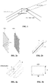
- FIG. 1 When light at an angle of ⁇ is incident in an equivalent optical waveguide unit in the related art, a schematic diagram of a loss region is illustrated in FIG. 1 , where b0' represents a size of the loss region.
- the equivalent optical waveguide unit in the related art is more sensitive to light incident at different angles. As the angle changes, the loss region of the optical waveguide to light becomes larger, resulting in serious the loss of light energy, and part of the lost light may cover an image surface to from ghost light, to affect the viewing effect.
- light intensities at various viewing angles formed by focusing light through a flat lens in the related art are uneven, which affects the actual viewing effect.
- the present disclosure aims to at least solve one of the technical problems in the related art.
- the present disclosure provides an optical waveguide unit.
- the present disclosure further provides an optical waveguide array including optical waveguide units.
- the present disclosure also provides a flat lens including optical waveguide arrays.
- An optical waveguide unit includes: at least one group of total reflection layers, each group including at least one type of total reflection layer, and each type of total reflection layer including at least one single total reflection layer; and at least two sub-waveguides, one group being arranged between every two adjacent sub-waveguides.
- the total reflection layer or the group of total reflection layers may be provided between the sub-waveguides, and each type of total reflection layer corresponds to a different incident angle and optical refractive index. Therefore, the light collection efficiency of the overall optical waveguide unit at the specific incident angle may be improved. The light intensity uniformity of the overall viewing angle may be improved.
- a total height H of the optical waveguide unit satisfies 0.1mm ⁇ H ⁇ 5mm along a stacking direction of the group and the sub-waveguide.
- a number of the sub-waveguides is two, and the group provided between the two sub-waveguides includes one type of total reflection layer.
- a number of the sub-waveguides is four, a number of the groups is three, and the groups include: a first type of total reflection layer in middle; and two second types of total reflection layers, a refractive index of the second type of total reflection layer is different from a refractive index of the first type of total reflection layer, and the two second types of total reflection layers are located on both sides of the first type of total reflection layer along a stacking direction of the group and the sub-waveguide.
- a number of the sub-waveguides is three, a number of the groups is two, and refractive indexes of the two groups are the same or different.
- a thickness of each layer in each type of total reflection layer is 0.04 mm ⁇ t ⁇ 0.2 T i .
- both sides of the optical waveguide unit are provided with reflection layer along a stacking direction of the group and the sub-waveguide.
- the optical waveguide unit according to embodiments of the present disclosure may greatly reduce the loss of light energy and improve the energy uniformity at various viewing angles.
- An optical waveguide array includes: a plurality of optical waveguide units according to embodiments of the first aspect of the present disclosure, each optical waveguide unit having a rectangular cross section, and the plurality of optical waveguide units being joined in parallel; an outer contour of the optical waveguide array is rectangular, and an extending direction of the optical waveguide units and at least two sides of the outer contour of the optical waveguide array form an angle of 30 to 60 degrees.
- the extending direction of the optical waveguide units and the at least two sides of the outer contour of the optical waveguide array form an angle of 45 degrees.
- the plurality of optical waveguide units are joined through an adhesive layer, and a thickness of the adhesive layer is more than 0.001 mm.
- a flat lens according to embodiments of a third aspect of the present disclosure includes two transparent substrates, each transparent substrate having two optical surfaces; two optical waveguide arrays according to embodiments of the second aspect of the present disclosure, in which the two optical waveguide arrays are arranged between the two transparent substrates by means of glue, and optical waveguide extending directions of the two optical waveguide arrays are arranged orthogonally.
- an optical surface of each transparent substrate far away from the optical waveguide array is provided with an antireflection film.
- the array structure is formed by adopting the optical waveguides with single-column multi-row and rectangular cross section, so that the two-dimensional (2D) or 3D light source may be directly formed into a real image in the air to realize a real holographic image, and the imaging effect is good while the naked-eye 3D display characteristics may be realized.
- FIGS. 1 to 5 An optical waveguide array according to embodiments of the present disclosure will be described first with reference to FIGS. 1 to 5 .
- an optical waveguide array 1000a and an optical waveguide array 1000b each includes a plurality of optical waveguide units 100.
- Each optical waveguide unit 100 has a rectangular cross section.
- the plurality of optical waveguide units 100 are joined in parallel.
- the outer contour of the optical waveguide array is rectangular, and the extending direction of the optical waveguide units 100 and at least two sides of the outer contour of the optical waveguide array form an angle of 30 to 60 degrees.
- the extending direction of the optical waveguide units 100 and the at least two sides of the outer contour of the optical waveguide array form an angle of 45 degrees.
- the present disclosure is not limited to this, and a large size requirement may be achieved by splicing a plurality of optical waveguide arrays when a large screen is displayed.
- the overall shape of the optical waveguide arrays is set according to application scene requirements.
- the outer contours of the optical waveguide arrays 1000a, 1000b are both rectangular.
- the optical waveguide unit(s) extending between two diagonal corners of the rectangle has the longest length, and the optical waveguide units 100 located at the two opposite corners have the triangular shape and the shortest length.
- the middle optical waveguide units are in a trapezoidal or parallelogram structure, and the lengths of the optical waveguides are unequal.
- the optical waveguide unit(s) extending between two diagonal corners of the rectangle may be used as a reference, the optical waveguide units on both sides of the optical waveguide unit(s) extending between two diagonal corners of the rectangle may be symmetrically arranged.
- Optical waveguide extending directions of the two optical waveguide arrays 1000a, 1000b are orthogonally arranged to form an equivalent flat lens with a negative refractive index.
- An extending direction of each optical waveguide in the optical waveguide array 1000a is also orthogonal to an extending direction of each optical waveguide in the optical waveguide array 1000b.
- FIG. 4 is a schematic diagram of a principle for modulating light in an overlapping region when two optical waveguide units are placed orthogonally according to embodiments of the present disclosure, in which a and b denote two optical waveguide units, A, B denote odd-order reflected light beams, C denotes transmitted stray light, D denotes an imaging light beam, O denotes an object-side light source point, and Ox denotes an image-side imaging point. Therefore, when the two optical waveguide units are orthogonally placed, the object-side light beam and the image-side light beam are mirror-symmetric with respect to the equivalent flat lens with the negative refractive index, and a negative refraction phenomenon index occurs, thereby realizing imaging of the flat lens, as illustrated in FIG. 5 .
- the plurality of optical waveguide units 100 are joined through an adhesive layer 4, and a thickness of the adhesive layer 4 is more than 0.001 mm.
- the adhesive layer 4 is, for example, a photosensitive adhesive or a heat-sensitive adhesive.
- optical waveguide unit according to embodiments of the present disclosure is described below with reference to FIG. 1 to 10 .
- the optical waveguide unit 100 includes: at least one group 1 of total reflection layers and at least two sub-waveguides 2. One group 1 is arranged between every two adjacent sub-waveguides 2. Each group 1 includes at least one type 11 of total reflection layer. Each type of total reflection layer corresponds to an incident angle and has a different optical refractive index. Each type 11 of total reflection layer includes at least one single total reflection layer. The single total reflection layer in each type has the same optical refractive index.
- the total reflection layer 11 or the group 1 of total reflection layers may be provided between the sub-waveguides 2, and each type of total reflection layer corresponds to a different incident angle and optical refractive index. Therefore, the light collection efficiency of the overall optical waveguide unit 11 at the specific incident angle may be improved. The light intensity uniformity of the overall viewing angle may be improved.
- the material of the total reflection layer used in the optical waveguide unit 100 includes optical glue, optical plastic, optical glass, and the like.
- optical waveguide unit 100 The specific principle of the optical waveguide unit 100 according to the embodiments of the present disclosure will be described below.
- the incident light from the object-side light source point O is reflected inside the equivalent optical waveguide unit and divided into four beams.
- one beam participates in imaging, and the three beams form interference stray light, namely A, B and C.
- the two optical waveguide arrays are arranged at 45° and orthogonal to each other.
- each optical waveguide unit it is easy for each optical waveguide unit to generate stray light, and the stray light is part of the original object light, but may not participate in imaging, which is loss light.
- FIG. 1 when a light beam is incident on the optical waveguide array in the related art at a certain incident angle, there is a loss region with a size b0'. Since the object-side light source is a large-divergence angle light source, the incident angle changes continuously with the light emission of different light sources. The smaller the angle, the larger the loss region and the more serious the light loss, which greatly reduces the light energy utilization rate of the flat lens formed by the optical waveguide array. In addition, different incident angles lead to different energy losses, causing uneven energy in various viewing angles, and affecting the effect of observers observing objects under different viewing angles.
- a plurality of sub-waveguides 2 and a group 1 of total reflection layers or a total reflection layer 11 between the sub-waveguides 2 are arranged in the optical waveguide unit according to embodiments of the present disclosure. Therefore, the light energy located in the loss region b0 may be collected after differentiation of the total reflection layer and the sub-waveguides, and the loss region b0 of light incident from the angle ⁇ may be relatively reduced. As illustrated in FIG. 6
- the function of the total reflection layer 11 is as follows: the light incident on the surface of the optical waveguide unit, which has an angle greater than a critical angle, is totally reflected, and light incident on the surface of the optical waveguide unit, which has an angle smaller than the critical angle, is transmitted.
- the purpose of precise modulation of light near the critical angle may be realized. Therefore, in the disclosure, in order to achieve precise modulation of light near multiple critical angles, it is necessary to provide multiple types 11 of total reflection layers, and the single optical waveguide unit 100 may be divide into multilayer sub-waveguides 1.
- the left side is a normal optical waveguide unit in the related art
- the right side is an optical waveguide unit according to embodiments of the present disclosure.
- FIG. 8 illustrates the comparison on energy uniformity and stray light between the two at various viewing angles. It may be seen that the optical waveguide unit 100 according to embodiments of the present disclosure may greatly reduce the loss of light energy and improve the energy uniformity at various viewing angles.
- a total height H of the optical waveguide unit 100 satisfies 0.1mm ⁇ H ⁇ 5mm along a stacking direction of the group 1 and the sub-waveguide 2.
- a width of a cross section of the optical waveguide unit 100 is W.
- the direction of the width W on the cross section is perpendicular to the stacking direction, that is, the direction of the above-mentioned height H, where W also satisfies 0.1mm ⁇ W ⁇ 5mm.
- a number of the sub-waveguides 2 is two, namely sub-waveguides 21 and 22; and a group 1 of total reflection layers arranged between the two sub-waveguides 2 includes one type 11 of total reflection layer.
- the light near one of the critical angles may be precisely modulated.
- FIG. 9 there are four sub-waveguides 221, 222, 223, and 224.
- a number of the groups 1 of total reflection layers is three.
- the groups 1 include a first type 1121 of total reflection layer in middle; and two second types 1122 of total reflection layers.
- a refractive index of the second type 1122 of total reflection layer is different from a refractive index of the first type 1121 of total reflection layer.
- the two second types 1122 of total reflection layers are located on both sides of the first type 11 of total reflection layer along the stacking direction of the total reflection layer 11 and the sub-waveguide 2.
- FIG. 9 there are four sub-waveguides 221, 222, 223, and 224.
- a number of the groups 1 of total reflection layers is three.
- the groups 1 include a first type 1121 of total reflection layer in middle; and two second types 1122 of total reflection layers.
- a refractive index of the second type 1122 of total reflection layer is different from a refractive index of the first type 1121 of total reflection layer.
- a number of the sub-waveguides 2 is three, a number of the groups 1 is two, and refractive indexes of the two groups 1 are the same or different, which may not be illustrated in FIGS.
- the total reflection layers 11 include the first type 1121 of total reflection layer in middle and two second types 1122 of total reflection layers.
- T1 is the shortest distance that the first type 11 of total reflection layer appears
- T2 is the shortest distance that the second type 11 of total reflection layer appears.
- a thickness of each layer in each type of total reflection layer is 0.04 mm ⁇ t ⁇ 0.2 T i .
- each type of total reflection layer corresponds to ⁇ i and n ei .
- ⁇ i is a selected angle within the viewing angle range, aiming to improve the light collection efficiency of the corresponding angle and increase the uniformity of light intensity in the overall viewing angle.
- the relevant personnel may appropriately increase or decrease the number of total reflection layers and the number of sub-waveguides to the optical waveguide unit 10 to satisfy the light collection requirements during the implementation process.
- the relevant personnel may appropriately increase or decrease the number of total reflection layers and the number of sub-waveguides to the optical waveguide unit 10 to satisfy the light collection requirements during the implementation process.
- multiple types of total reflection layers are required.
- the embodiments of the present disclosure may not impose any restrictions on the number of types and layers of the total reflection layers.
- both sides of the optical waveguide unit 100 are provided with reflection layers 3 along a stacking direction of the group 1 and the sub-waveguide 2, as illustrated in FIG. 9 and FIG. 10 .
- the reflection layer 3 herein uses an aluminum film, which may further reduce the light loss to a certain extent.
- a flat lens according to embodiments of the third aspect of the present disclosure described below with reference to FIG. 11 includes two transparent substrates 2000 and two optical waveguide arrays 1000a, 1000b according to the above embodiments.
- Each of the transparent substrates 2000 has two optical surfaces, and the optical surfaces are used to protect the optical waveguide arrays 1000a, 1000b.
- the two optical waveguide arrays are arranged between the two transparent substrates 2000 by means of glue, and optical waveguide extending directions of the two optical waveguide arrays are arranged orthogonally.
- the extending directions of the optical waveguide units are mutually perpendicular, so that light beams are converged at one point, the object image surface is ensured to be symmetrical relative to the equivalent flat lens with a negative refractive index. Therefore, a negative-refractive-index phenomenon is generated, and imaging of the flat lens is realized.
- the optical waveguide array and the transparent substrate 2000 are also bonded by a photosensitive adhesive or a heat-sensitive adhesive.
- each transparent substrate 200 far away from the optical waveguide array is provided with an antireflection film 210 to further improve the imaging effect.
- the array structure is formed by adopting the optical waveguides with single-column multi-row and rectangular cross section, so that the 2D or 3D light source may be directly formed into a real image in the air to realize a real holographic image, and the imaging effect is good while the naked-eye 3D display characteristics may be realized.
Landscapes
- Physics & Mathematics (AREA)
- General Physics & Mathematics (AREA)
- Optics & Photonics (AREA)
- Optical Couplings Of Light Guides (AREA)
- Optical Elements Other Than Lenses (AREA)
- Optical Integrated Circuits (AREA)
Applications Claiming Priority (1)
| Application Number | Priority Date | Filing Date | Title |
|---|---|---|---|
| PCT/CN2019/087108 WO2020227993A1 (zh) | 2019-05-15 | 2019-05-15 | 光波导单元、阵列及平板透镜 |
Publications (4)
| Publication Number | Publication Date |
|---|---|
| EP3933465A1 true EP3933465A1 (de) | 2022-01-05 |
| EP3933465A4 EP3933465A4 (de) | 2022-03-09 |
| EP3933465B1 EP3933465B1 (de) | 2023-09-06 |
| EP3933465C0 EP3933465C0 (de) | 2023-09-06 |
Family
ID=73290122
Family Applications (1)
| Application Number | Title | Priority Date | Filing Date |
|---|---|---|---|
| EP19928498.5A Active EP3933465B1 (de) | 2019-05-15 | 2019-05-15 | Optische wellenleitereinheit und anordnung sowie flache linse |
Country Status (6)
| Country | Link |
|---|---|
| US (2) | US12399365B2 (de) |
| EP (1) | EP3933465B1 (de) |
| JP (2) | JP7345555B2 (de) |
| KR (2) | KR102747053B1 (de) |
| SG (1) | SG11202111359PA (de) |
| WO (1) | WO2020227993A1 (de) |
Cited By (1)
| Publication number | Priority date | Publication date | Assignee | Title |
|---|---|---|---|---|
| EP3926373A4 (de) * | 2019-06-26 | 2022-02-23 | Anhui Easpeed Technology Co., Ltd. | Optische wellenleitereinheit, optisches wellenleiterarray und flache linse |
Families Citing this family (2)
| Publication number | Priority date | Publication date | Assignee | Title |
|---|---|---|---|---|
| CN113436560B (zh) * | 2021-06-09 | 2022-11-18 | 安徽省东超科技有限公司 | 成像光学系统及显示装置 |
| CN114637127A (zh) * | 2022-02-24 | 2022-06-17 | 安徽省东超科技有限公司 | 应用于光学成像系统的视场控制装置以及光学成像系统 |
Family Cites Families (16)
| Publication number | Priority date | Publication date | Assignee | Title |
|---|---|---|---|---|
| US6485145B1 (en) * | 1999-12-21 | 2002-11-26 | Scram Technologies, Inc. | Optical system for display panel |
| JP2004287181A (ja) * | 2003-03-24 | 2004-10-14 | Toyoda Mach Works Ltd | 光導波路、光導波路アレイ及びレーザ集光装置 |
| JP5921243B2 (ja) * | 2012-02-14 | 2016-05-24 | シャープ株式会社 | 反射型結像素子および光学システム |
| US20150212335A1 (en) | 2012-08-03 | 2015-07-30 | Sharp Kabushiki Kaisha | Reflective type imaging element and optical system, and method of manufacturing relective type imaging element |
| US9864178B2 (en) | 2013-04-12 | 2018-01-09 | Sharp Kabushiki Kaisha | Reflection imaging device and method of producing reflection imaging device |
| JP2016180785A (ja) | 2015-03-23 | 2016-10-13 | コニカミノルタ株式会社 | 反射型空中結像素子及びその製造方法 |
| JP2016224110A (ja) * | 2015-05-27 | 2016-12-28 | シャープ株式会社 | 光学結合素子 |
| JP6165206B2 (ja) | 2015-09-08 | 2017-07-19 | 松浪硝子工業株式会社 | 光制御パネルの製造方法、光制御パネル、光学結像装置、及び、空中映像形成システム |
| US11231544B2 (en) * | 2015-11-06 | 2022-01-25 | Magic Leap, Inc. | Metasurfaces for redirecting light and methods for fabricating |
| JP2017181854A (ja) | 2016-03-31 | 2017-10-05 | コニカミノルタ株式会社 | 結像素子の製造方法 |
| WO2017175671A1 (ja) | 2016-04-07 | 2017-10-12 | コニカミノルタ株式会社 | 結像素子 |
| TW201805661A (zh) | 2016-08-15 | 2018-02-16 | 鴻海精密工業股份有限公司 | 能夠在空氣中顯示影像的顯示器及成像系統 |
| JP6574910B2 (ja) | 2016-12-06 | 2019-09-11 | コニカミノルタ株式会社 | 反射型空中結像素子 |
| CN107340567A (zh) * | 2017-09-01 | 2017-11-10 | 上海誉沛光电科技有限公司 | 一种平板光波导和显示装置 |
| CN107807417A (zh) * | 2017-12-09 | 2018-03-16 | 安徽省东超科技有限公司 | 单列多排等效负折射率平板透镜 |
| CN109917513B (zh) * | 2019-05-15 | 2019-09-20 | 上海先研光电科技有限公司 | 一种光波导及应用光波导的平板透镜 |
-
2019
- 2019-05-15 KR KR1020217031514A patent/KR102747053B1/ko active Active
- 2019-05-15 JP JP2021549535A patent/JP7345555B2/ja active Active
- 2019-05-15 EP EP19928498.5A patent/EP3933465B1/de active Active
- 2019-05-15 WO PCT/CN2019/087108 patent/WO2020227993A1/zh not_active Ceased
- 2019-05-15 SG SG11202111359PA patent/SG11202111359PA/en unknown
- 2019-05-15 KR KR1020247042435A patent/KR20250002846A/ko active Pending
-
2021
- 2021-10-15 US US17/451,077 patent/US12399365B2/en active Active
-
2023
- 2023-09-05 JP JP2023143921A patent/JP7659602B2/ja active Active
-
2025
- 2025-07-15 US US19/269,668 patent/US20250347918A1/en active Pending
Cited By (2)
| Publication number | Priority date | Publication date | Assignee | Title |
|---|---|---|---|---|
| EP3926373A4 (de) * | 2019-06-26 | 2022-02-23 | Anhui Easpeed Technology Co., Ltd. | Optische wellenleitereinheit, optisches wellenleiterarray und flache linse |
| US11977245B2 (en) | 2019-06-26 | 2024-05-07 | Anhui Easpeed Technology Co., Ltd. | Optical waveguide unit, array, and flat lens |
Also Published As
| Publication number | Publication date |
|---|---|
| SG11202111359PA (en) | 2021-11-29 |
| JP7659602B2 (ja) | 2025-04-09 |
| US12399365B2 (en) | 2025-08-26 |
| JP2022521424A (ja) | 2022-04-07 |
| KR20210134364A (ko) | 2021-11-09 |
| EP3933465B1 (de) | 2023-09-06 |
| KR102747053B1 (ko) | 2024-12-24 |
| JP2023178517A (ja) | 2023-12-15 |
| EP3933465C0 (de) | 2023-09-06 |
| US20250347918A1 (en) | 2025-11-13 |
| US20220035094A1 (en) | 2022-02-03 |
| EP3933465A4 (de) | 2022-03-09 |
| WO2020227993A1 (zh) | 2020-11-19 |
| KR20250002846A (ko) | 2025-01-07 |
| JP7345555B2 (ja) | 2023-09-15 |
Similar Documents
| Publication | Publication Date | Title |
|---|---|---|
| US20250347918A1 (en) | Optical waveguide unit, array, and flat lens | |
| US11909949B2 (en) | Display panel, display method thereof and display device | |
| US10330938B2 (en) | Waveguide optical element and near-eye display apparatus | |
| WO2022147866A1 (zh) | 一种大视场角的光学扩瞳装置、显示装置及方法 | |
| CN110908134A (zh) | 一种显示装置及显示系统 | |
| WO2019109585A1 (zh) | 多排多列等效负折射率平板透镜 | |
| CN111856851A (zh) | 一种复合微透镜和微棱镜的投影系统 | |
| US11966049B2 (en) | Pupil tracking near-eye display | |
| CN104423050A (zh) | 裸眼立体显示装置 | |
| US20190317266A1 (en) | Display device | |
| CN110286494B (zh) | 光波导单元、阵列及平板透镜 | |
| US11982838B2 (en) | Optical lens | |
| CN210181311U (zh) | 光波导单元、阵列及平板透镜 | |
| CN116149077A (zh) | 用于悬浮图像的拼接显示装置以及包括其的多层显示设备 | |
| WO2022226829A1 (zh) | 一种光场显示装置及其显示方法 | |
| CN210005808U (zh) | 光波导单元、阵列及平板透镜 | |
| CN110262047B (zh) | 光波导单元、阵列及平板透镜 | |
| CN211905753U (zh) | 一种光学透镜 | |
| CN211905883U (zh) | 一种多视点空中成像装置 | |
| US11977245B2 (en) | Optical waveguide unit, array, and flat lens | |
| CN211905884U (zh) | 一种360度空中成像装置 | |
| US12537931B2 (en) | Display apparatus including an imaging structure comprising light-shielding layer and method for maufacturing same | |
| CN211905758U (zh) | 一种光波导成像透镜 | |
| CN115079416B (zh) | 扩增实境眼镜 |
Legal Events
| Date | Code | Title | Description |
|---|---|---|---|
| STAA | Information on the status of an ep patent application or granted ep patent |
Free format text: STATUS: THE INTERNATIONAL PUBLICATION HAS BEEN MADE |
|
| PUAI | Public reference made under article 153(3) epc to a published international application that has entered the european phase |
Free format text: ORIGINAL CODE: 0009012 |
|
| STAA | Information on the status of an ep patent application or granted ep patent |
Free format text: STATUS: REQUEST FOR EXAMINATION WAS MADE |
|
| 17P | Request for examination filed |
Effective date: 20210915 |
|
| AK | Designated contracting states |
Kind code of ref document: A1 Designated state(s): AL AT BE BG CH CY CZ DE DK EE ES FI FR GB GR HR HU IE IS IT LI LT LU LV MC MK MT NL NO PL PT RO RS SE SI SK SM TR |
|
| A4 | Supplementary search report drawn up and despatched |
Effective date: 20220207 |
|
| RIC1 | Information provided on ipc code assigned before grant |
Ipc: G02B 30/56 20200101ALI20220201BHEP Ipc: G02B 17/00 20060101ALI20220201BHEP Ipc: G02B 6/00 20060101AFI20220201BHEP |
|
| DAV | Request for validation of the european patent (deleted) | ||
| DAX | Request for extension of the european patent (deleted) | ||
| STAA | Information on the status of an ep patent application or granted ep patent |
Free format text: STATUS: EXAMINATION IS IN PROGRESS |
|
| 17Q | First examination report despatched |
Effective date: 20220913 |
|
| REG | Reference to a national code |
Ref legal event code: R079 Free format text: PREVIOUS MAIN CLASS: G02B0006000000 Ref country code: DE Ref legal event code: R079 Ref document number: 602019037167 Country of ref document: DE Free format text: PREVIOUS MAIN CLASS: G02B0006000000 Ipc: F21V0008000000 |
|
| GRAP | Despatch of communication of intention to grant a patent |
Free format text: ORIGINAL CODE: EPIDOSNIGR1 |
|
| STAA | Information on the status of an ep patent application or granted ep patent |
Free format text: STATUS: GRANT OF PATENT IS INTENDED |
|
| RIC1 | Information provided on ipc code assigned before grant |
Ipc: G02B 30/56 20200101ALI20230314BHEP Ipc: G02B 17/00 20060101ALI20230314BHEP Ipc: F21V 8/00 20060101AFI20230314BHEP |
|
| INTG | Intention to grant announced |
Effective date: 20230413 |
|
| GRAS | Grant fee paid |
Free format text: ORIGINAL CODE: EPIDOSNIGR3 |
|
| GRAA | (expected) grant |
Free format text: ORIGINAL CODE: 0009210 |
|
| STAA | Information on the status of an ep patent application or granted ep patent |
Free format text: STATUS: THE PATENT HAS BEEN GRANTED |
|
| AK | Designated contracting states |
Kind code of ref document: B1 Designated state(s): AL AT BE BG CH CY CZ DE DK EE ES FI FR GB GR HR HU IE IS IT LI LT LU LV MC MK MT NL NO PL PT RO RS SE SI SK SM TR |
|
| REG | Reference to a national code |
Ref country code: GB Ref legal event code: FG4D |
|
| REG | Reference to a national code |
Ref country code: CH Ref legal event code: EP |
|
| REG | Reference to a national code |
Ref country code: IE Ref legal event code: FG4D |
|
| REG | Reference to a national code |
Ref country code: DE Ref legal event code: R096 Ref document number: 602019037167 Country of ref document: DE |
|
| U01 | Request for unitary effect filed |
Effective date: 20230926 |
|
| U07 | Unitary effect registered |
Designated state(s): AT BE BG DE DK EE FI FR IT LT LU LV MT NL PT SE SI Effective date: 20231004 |
|
| PG25 | Lapsed in a contracting state [announced via postgrant information from national office to epo] |
Ref country code: GR Free format text: LAPSE BECAUSE OF FAILURE TO SUBMIT A TRANSLATION OF THE DESCRIPTION OR TO PAY THE FEE WITHIN THE PRESCRIBED TIME-LIMIT Effective date: 20231207 |
|
| PG25 | Lapsed in a contracting state [announced via postgrant information from national office to epo] |
Ref country code: RS Free format text: LAPSE BECAUSE OF FAILURE TO SUBMIT A TRANSLATION OF THE DESCRIPTION OR TO PAY THE FEE WITHIN THE PRESCRIBED TIME-LIMIT Effective date: 20230906 Ref country code: NO Free format text: LAPSE BECAUSE OF FAILURE TO SUBMIT A TRANSLATION OF THE DESCRIPTION OR TO PAY THE FEE WITHIN THE PRESCRIBED TIME-LIMIT Effective date: 20231206 Ref country code: HR Free format text: LAPSE BECAUSE OF FAILURE TO SUBMIT A TRANSLATION OF THE DESCRIPTION OR TO PAY THE FEE WITHIN THE PRESCRIBED TIME-LIMIT Effective date: 20230906 Ref country code: GR Free format text: LAPSE BECAUSE OF FAILURE TO SUBMIT A TRANSLATION OF THE DESCRIPTION OR TO PAY THE FEE WITHIN THE PRESCRIBED TIME-LIMIT Effective date: 20231207 |
|
| PG25 | Lapsed in a contracting state [announced via postgrant information from national office to epo] |
Ref country code: IS Free format text: LAPSE BECAUSE OF FAILURE TO SUBMIT A TRANSLATION OF THE DESCRIPTION OR TO PAY THE FEE WITHIN THE PRESCRIBED TIME-LIMIT Effective date: 20240106 |
|
| PG25 | Lapsed in a contracting state [announced via postgrant information from national office to epo] |
Ref country code: ES Free format text: LAPSE BECAUSE OF FAILURE TO SUBMIT A TRANSLATION OF THE DESCRIPTION OR TO PAY THE FEE WITHIN THE PRESCRIBED TIME-LIMIT Effective date: 20230906 |
|
| PG25 | Lapsed in a contracting state [announced via postgrant information from national office to epo] |
Ref country code: SM Free format text: LAPSE BECAUSE OF FAILURE TO SUBMIT A TRANSLATION OF THE DESCRIPTION OR TO PAY THE FEE WITHIN THE PRESCRIBED TIME-LIMIT Effective date: 20230906 Ref country code: RO Free format text: LAPSE BECAUSE OF FAILURE TO SUBMIT A TRANSLATION OF THE DESCRIPTION OR TO PAY THE FEE WITHIN THE PRESCRIBED TIME-LIMIT Effective date: 20230906 Ref country code: IS Free format text: LAPSE BECAUSE OF FAILURE TO SUBMIT A TRANSLATION OF THE DESCRIPTION OR TO PAY THE FEE WITHIN THE PRESCRIBED TIME-LIMIT Effective date: 20240106 Ref country code: ES Free format text: LAPSE BECAUSE OF FAILURE TO SUBMIT A TRANSLATION OF THE DESCRIPTION OR TO PAY THE FEE WITHIN THE PRESCRIBED TIME-LIMIT Effective date: 20230906 Ref country code: CZ Free format text: LAPSE BECAUSE OF FAILURE TO SUBMIT A TRANSLATION OF THE DESCRIPTION OR TO PAY THE FEE WITHIN THE PRESCRIBED TIME-LIMIT Effective date: 20230906 Ref country code: SK Free format text: LAPSE BECAUSE OF FAILURE TO SUBMIT A TRANSLATION OF THE DESCRIPTION OR TO PAY THE FEE WITHIN THE PRESCRIBED TIME-LIMIT Effective date: 20230906 |
|
| U20 | Renewal fee for the european patent with unitary effect paid |
Year of fee payment: 6 Effective date: 20240425 |
|
| PG25 | Lapsed in a contracting state [announced via postgrant information from national office to epo] |
Ref country code: PL Free format text: LAPSE BECAUSE OF FAILURE TO SUBMIT A TRANSLATION OF THE DESCRIPTION OR TO PAY THE FEE WITHIN THE PRESCRIBED TIME-LIMIT Effective date: 20230906 |
|
| REG | Reference to a national code |
Ref country code: DE Ref legal event code: R097 Ref document number: 602019037167 Country of ref document: DE |
|
| PLBE | No opposition filed within time limit |
Free format text: ORIGINAL CODE: 0009261 |
|
| STAA | Information on the status of an ep patent application or granted ep patent |
Free format text: STATUS: NO OPPOSITION FILED WITHIN TIME LIMIT |
|
| 26N | No opposition filed |
Effective date: 20240607 |
|
| U1N | Appointed representative for the unitary patent procedure changed after the registration of the unitary effect |
Representative=s name: KARO IP; DE |
|
| REG | Reference to a national code |
Ref country code: CH Ref legal event code: PL |
|
| PG25 | Lapsed in a contracting state [announced via postgrant information from national office to epo] |
Ref country code: MC Free format text: LAPSE BECAUSE OF FAILURE TO SUBMIT A TRANSLATION OF THE DESCRIPTION OR TO PAY THE FEE WITHIN THE PRESCRIBED TIME-LIMIT Effective date: 20230906 |
|
| PG25 | Lapsed in a contracting state [announced via postgrant information from national office to epo] |
Ref country code: MC Free format text: LAPSE BECAUSE OF FAILURE TO SUBMIT A TRANSLATION OF THE DESCRIPTION OR TO PAY THE FEE WITHIN THE PRESCRIBED TIME-LIMIT Effective date: 20230906 Ref country code: CH Free format text: LAPSE BECAUSE OF NON-PAYMENT OF DUE FEES Effective date: 20240531 |
|
| PG25 | Lapsed in a contracting state [announced via postgrant information from national office to epo] |
Ref country code: IE Free format text: LAPSE BECAUSE OF NON-PAYMENT OF DUE FEES Effective date: 20240515 |
|
| U20 | Renewal fee for the european patent with unitary effect paid |
Year of fee payment: 7 Effective date: 20250425 |
|
| PGFP | Annual fee paid to national office [announced via postgrant information from national office to epo] |
Ref country code: GB Payment date: 20250521 Year of fee payment: 7 |
|
| PG25 | Lapsed in a contracting state [announced via postgrant information from national office to epo] |
Ref country code: CY Free format text: LAPSE BECAUSE OF FAILURE TO SUBMIT A TRANSLATION OF THE DESCRIPTION OR TO PAY THE FEE WITHIN THE PRESCRIBED TIME-LIMIT; INVALID AB INITIO Effective date: 20190515 |
|
| PG25 | Lapsed in a contracting state [announced via postgrant information from national office to epo] |
Ref country code: HU Free format text: LAPSE BECAUSE OF FAILURE TO SUBMIT A TRANSLATION OF THE DESCRIPTION OR TO PAY THE FEE WITHIN THE PRESCRIBED TIME-LIMIT; INVALID AB INITIO Effective date: 20190515 |