EP3933483A1 - Optischer scanner - Google Patents
Optischer scanner Download PDFInfo
- Publication number
- EP3933483A1 EP3933483A1 EP21179932.5A EP21179932A EP3933483A1 EP 3933483 A1 EP3933483 A1 EP 3933483A1 EP 21179932 A EP21179932 A EP 21179932A EP 3933483 A1 EP3933483 A1 EP 3933483A1
- Authority
- EP
- European Patent Office
- Prior art keywords
- optical
- layer
- scanner
- face
- beams
- Prior art date
- Legal status (The legal status is an assumption and is not a legal conclusion. Google has not performed a legal analysis and makes no representation as to the accuracy of the status listed.)
- Granted
Links
Images




Classifications
-
- G—PHYSICS
- G02—OPTICS
- G02B—OPTICAL ELEMENTS, SYSTEMS OR APPARATUS
- G02B26/00—Optical devices or arrangements for the control of light using movable or deformable optical elements
- G02B26/06—Optical devices or arrangements for the control of light using movable or deformable optical elements for controlling the phase of light
-
- G—PHYSICS
- G02—OPTICS
- G02B—OPTICAL ELEMENTS, SYSTEMS OR APPARATUS
- G02B6/00—Light guides; Structural details of arrangements comprising light guides and other optical elements, e.g. couplings
- G02B6/24—Coupling light guides
- G02B6/26—Optical coupling means
- G02B6/28—Optical coupling means having data bus means, i.e. plural waveguides interconnected and providing an inherently bidirectional system by mixing and splitting signals
- G02B6/293—Optical coupling means having data bus means, i.e. plural waveguides interconnected and providing an inherently bidirectional system by mixing and splitting signals with wavelength selective means
- G02B6/29301—Optical coupling means having data bus means, i.e. plural waveguides interconnected and providing an inherently bidirectional system by mixing and splitting signals with wavelength selective means based on a phased array of light guides
-
- G—PHYSICS
- G02—OPTICS
- G02B—OPTICAL ELEMENTS, SYSTEMS OR APPARATUS
- G02B26/00—Optical devices or arrangements for the control of light using movable or deformable optical elements
- G02B26/08—Optical devices or arrangements for the control of light using movable or deformable optical elements for controlling the direction of light
- G02B26/10—Scanning systems
- G02B26/101—Scanning systems with both horizontal and vertical deflecting means, e.g. raster or XY scanners
-
- G—PHYSICS
- G02—OPTICS
- G02B—OPTICAL ELEMENTS, SYSTEMS OR APPARATUS
- G02B26/00—Optical devices or arrangements for the control of light using movable or deformable optical elements
- G02B26/08—Optical devices or arrangements for the control of light using movable or deformable optical elements for controlling the direction of light
- G02B26/10—Scanning systems
- G02B26/103—Scanning systems having movable or deformable optical fibres, light guides or waveguides as scanning elements
-
- G—PHYSICS
- G02—OPTICS
- G02B—OPTICAL ELEMENTS, SYSTEMS OR APPARATUS
- G02B26/00—Optical devices or arrangements for the control of light using movable or deformable optical elements
- G02B26/08—Optical devices or arrangements for the control of light using movable or deformable optical elements for controlling the direction of light
- G02B26/10—Scanning systems
- G02B26/106—Scanning systems having diffraction gratings as scanning elements, e.g. holographic scanners
-
- G—PHYSICS
- G02—OPTICS
- G02B—OPTICAL ELEMENTS, SYSTEMS OR APPARATUS
- G02B27/00—Optical systems or apparatus not provided for by any of the groups G02B1/00 - G02B26/00, G02B30/00
- G02B27/0087—Phased arrays
Definitions
- the present invention relates to the field of opto-electromechanical microsystems (“MOEMS” according to Anglo-Saxon terminology).
- the present invention relates to an optical scanner provided with a plurality of elementary scanners arranged to scan the space surrounding the optical scanner by means of a plurality of light beams.
- each elementary scanner according to the present invention combines a beam provided with a movable part to which bending can be imposed, and a phase-controlled network.
- at least one beam among the set of beams of the elementary scanners has an arrow different from that of the other beams so as to extend the surface capable of being scanned by all of the light beams extracted from the scanner.
- 2D scanners or micro-scanners are devices allowing a scene to be swept with a light beam in one or even two dimensions. These scanners can in particular be used in devices of the LIDAR (“Light Detection And Ranging systems”) type for detection or imaging purposes.
- LIDAR Light Detection And Ranging systems
- the scanning of a surface or of an object by a light beam can be carried out by means of one or more mobile micro-mirrors.
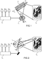
- the figure 1 (extracted from the document [1] cited at the end of the description) illustrates a first possible architecture of such a device provided with two micro-mirrors, respectively called the first micro-mirror 1 1 and second micro-mirror 2 1 , arranged for pivot around, respectively, a first pivot axis X 1 X 1 'and a second pivot axis Y 1 Y 1 ' which are not parallel.
- these two micro-mirrors 1 1 and 2 1 are arranged so that a light beam emitted by a light source 3 1 is reflected by the first micro-mirror 1 1 in the direction of the second micro-mirror 2 1 which it reflects in turn in the direction of, for example, a screen 4 1 .
- the rotation of each of the micro-mirrors 1 1 and 2 1 around their respective pivot axis thus makes it possible to perform a scanning a surface with the light beam, for example for imaging or detection purposes.
- micro-mirrors are also liable to be damaged, in particular by heating induced by the light beam.
- a second architecture illustrated on figure 2 (extracted from document [1] cited at the end of the description), can be considered.
- the latter uses a single micro-mirror 1 2 mounted to pivot about two pivot axes X 2 X 2 'and Y 2 Y 2 ' which are not parallel.
- the oscillation of this micro-mirror 1 2 around one and the other of the two pivot axes X 2 X 2 'and Y 2 Y 2 ' thus makes it possible to scan the surface of a screen 4 1 by means of a light beam from a light source 3 2 and reflected by said micromirror 1 2 .
- the micro-mirror 1 2 is also likely to undergo heating induced by the light beam.
- this second architecture is also sensitive to the alignment of the light source 3 2 and of the micro-mirror 1 2 .
- the alignment between these two elements is particularly sensitive to the shocks undergone by the device but also to the temperature and pressure conditions imposed on the latter.
- 2D micro-scanners with phase-controlled optical emitter or with optical grating with phase control (“OPA” or “Optical Phased Array” according to Anglo-Saxon terminology) could be proposed.
- the latter may comprise a plurality of optical sources each capable of emitting light radiation.
- Each of its optical sources is also associated with phase modulation means intended to phase shift the optical radiations with respect to each other so as to vary the propagation angle of the combined radiation coming from all of the optical sources.
- the optical sources can come from the same main source.
- This operating principle can be extrapolated to a 2D matrix of optical sources allowing scanning of an optical beam in two different directions, for example perpendicular to one another.
- an aim of the present invention is to provide a light scanning device which makes it possible to scan a larger space than the devices known from the state of the art.
- Another object of the present invention is to provide a light scanning device which has appreciable compactness.
- Another object of the present invention is to provide a light scanning device that is simpler to manufacture.
- the movable part of at least one of the beams has, at rest, an arrow different from the arrows at rest of the movable parts of the other beams.
- the movable parts of each of the beams all have, at rest, a different deflection.
- each beam comprises from a first face towards a second face parallel to the first face, a first layer, a second layer and a third layer, the deflection of the mobile part of each of the beams being imposed.
- an internal stress level of one and / or the other of the first layer and of the third layer advantageously the stress level of one and / or the other of the first layer and of the third layer is a function of the thickness of the layer concerned.
- the first layer and the third layer each comprise a dielectric material, advantageously, the dielectric material comprises silicon dioxide.
- each optical phase shifter comprises a diffraction grating coupled to phase shift means intended to impose a phase shift on the secondary optical beam coming from the waveguide to which the optical phase shifter in question is optically coupled.
- the waveguides and / or the diffraction gratings comprise silicon nitride.
- the optical phase shifters are arranged in lines parallel or perpendicular to an axis of elongation XX 'defined by the fixed end and the free end.
- the optical phase shifters are arranged in a matrix manner.
- each elementary scanner is also provided with an actuator arranged to impose bending on the mobile part of the beam in question.
- the actuator comprises at least one of the means chosen from: electrostatic means, magnetic means, piezoelectric means, thermal means.
- the invention is not however limited to these means alone.
- the support is of parallelepipedal or cylindrical or other shape.
- the invention is not limited to these shapes alone.
- the support can take other regular or irregular shapes, for example pyramidal.
- the present invention relates to a scanner provided with a plurality of elementary scanners each capable of scanning a different surface by means of a light beam.
- each elementary scanner comprises a beam, for example a vibrating beam, on or in which is formed a phase-controlled network intended to extract a light beam at the level of one face of the beam. capable of being emitted by a light source.
- at least one beam of one of the elementary scanners called the first scanner, has, at rest, an arrow different from that of the beams of the other elementary scanners. This arrangement allows the first scanner to scan a surface, called the first surface, different from that scanned by the other elementary scanners.
- the optical scanner according to the present invention makes it possible to cover a relatively large area while maintaining appreciable compactness.
- FIG. 3a and 3b are schematic representations of an exemplary implementation of a scanner 10 according to the present invention.
- the scanner 10 comprises in particular a fixed support 20 provided with a main face 21.
- the support 20 can in particular be obtained from a semiconductor substrate, for example silicon.
- said support 20 can comprise any other material capable of performing the support function.
- the support 20 can be of parallelepipedal or cylindrical shape, without however limiting the invention to these shapes only ( figures 10a and 10b ).
- the scanner 10 also comprises at least one optical source, for example a single source 50, capable of emitting a main optical beam of a wavelength ⁇ ( figure 4 ).
- at least one optical source for example a single source 50, capable of emitting a main optical beam of a wavelength ⁇ ( figure 4 ).
- the main optical beam is advantageously quasi-monochromatic, or even monochromatic.
- the optical source 50 can for example comprise a LASER source.
- the wavelength ⁇ can be between 400 nm and 2500 nm, for example be equal to 905 nm, or equal to 1330 nm or even equal to 1550 nm.
- the scanner 10 also comprises a plurality of elementary scanners 11, for example three in number on the figures 3a and 3b .
- an elementary scanner 11 comprises a beam 30 provided with a first face 31 and a second face 32, and which extends along an axis of elongation XX 'from a fixed end 33 to a free end 34.
- beam is understood to mean a solid mechanical element of generally elongated shape.
- a beam according to the terms of the present invention can be of parallelepiped shape.
- axis of elongation XX ' within the meaning of the present invention, is not necessarily linear and can consequently have a curvature (and therefore an arrow). This aspect is described in more detail in the remainder of the present description.
- the beam 30 also comprises a movable part 36 which extends from the free end 34 towards the fixed end 33.
- the beam 30 can also include a fixed part 35, in the extension of the movable part and in the direction of the fixed end 33.
- the beam 30 is in particular secured to the support 20 by its fixed part 35.
- the fixed part 35 rests on the main face 21.
- the term “mobile part” is understood to mean a part of a beam capable of undergoing deformation by bending and / or by torsion.
- the movable part can undergo a bending in a direction perpendicular to the first face and / or a torsion around an axis of elongation XX 'defined by the fixed end and the free end.
- the beam 30 may have a thickness of between 1 ⁇ m and several hundred ⁇ l, a length of between 100 ⁇ m and several millimeters, and a width of between 10 ⁇ m and several millimeters.
- the thickness of the beam is defined as the distance between the first face and the second face.
- the length of the beam is its dimension measured along the direction defined by the axis of elongation XX 'while its width is its dimension measured in a direction perpendicular to that defined by the axis of elongation XX' and the thickness of said beam.
- Each elementary scanner 11 also comprises a plurality of waveguides 60i arranged on or in the beam 30 and intended to divide the main optical beam into a plurality of secondary optical beams.
- the figure 5 illustrious to In this regard, a possible arrangement of the waveguides 60i in a view directly above the first face 31.
- These waveguides are, according to this example, arranged parallel to the axis of elongation XX ', and so that the ratio between their spacing (in ⁇ m) and the wavelength ⁇ (in nm) is between 0.5 and 10.
- the waveguides can for example be of a length of between a hundred microns and ten millimeters, and be spaced from each other by a distance of between a hundred microns and ten millimeters.
- the main optical beam emitted by the optical source 50 is advantageously transmitted at the level of the beams 30 by optical coupling means 51, for example by one or more optical fibers ( figure 4 ).
- Each elementary scanner 11 also comprises a phase-controlled optical network 70 which comprises a plurality of optical phase shifters.
- the phase-controlled network 70 can be controlled by control means.
- the phase-controlled optical network 70 includes a plurality of optical phase shifters 71i each coupled to a waveguide 60i.
- the optical phase shifters 71i are moreover arranged on or in an emission section 37 of the movable part 36 and which extends from the free end 34.
- each optical phase shifter 70i can comprise a diffraction grating 71i coupled to phase shift means 72i.
- each phase shifting means 72i is intended to impose a phase shift on the secondary optical beam coming from the waveguide 60i to which the considered optical phase shifter 70i is optically coupled.
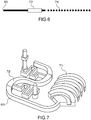
- the figure 6 is an illustration of an optical phase shifter 70i according to a first architecture capable of being implemented within the framework of the present invention.
- the diffraction grating 71i is formed of pads aligned in the extension of the waveguide 60i, while the phase-shifting means 72i may comprise a heating element placed directly above the waveguide 60i and intended to locally heat the latter in order to modulate its refractive index.
- the figure 7 is an illustration of an optical phase shifter 70i according to a second architecture capable of being implemented within the framework of the present invention.
- the diffraction grating 71i is formed of aligned solid arcs, while the phase shifting means 72i can comprise a heating element intended to locally heat the waveguide 60i in order to modulate its refractive index.
- the waveguides and / or the diffraction gratings can comprise silicon nitride.
- the optical phase shifters can be arranged in a line perpendicular to an axis of elongation XX 'defined by the fixed end and the free end ( figure 5 ).
- the main optical beam emitted by the optical source is firstly divided into a plurality of secondary optical beams guided by the plurality of waveguides 60i.
- Each secondary optical beam guided by a given waveguide is then extracted from the beam by means of the diffraction grating 71i with which the considered waveguide is associated.
- the set of secondary optical beams thus extracted from the same beam recombine to form a beam called the elementary beam.
- a phase shift between the optical beams of the same beam induced by the phase shift means 72i makes it possible to vary the angle of propagation of the elementary beam. This propagation angle varies in particular in a plane normal to the first face and which includes the direction of alignment of the optical phase shifters.
- the optical phase shifters 70i can be arranged in lines parallel to the axis of elongation XX '.
- the optical phase shifters 70i can be arranged in a matrix fashion.
- an elementary scanner can thus scan the space according to two propagation angles.
- the movable part of at least one of the beams has, at rest, an arrow different from the arrows at rest of the movable parts of the other beams.
- arrow is meant a deformation or a deflection of the movable part of the beam relative to a rectilinear elongation axis.
- the deflection can be characterized by a deflection angle at rest.
- a deflection at rest corresponds to an intrinsic deformation of the moving part.
- this deformation of the movable part does not result from an external action or from the application of a particular stress at the level of said movable part.
- the deflection at rest of the mobile part depends on the internal stresses of the constituent materials of the beam.
- the documents [2] and [3] cited at the end of the description relate to the effect of such stresses on the deflection at rest of the beam.
- a layer exhibiting a tensile stress (and conversely compression) placed between the neutral fiber of the beam and its second face will cause bending of said beam in a direction normal to said second face (conversely in a direction opposite to the direction normal to the second face).
- a layer having a tensile stress (and conversely compression) placed between the neutral fiber of the beam and its first face will cause a bending of said beam in a direction normal to said first face (conversely in a direction opposite to direction normal to the first face).
- the properties (and in particular their internal stresses and / or their thicknesses) of the constituent layers of the beam thus govern the bending at rest, (as well as its amplitude) of the beam.
- optical scanner 10 The difference in deflection between moving parts allows each elementary scanner to scan, with the elementary beam which is associated with it, a different zone or surface.
- the surface thus covered by the optical scanner 10 according to the present invention is increased with regard to optical scanners known from the state of the art.
- the deflection at rest of the mobile part can result from an internal stress induced by the structure of the beam.
- the beam 30 of an elementary scanner 11 can comprise, from its first face 31 to its second face 32, a first layer, a second layer and a third layer.
- the deflection of the mobile part of each of the beams is imposed by a stress level of one and / or the other of the first layer 30 1 and of the third layer 30 3 .
- the stress level of one and / or the other of the first layer 30 1 and of the third layer 30 3 depends on the thickness of the layer concerned.
- the first layer 30 1 and the third layer 30 3 can advantageously comprise a dielectric material and more particularly silicon dioxide.
- the second layer 30 2 can comprise a semiconductor material, advantageously silicon, and even more advantageously polycrystalline silicon.
- a first layer made of SiO 2 having a compressive stress of the order of 200 MPa and a Young's modulus of 70 GPA will cause bending in a direction normal to the first face. This bending is all the more important as the thickness of said layer is high.
- a third layer made of TEOS exhibiting a compressive stress of the order of 80 MPa and a Young's modulus of 70 GPa will cause bending in a direction normal to the second face. This bending is all the more important as the thickness of said layer is high.
- the consideration according to the present invention of a beam having a deflection at rest that is different from one elementary scanner to another allows each of the latter to scan a different surface, called the elementary surface.
- the elementary surfaces combined with one another then form the total surface capable of being scanned by the optical scanner 10. This total surface can in particular be modulated according to the number of elementary scanners and their arrangement with respect to the support 20.
- the figure 10a shows a first possible arrangement of the elementary scanners on a support 20 of parallelepiped shape.
- a first plurality of elementary scanners 11 (three in number) extends from one side of the main face 21, while a second plurality of elementary scanners 11 (three in number) s 'extends from another side of the main face.
- the figure 10b illustrates another possible arrangement.
- the support is cylindrical in shape, and the elementary scanners 11 extend essentially radially.
- each elementary scanner 11 is also provided with an actuator 40 arranged to impose bending on the mobile part of the beam in question.
- the actuator 40 can be controlled by the control means, for example electronic control means, in particular equipped with a microprocessor or a computer. These control means can in particular be adapted to make the beam vibrate in bending. These control means can in particular impose a vibration on the beam in bending or in torsion. This vibration may in particular have a frequency equal to the resonant frequency of the beam. so as to benefit from the mechanical quality factor. Operation at the resonant frequency also amplifies the movement of the beam.
- control means for example electronic control means, in particular equipped with a microprocessor or a computer.
- These control means can in particular be adapted to make the beam vibrate in bending.
- These control means can in particular impose a vibration on the beam in bending or in torsion. This vibration may in particular have a frequency equal to the resonant frequency of the beam. so as to benefit from the mechanical quality factor. Operation at the resonant frequency also amplifies the movement of the beam.
- the resonant frequency increases with the thickness and decreases as its length increases. This reduction as a function of the thickness nevertheless follows a squared law and is therefore more marked when it comes to modifying the length.
- the resonant frequency of the beam can be adjusted by its thickness and length.
- a “bending” of the beam corresponds here to a deformation of the latter along a plane perpendicular to the first face 31. This bending imposed by the actuator 40 is added to the deflection at rest of the beam.
- the actuator 40 can for example comprise means chosen from: electrostatic means, magnetic means, piezoelectric means, thermal means. The invention is not however limited to these means alone.
- the actuator 40 can be placed at least in part on the movable part 36. More particularly, the actuator 40 can partially cover the movable part 36 and the fixed part 35 at the level of the first face.
- the example shown in figure 4 implements a piezoelectric actuator 40.
- the actuator 40 comprises a layer of piezoelectric material 41 interposed between two electrodes 42 and 43 intended to impose a non-zero electrical voltage on either side of said layer of piezoelectric material 41.
- the actuator 40 can be provided with contacts C1 and C2 at which a supply voltage of the electrodes can be applied. This supply voltage can in particular be applied with the control means. Under the action of this electric voltage, the layer of piezoelectric material contracts in a plane perpendicular to the first face 31, and causes the movable part 36 of the beam 30 in bending.
- the higher the electric polarization field imposed on the layer of piezoelectric material for example a layer of PZT
- the greater the bending of the assembly formed by said layer and the beam is important. This bending is dependent not only on the mechanical and geometric properties of the beam but also on the electric polarization field imposed on the layer of piezoelectric material.
- the direction of deflection of the layer of piezoelectric material may depend on the sign of the electric voltage imposed by the electrodes, in particular when said layer comprises a non-ferroelectric piezoelectric material.
- the deflection amplitude for its part, can depend on many parameters, among which one can cite: the stiffness of the beam, the amplitude of the voltage imposed by the electrodes, the thickness of the layer of piezoelectric material.
- the amplitude of deflection of a beam, for a given load is directly proportional to the power of four of its length and inversely proportional to the product of its thickness by its moment of inertia.
- the amplitude of deflection of a beam increases with its length and / or when its thickness decreases.
- the deflection amplitude depends on the mechanical and geometric parameters of the beam, but is also a function of the polarization field imposed by the electrodes.
- the beam can also have an initial bending which exerts an influence on the bending amplitude of the latter.
- the beam vibrate and more particularly at its resonant frequency in order to give the scanner a better quality factor.
- the layer of piezoelectric material can comprise at least one of the materials chosen from: PZT (lead titano-zirconate) or AIN (aluminum nitride). Other piezoelectric materials can be envisaged.
- an actuator at each of the beams also makes it possible to impose a scanning direction, for example other or identical to that associated with the phase-controlled optical network.
- the emitting section 37 has a transparency adapted to allow light extraction from the first side and the second side.
- the main optical beam can be extracted as a first beam at the first face and a second beam at the second face.
- the transmission section 37 only comprises the first layer 30 1 ( figure 4 ).
- the second beam capable of being extracted at the level of the second face 32 is no longer screened / absorbed by the second layer 30 2 and the third layer 30 3 .
- This arrangement makes it possible to implement a second layer made of silicon and to consider the main optical beam with a wavelength ⁇ equal to 905 nm.
- the optical scanner according to the present invention makes it possible to scan a surface of a greater extent than the scanners known from the state of the art while giving the latter an appreciable compactness with regard to devices made of micro-mirrors.
- this optical scanner which does not use micro-mirrors, does not require alignment and remains simple to use.
- the scanner 10 according to the present invention can advantageously be implemented in an image projector of reduced size (for example a pico-projector) in mobile electronic equipment, and more particularly, a portable telephone, a connected watch, in devices. intra-retinal projection equipment (for augmented reality).
- the scanner can also be used in the context of 3D applications, and in particular 3D imaging.
- the scanner 10 can also form the active part of a LIDAR, and for example be implemented in an autonomous vehicle.
Landscapes
- Physics & Mathematics (AREA)
- General Physics & Mathematics (AREA)
- Optics & Photonics (AREA)
- Mechanical Light Control Or Optical Switches (AREA)
- Mechanical Optical Scanning Systems (AREA)
Applications Claiming Priority (1)
| Application Number | Priority Date | Filing Date | Title |
|---|---|---|---|
| FR2006925A FR3112216B1 (fr) | 2020-07-01 | 2020-07-01 | Scanner optique |
Publications (2)
| Publication Number | Publication Date |
|---|---|
| EP3933483A1 true EP3933483A1 (de) | 2022-01-05 |
| EP3933483B1 EP3933483B1 (de) | 2022-12-14 |
Family
ID=73038108
Family Applications (1)
| Application Number | Title | Priority Date | Filing Date |
|---|---|---|---|
| EP21179932.5A Active EP3933483B1 (de) | 2020-07-01 | 2021-06-17 | Optischer scanner |
Country Status (3)
| Country | Link |
|---|---|
| US (1) | US11624874B2 (de) |
| EP (1) | EP3933483B1 (de) |
| FR (1) | FR3112216B1 (de) |
Families Citing this family (1)
| Publication number | Priority date | Publication date | Assignee | Title |
|---|---|---|---|---|
| FR3166218A1 (fr) | 2024-09-06 | 2026-03-13 | Commissariat à l'Energie Atomique et aux Energies Alternatives | Structure micromécanique pour capteur optique |
Citations (2)
| Publication number | Priority date | Publication date | Assignee | Title |
|---|---|---|---|---|
| FR2923092A1 (fr) * | 2007-10-31 | 2009-05-01 | Thales Sa | Source laser comportant un dispositif de balayage angulaire. |
| WO2018222727A1 (en) * | 2017-05-31 | 2018-12-06 | Cornell University | Multidimensional piezoelectric actuator having enhanced actuation range |
Family Cites Families (1)
| Publication number | Priority date | Publication date | Assignee | Title |
|---|---|---|---|---|
| CN109416466B (zh) * | 2016-07-11 | 2020-11-06 | 三菱电机株式会社 | 光线路、光扫描器、光合波分波器、波长监视器、光合波分波器模块和波长监视器模块 |
-
2020
- 2020-07-01 FR FR2006925A patent/FR3112216B1/fr active Active
-
2021
- 2021-06-17 EP EP21179932.5A patent/EP3933483B1/de active Active
- 2021-06-23 US US17/304,570 patent/US11624874B2/en active Active
Patent Citations (2)
| Publication number | Priority date | Publication date | Assignee | Title |
|---|---|---|---|---|
| FR2923092A1 (fr) * | 2007-10-31 | 2009-05-01 | Thales Sa | Source laser comportant un dispositif de balayage angulaire. |
| WO2018222727A1 (en) * | 2017-05-31 | 2018-12-06 | Cornell University | Multidimensional piezoelectric actuator having enhanced actuation range |
Non-Patent Citations (4)
| Title |
|---|
| HOLMSTROM SVEN T S ET AL: "MEMS Laser Scanners: A Review", JOURNAL OF MICROELECTROMECHANICAL SYSTEMS, IEEE SERVICE CENTER, US, vol. 23, no. 2, 1 April 2014 (2014-04-01), pages 259 - 275, XP011544460, ISSN: 1057-7157, [retrieved on 20140331], DOI: 10.1109/JMEMS.2013.2295470 * |
| HSUEH ET AL.: "Thermal stress analyses of multilayered films on substrates and cantilever beams for micro sensors and actuators", J. MICROMECH. MICROENG., vol. 16, 2006, pages 2509 - 2515, XP020104833, DOI: 10.1088/0960-1317/16/11/036 |
| JIE SUN ET AL.: "Large-scale nanophotonic phased array", NATURE, vol. 493, January 2013 (2013-01-01), pages 195 - 199, XP055124083, DOI: 10.1038/nature11727 |
| SVEN HOLMSTROM ET AL.: "MEMS laser scanners : a review", JOURNAL OF MICROELECTROMECHANICAL SYSTEMS, April 2014 (2014-04-01) |
Also Published As
| Publication number | Publication date |
|---|---|
| US20220003933A1 (en) | 2022-01-06 |
| EP3933483B1 (de) | 2022-12-14 |
| FR3112216B1 (fr) | 2022-07-08 |
| FR3112216A1 (fr) | 2022-01-07 |
| US11624874B2 (en) | 2023-04-11 |
Similar Documents
| Publication | Publication Date | Title |
|---|---|---|
| EP0722103B1 (de) | Optische Vorrichtung für optomechanische Anwendung | |
| EP2866000B1 (de) | Optomechanische Vorrichtung zum Betätigen und/oder Erkennen einer Bewegung eines mechanischen Elements, insbesondere für die gravimetrische Erfassung | |
| EP2144105B1 (de) | Vorrichtung zum Korrigieren der optischen Fehler eines Teleskopspiegels | |
| WO2015091836A1 (fr) | Dispositif optique pour la stabilisation d'images | |
| EP3933483B1 (de) | Optischer scanner | |
| EP0742459B1 (de) | Optomechanischer Mikro-Strahlablenker unter Verwendung der Verschiebung von Mikrolinsen | |
| EP3933484B1 (de) | Optischer scanner | |
| EP3933485B1 (de) | Optischer scanner | |
| EP3926392A1 (de) | Optische vorrichtung und ihr herstellungsverfahren | |
| EP3764148B1 (de) | Scanner mit optischer netzeinheit mit mobiler phasensteuerung | |
| US7327508B2 (en) | Display device using light modulator and having improved numerical aperture of after-edge lens system | |
| EP2354832B1 (de) | Bimorphes optisches Element | |
| EP3514614A1 (de) | Optische vorrichtung | |
| FR2923092A1 (fr) | Source laser comportant un dispositif de balayage angulaire. | |
| EP4075182A1 (de) | Optischer scanner | |
| WO2025061700A1 (fr) | Systeme de guide optique amélioré et dispositif d'affichage pres de l'œil comportant un tel systeme | |
| EP4707908A1 (de) | Bildanzeigevorrichtung | |
| EP4707913A1 (de) | Mikromechanische struktur für einen optischen sensor | |
| WO2022219272A1 (fr) | Dispositif réflecteur destiné à émettre une pluralité de faisceaux réfléchis à partir d'un unique faisceau lumineux principal | |
| FR3105450A1 (fr) | Composant optoelectronique comprenant sur un substrat unique un transducteur optique en materiau semi-conducteur iii-v et un microsysteme electromecanique a balayage optique | |
| FR3162930A1 (fr) | Dispositif optomécanique | |
| Sankar et al. | Micro machined nonlinear wavelength filters for image acquisition |
Legal Events
| Date | Code | Title | Description |
|---|---|---|---|
| PUAI | Public reference made under article 153(3) epc to a published international application that has entered the european phase |
Free format text: ORIGINAL CODE: 0009012 |
|
| STAA | Information on the status of an ep patent application or granted ep patent |
Free format text: STATUS: REQUEST FOR EXAMINATION WAS MADE |
|
| 17P | Request for examination filed |
Effective date: 20210617 |
|
| AK | Designated contracting states |
Kind code of ref document: A1 Designated state(s): AL AT BE BG CH CY CZ DE DK EE ES FI FR GB GR HR HU IE IS IT LI LT LU LV MC MK MT NL NO PL PT RO RS SE SI SK SM TR |
|
| B565 | Issuance of search results under rule 164(2) epc |
Effective date: 20211104 |
|
| GRAP | Despatch of communication of intention to grant a patent |
Free format text: ORIGINAL CODE: EPIDOSNIGR1 |
|
| STAA | Information on the status of an ep patent application or granted ep patent |
Free format text: STATUS: GRANT OF PATENT IS INTENDED |
|
| RIC1 | Information provided on ipc code assigned before grant |
Ipc: G02B 27/00 20060101ALI20220615BHEP Ipc: G02B 26/10 20060101ALI20220615BHEP Ipc: G02B 26/06 20060101AFI20220615BHEP |
|
| INTG | Intention to grant announced |
Effective date: 20220707 |
|
| GRAS | Grant fee paid |
Free format text: ORIGINAL CODE: EPIDOSNIGR3 |
|
| GRAA | (expected) grant |
Free format text: ORIGINAL CODE: 0009210 |
|
| STAA | Information on the status of an ep patent application or granted ep patent |
Free format text: STATUS: THE PATENT HAS BEEN GRANTED |
|
| AK | Designated contracting states |
Kind code of ref document: B1 Designated state(s): AL AT BE BG CH CY CZ DE DK EE ES FI FR GB GR HR HU IE IS IT LI LT LU LV MC MK MT NL NO PL PT RO RS SE SI SK SM TR |
|
| REG | Reference to a national code |
Ref country code: GB Ref legal event code: FG4D Free format text: NOT ENGLISH |
|
| REG | Reference to a national code |
Ref country code: CH Ref legal event code: EP |
|
| REG | Reference to a national code |
Ref country code: DE Ref legal event code: R096 Ref document number: 602021000980 Country of ref document: DE |
|
| REG | Reference to a national code |
Ref country code: IE Ref legal event code: FG4D Free format text: LANGUAGE OF EP DOCUMENT: FRENCH |
|
| REG | Reference to a national code |
Ref country code: AT Ref legal event code: REF Ref document number: 1538033 Country of ref document: AT Kind code of ref document: T Effective date: 20230115 |
|
| REG | Reference to a national code |
Ref country code: LT Ref legal event code: MG9D |
|
| REG | Reference to a national code |
Ref country code: NL Ref legal event code: MP Effective date: 20221214 |
|
| PG25 | Lapsed in a contracting state [announced via postgrant information from national office to epo] |
Ref country code: SE Free format text: LAPSE BECAUSE OF FAILURE TO SUBMIT A TRANSLATION OF THE DESCRIPTION OR TO PAY THE FEE WITHIN THE PRESCRIBED TIME-LIMIT Effective date: 20221214 Ref country code: NO Free format text: LAPSE BECAUSE OF FAILURE TO SUBMIT A TRANSLATION OF THE DESCRIPTION OR TO PAY THE FEE WITHIN THE PRESCRIBED TIME-LIMIT Effective date: 20230314 Ref country code: LT Free format text: LAPSE BECAUSE OF FAILURE TO SUBMIT A TRANSLATION OF THE DESCRIPTION OR TO PAY THE FEE WITHIN THE PRESCRIBED TIME-LIMIT Effective date: 20221214 Ref country code: FI Free format text: LAPSE BECAUSE OF FAILURE TO SUBMIT A TRANSLATION OF THE DESCRIPTION OR TO PAY THE FEE WITHIN THE PRESCRIBED TIME-LIMIT Effective date: 20221214 |
|
| REG | Reference to a national code |
Ref country code: AT Ref legal event code: MK05 Ref document number: 1538033 Country of ref document: AT Kind code of ref document: T Effective date: 20221214 |
|
| PG25 | Lapsed in a contracting state [announced via postgrant information from national office to epo] |
Ref country code: RS Free format text: LAPSE BECAUSE OF FAILURE TO SUBMIT A TRANSLATION OF THE DESCRIPTION OR TO PAY THE FEE WITHIN THE PRESCRIBED TIME-LIMIT Effective date: 20221214 Ref country code: LV Free format text: LAPSE BECAUSE OF FAILURE TO SUBMIT A TRANSLATION OF THE DESCRIPTION OR TO PAY THE FEE WITHIN THE PRESCRIBED TIME-LIMIT Effective date: 20221214 Ref country code: HR Free format text: LAPSE BECAUSE OF FAILURE TO SUBMIT A TRANSLATION OF THE DESCRIPTION OR TO PAY THE FEE WITHIN THE PRESCRIBED TIME-LIMIT Effective date: 20221214 Ref country code: GR Free format text: LAPSE BECAUSE OF FAILURE TO SUBMIT A TRANSLATION OF THE DESCRIPTION OR TO PAY THE FEE WITHIN THE PRESCRIBED TIME-LIMIT Effective date: 20230315 |
|
| PG25 | Lapsed in a contracting state [announced via postgrant information from national office to epo] |
Ref country code: NL Free format text: LAPSE BECAUSE OF FAILURE TO SUBMIT A TRANSLATION OF THE DESCRIPTION OR TO PAY THE FEE WITHIN THE PRESCRIBED TIME-LIMIT Effective date: 20221214 |
|
| PG25 | Lapsed in a contracting state [announced via postgrant information from national office to epo] |
Ref country code: SM Free format text: LAPSE BECAUSE OF FAILURE TO SUBMIT A TRANSLATION OF THE DESCRIPTION OR TO PAY THE FEE WITHIN THE PRESCRIBED TIME-LIMIT Effective date: 20221214 Ref country code: RO Free format text: LAPSE BECAUSE OF FAILURE TO SUBMIT A TRANSLATION OF THE DESCRIPTION OR TO PAY THE FEE WITHIN THE PRESCRIBED TIME-LIMIT Effective date: 20221214 Ref country code: PT Free format text: LAPSE BECAUSE OF FAILURE TO SUBMIT A TRANSLATION OF THE DESCRIPTION OR TO PAY THE FEE WITHIN THE PRESCRIBED TIME-LIMIT Effective date: 20230414 Ref country code: ES Free format text: LAPSE BECAUSE OF FAILURE TO SUBMIT A TRANSLATION OF THE DESCRIPTION OR TO PAY THE FEE WITHIN THE PRESCRIBED TIME-LIMIT Effective date: 20221214 Ref country code: EE Free format text: LAPSE BECAUSE OF FAILURE TO SUBMIT A TRANSLATION OF THE DESCRIPTION OR TO PAY THE FEE WITHIN THE PRESCRIBED TIME-LIMIT Effective date: 20221214 Ref country code: CZ Free format text: LAPSE BECAUSE OF FAILURE TO SUBMIT A TRANSLATION OF THE DESCRIPTION OR TO PAY THE FEE WITHIN THE PRESCRIBED TIME-LIMIT Effective date: 20221214 Ref country code: AT Free format text: LAPSE BECAUSE OF FAILURE TO SUBMIT A TRANSLATION OF THE DESCRIPTION OR TO PAY THE FEE WITHIN THE PRESCRIBED TIME-LIMIT Effective date: 20221214 |
|
| PG25 | Lapsed in a contracting state [announced via postgrant information from national office to epo] |
Ref country code: SK Free format text: LAPSE BECAUSE OF FAILURE TO SUBMIT A TRANSLATION OF THE DESCRIPTION OR TO PAY THE FEE WITHIN THE PRESCRIBED TIME-LIMIT Effective date: 20221214 Ref country code: PL Free format text: LAPSE BECAUSE OF FAILURE TO SUBMIT A TRANSLATION OF THE DESCRIPTION OR TO PAY THE FEE WITHIN THE PRESCRIBED TIME-LIMIT Effective date: 20221214 Ref country code: IS Free format text: LAPSE BECAUSE OF FAILURE TO SUBMIT A TRANSLATION OF THE DESCRIPTION OR TO PAY THE FEE WITHIN THE PRESCRIBED TIME-LIMIT Effective date: 20230414 Ref country code: AL Free format text: LAPSE BECAUSE OF FAILURE TO SUBMIT A TRANSLATION OF THE DESCRIPTION OR TO PAY THE FEE WITHIN THE PRESCRIBED TIME-LIMIT Effective date: 20221214 |
|
| REG | Reference to a national code |
Ref country code: DE Ref legal event code: R097 Ref document number: 602021000980 Country of ref document: DE |
|
| PLBE | No opposition filed within time limit |
Free format text: ORIGINAL CODE: 0009261 |
|
| STAA | Information on the status of an ep patent application or granted ep patent |
Free format text: STATUS: NO OPPOSITION FILED WITHIN TIME LIMIT |
|
| PG25 | Lapsed in a contracting state [announced via postgrant information from national office to epo] |
Ref country code: DK Free format text: LAPSE BECAUSE OF FAILURE TO SUBMIT A TRANSLATION OF THE DESCRIPTION OR TO PAY THE FEE WITHIN THE PRESCRIBED TIME-LIMIT Effective date: 20221214 |
|
| 26N | No opposition filed |
Effective date: 20230915 |
|
| PG25 | Lapsed in a contracting state [announced via postgrant information from national office to epo] |
Ref country code: SI Free format text: LAPSE BECAUSE OF FAILURE TO SUBMIT A TRANSLATION OF THE DESCRIPTION OR TO PAY THE FEE WITHIN THE PRESCRIBED TIME-LIMIT Effective date: 20221214 |
|
| PG25 | Lapsed in a contracting state [announced via postgrant information from national office to epo] |
Ref country code: MC Free format text: LAPSE BECAUSE OF FAILURE TO SUBMIT A TRANSLATION OF THE DESCRIPTION OR TO PAY THE FEE WITHIN THE PRESCRIBED TIME-LIMIT Effective date: 20221214 |
|
| PG25 | Lapsed in a contracting state [announced via postgrant information from national office to epo] |
Ref country code: MC Free format text: LAPSE BECAUSE OF FAILURE TO SUBMIT A TRANSLATION OF THE DESCRIPTION OR TO PAY THE FEE WITHIN THE PRESCRIBED TIME-LIMIT Effective date: 20221214 |
|
| REG | Reference to a national code |
Ref country code: BE Ref legal event code: MM Effective date: 20230630 |
|
| PG25 | Lapsed in a contracting state [announced via postgrant information from national office to epo] |
Ref country code: LU Free format text: LAPSE BECAUSE OF NON-PAYMENT OF DUE FEES Effective date: 20230617 |
|
| REG | Reference to a national code |
Ref country code: IE Ref legal event code: MM4A |
|
| PG25 | Lapsed in a contracting state [announced via postgrant information from national office to epo] |
Ref country code: LU Free format text: LAPSE BECAUSE OF NON-PAYMENT OF DUE FEES Effective date: 20230617 |
|
| PG25 | Lapsed in a contracting state [announced via postgrant information from national office to epo] |
Ref country code: IE Free format text: LAPSE BECAUSE OF NON-PAYMENT OF DUE FEES Effective date: 20230617 |
|
| PG25 | Lapsed in a contracting state [announced via postgrant information from national office to epo] |
Ref country code: IE Free format text: LAPSE BECAUSE OF NON-PAYMENT OF DUE FEES Effective date: 20230617 |
|
| PG25 | Lapsed in a contracting state [announced via postgrant information from national office to epo] |
Ref country code: BE Free format text: LAPSE BECAUSE OF NON-PAYMENT OF DUE FEES Effective date: 20230630 |
|
| PG25 | Lapsed in a contracting state [announced via postgrant information from national office to epo] |
Ref country code: BG Free format text: LAPSE BECAUSE OF FAILURE TO SUBMIT A TRANSLATION OF THE DESCRIPTION OR TO PAY THE FEE WITHIN THE PRESCRIBED TIME-LIMIT Effective date: 20221214 |
|
| PG25 | Lapsed in a contracting state [announced via postgrant information from national office to epo] |
Ref country code: BG Free format text: LAPSE BECAUSE OF FAILURE TO SUBMIT A TRANSLATION OF THE DESCRIPTION OR TO PAY THE FEE WITHIN THE PRESCRIBED TIME-LIMIT Effective date: 20221214 |
|
| REG | Reference to a national code |
Ref country code: CH Ref legal event code: PL |
|
| PG25 | Lapsed in a contracting state [announced via postgrant information from national office to epo] |
Ref country code: CH Free format text: LAPSE BECAUSE OF NON-PAYMENT OF DUE FEES Effective date: 20240630 |
|
| PGFP | Annual fee paid to national office [announced via postgrant information from national office to epo] |
Ref country code: DE Payment date: 20250618 Year of fee payment: 5 |
|
| PGFP | Annual fee paid to national office [announced via postgrant information from national office to epo] |
Ref country code: GB Payment date: 20250625 Year of fee payment: 5 |
|
| PGFP | Annual fee paid to national office [announced via postgrant information from national office to epo] |
Ref country code: FR Payment date: 20250623 Year of fee payment: 5 |
|
| PG25 | Lapsed in a contracting state [announced via postgrant information from national office to epo] |
Ref country code: CY Free format text: LAPSE BECAUSE OF FAILURE TO SUBMIT A TRANSLATION OF THE DESCRIPTION OR TO PAY THE FEE WITHIN THE PRESCRIBED TIME-LIMIT; INVALID AB INITIO Effective date: 20210617 |
|
| PG25 | Lapsed in a contracting state [announced via postgrant information from national office to epo] |
Ref country code: HU Free format text: LAPSE BECAUSE OF FAILURE TO SUBMIT A TRANSLATION OF THE DESCRIPTION OR TO PAY THE FEE WITHIN THE PRESCRIBED TIME-LIMIT; INVALID AB INITIO Effective date: 20210617 |
|
| PGFP | Annual fee paid to national office [announced via postgrant information from national office to epo] |
Ref country code: IT Payment date: 20250630 Year of fee payment: 5 |
|
| PG25 | Lapsed in a contracting state [announced via postgrant information from national office to epo] |
Ref country code: TR Free format text: LAPSE BECAUSE OF FAILURE TO SUBMIT A TRANSLATION OF THE DESCRIPTION OR TO PAY THE FEE WITHIN THE PRESCRIBED TIME-LIMIT Effective date: 20221214 |