EP3933902A1 - Procédé de positionnement de composants sur un substrat - Google Patents
Procédé de positionnement de composants sur un substrat Download PDFInfo
- Publication number
- EP3933902A1 EP3933902A1 EP20182867.0A EP20182867A EP3933902A1 EP 3933902 A1 EP3933902 A1 EP 3933902A1 EP 20182867 A EP20182867 A EP 20182867A EP 3933902 A1 EP3933902 A1 EP 3933902A1
- Authority
- EP
- European Patent Office
- Prior art keywords
- layer
- forming layer
- component
- blister
- donor substrate
- Prior art date
- Legal status (The legal status is an assumption and is not a legal conclusion. Google has not performed a legal analysis and makes no representation as to the accuracy of the status listed.)
- Granted
Links
Images



Classifications
-
- H—ELECTRICITY
- H10—SEMICONDUCTOR DEVICES; ELECTRIC SOLID-STATE DEVICES NOT OTHERWISE PROVIDED FOR
- H10P—GENERIC PROCESSES OR APPARATUS FOR THE MANUFACTURE OR TREATMENT OF DEVICES COVERED BY CLASS H10
- H10P72/00—Handling or holding of wafers, substrates or devices during manufacture or treatment thereof
- H10P72/70—Handling or holding of wafers, substrates or devices during manufacture or treatment thereof for supporting or gripping
- H10P72/74—Handling or holding of wafers, substrates or devices during manufacture or treatment thereof for supporting or gripping using temporarily an auxiliary support
-
- B—PERFORMING OPERATIONS; TRANSPORTING
- B23—MACHINE TOOLS; METAL-WORKING NOT OTHERWISE PROVIDED FOR
- B23K—SOLDERING OR UNSOLDERING; WELDING; CLADDING OR PLATING BY SOLDERING OR WELDING; CUTTING BY APPLYING HEAT LOCALLY, e.g. FLAME CUTTING; WORKING BY LASER BEAM
- B23K26/00—Working by laser beam, e.g. welding, cutting or boring
- B23K26/02—Positioning or observing the workpiece, e.g. with respect to the point of impact; Aligning, aiming or focusing the laser beam
- B23K26/06—Shaping the laser beam, e.g. by masks or multi-focusing
- B23K26/062—Shaping the laser beam, e.g. by masks or multi-focusing by direct control of the laser beam
- B23K26/0622—Shaping the laser beam, e.g. by masks or multi-focusing by direct control of the laser beam by shaping pulses
-
- B—PERFORMING OPERATIONS; TRANSPORTING
- B23—MACHINE TOOLS; METAL-WORKING NOT OTHERWISE PROVIDED FOR
- B23K—SOLDERING OR UNSOLDERING; WELDING; CLADDING OR PLATING BY SOLDERING OR WELDING; CUTTING BY APPLYING HEAT LOCALLY, e.g. FLAME CUTTING; WORKING BY LASER BEAM
- B23K26/00—Working by laser beam, e.g. welding, cutting or boring
- B23K26/02—Positioning or observing the workpiece, e.g. with respect to the point of impact; Aligning, aiming or focusing the laser beam
- B23K26/06—Shaping the laser beam, e.g. by masks or multi-focusing
- B23K26/073—Shaping the laser spot
-
- B—PERFORMING OPERATIONS; TRANSPORTING
- B23—MACHINE TOOLS; METAL-WORKING NOT OTHERWISE PROVIDED FOR
- B23K—SOLDERING OR UNSOLDERING; WELDING; CLADDING OR PLATING BY SOLDERING OR WELDING; CUTTING BY APPLYING HEAT LOCALLY, e.g. FLAME CUTTING; WORKING BY LASER BEAM
- B23K26/00—Working by laser beam, e.g. welding, cutting or boring
- B23K26/50—Working by transmitting the laser beam through or within the workpiece
- B23K26/57—Working by transmitting the laser beam through or within the workpiece the laser beam entering a face of the workpiece from which it is transmitted through the workpiece material to work on a different workpiece face, e.g. for effecting removal, fusion splicing, modifying or reforming
-
- H—ELECTRICITY
- H10—SEMICONDUCTOR DEVICES; ELECTRIC SOLID-STATE DEVICES NOT OTHERWISE PROVIDED FOR
- H10H—INORGANIC LIGHT-EMITTING SEMICONDUCTOR DEVICES HAVING POTENTIAL BARRIERS
- H10H20/00—Individual inorganic light-emitting semiconductor devices having potential barriers, e.g. light-emitting diodes [LED]
- H10H20/80—Constructional details
- H10H20/85—Packages
- H10H20/857—Interconnections, e.g. lead-frames, bond wires or solder balls
-
- H—ELECTRICITY
- H10—SEMICONDUCTOR DEVICES; ELECTRIC SOLID-STATE DEVICES NOT OTHERWISE PROVIDED FOR
- H10P—GENERIC PROCESSES OR APPARATUS FOR THE MANUFACTURE OR TREATMENT OF DEVICES COVERED BY CLASS H10
- H10P72/00—Handling or holding of wafers, substrates or devices during manufacture or treatment thereof
- H10P72/70—Handling or holding of wafers, substrates or devices during manufacture or treatment thereof for supporting or gripping
- H10P72/74—Handling or holding of wafers, substrates or devices during manufacture or treatment thereof for supporting or gripping using temporarily an auxiliary support
- H10P72/7448—Handling or holding of wafers, substrates or devices during manufacture or treatment thereof for supporting or gripping using temporarily an auxiliary support the bond interface between the auxiliary support and the wafer comprising two or more, e.g. multilayer adhesive or adhesive and release layer
-
- H—ELECTRICITY
- H10—SEMICONDUCTOR DEVICES; ELECTRIC SOLID-STATE DEVICES NOT OTHERWISE PROVIDED FOR
- H10H—INORGANIC LIGHT-EMITTING SEMICONDUCTOR DEVICES HAVING POTENTIAL BARRIERS
- H10H20/00—Individual inorganic light-emitting semiconductor devices having potential barriers, e.g. light-emitting diodes [LED]
- H10H20/01—Manufacture or treatment
-
- H—ELECTRICITY
- H10—SEMICONDUCTOR DEVICES; ELECTRIC SOLID-STATE DEVICES NOT OTHERWISE PROVIDED FOR
- H10H—INORGANIC LIGHT-EMITTING SEMICONDUCTOR DEVICES HAVING POTENTIAL BARRIERS
- H10H20/00—Individual inorganic light-emitting semiconductor devices having potential barriers, e.g. light-emitting diodes [LED]
- H10H20/01—Manufacture or treatment
- H10H20/036—Manufacture or treatment of packages
- H10H20/0364—Manufacture or treatment of packages of interconnections
-
- H—ELECTRICITY
- H10—SEMICONDUCTOR DEVICES; ELECTRIC SOLID-STATE DEVICES NOT OTHERWISE PROVIDED FOR
- H10P—GENERIC PROCESSES OR APPARATUS FOR THE MANUFACTURE OR TREATMENT OF DEVICES COVERED BY CLASS H10
- H10P72/00—Handling or holding of wafers, substrates or devices during manufacture or treatment thereof
- H10P72/70—Handling or holding of wafers, substrates or devices during manufacture or treatment thereof for supporting or gripping
- H10P72/74—Handling or holding of wafers, substrates or devices during manufacture or treatment thereof for supporting or gripping using temporarily an auxiliary support
- H10P72/7412—Handling or holding of wafers, substrates or devices during manufacture or treatment thereof for supporting or gripping using temporarily an auxiliary support the auxiliary support including means facilitating the separation of a device or wafer from the auxiliary support
-
- H—ELECTRICITY
- H10—SEMICONDUCTOR DEVICES; ELECTRIC SOLID-STATE DEVICES NOT OTHERWISE PROVIDED FOR
- H10P—GENERIC PROCESSES OR APPARATUS FOR THE MANUFACTURE OR TREATMENT OF DEVICES COVERED BY CLASS H10
- H10P72/00—Handling or holding of wafers, substrates or devices during manufacture or treatment thereof
- H10P72/70—Handling or holding of wafers, substrates or devices during manufacture or treatment thereof for supporting or gripping
- H10P72/74—Handling or holding of wafers, substrates or devices during manufacture or treatment thereof for supporting or gripping using temporarily an auxiliary support
- H10P72/7428—Handling or holding of wafers, substrates or devices during manufacture or treatment thereof for supporting or gripping using temporarily an auxiliary support used to support diced chips prior to mounting
-
- H—ELECTRICITY
- H10—SEMICONDUCTOR DEVICES; ELECTRIC SOLID-STATE DEVICES NOT OTHERWISE PROVIDED FOR
- H10P—GENERIC PROCESSES OR APPARATUS FOR THE MANUFACTURE OR TREATMENT OF DEVICES COVERED BY CLASS H10
- H10P72/00—Handling or holding of wafers, substrates or devices during manufacture or treatment thereof
- H10P72/70—Handling or holding of wafers, substrates or devices during manufacture or treatment thereof for supporting or gripping
- H10P72/74—Handling or holding of wafers, substrates or devices during manufacture or treatment thereof for supporting or gripping using temporarily an auxiliary support
- H10P72/7432—Handling or holding of wafers, substrates or devices during manufacture or treatment thereof for supporting or gripping using temporarily an auxiliary support used in a transfer process involving transfer directly from an origin substrate to a target substrate without use of an intermediate handle substrate
-
- H—ELECTRICITY
- H10—SEMICONDUCTOR DEVICES; ELECTRIC SOLID-STATE DEVICES NOT OTHERWISE PROVIDED FOR
- H10P—GENERIC PROCESSES OR APPARATUS FOR THE MANUFACTURE OR TREATMENT OF DEVICES COVERED BY CLASS H10
- H10P72/00—Handling or holding of wafers, substrates or devices during manufacture or treatment thereof
- H10P72/70—Handling or holding of wafers, substrates or devices during manufacture or treatment thereof for supporting or gripping
- H10P72/74—Handling or holding of wafers, substrates or devices during manufacture or treatment thereof for supporting or gripping using temporarily an auxiliary support
- H10P72/7434—Handling or holding of wafers, substrates or devices during manufacture or treatment thereof for supporting or gripping using temporarily an auxiliary support used in a transfer process involving at least two transfer steps, i.e. including an intermediate handle substrate
-
- H—ELECTRICITY
- H10—SEMICONDUCTOR DEVICES; ELECTRIC SOLID-STATE DEVICES NOT OTHERWISE PROVIDED FOR
- H10P—GENERIC PROCESSES OR APPARATUS FOR THE MANUFACTURE OR TREATMENT OF DEVICES COVERED BY CLASS H10
- H10P72/00—Handling or holding of wafers, substrates or devices during manufacture or treatment thereof
- H10P72/70—Handling or holding of wafers, substrates or devices during manufacture or treatment thereof for supporting or gripping
- H10P72/74—Handling or holding of wafers, substrates or devices during manufacture or treatment thereof for supporting or gripping using temporarily an auxiliary support
- H10P72/744—Details of chemical or physical process used for separating the auxiliary support from a device or a wafer
-
- H—ELECTRICITY
- H10—SEMICONDUCTOR DEVICES; ELECTRIC SOLID-STATE DEVICES NOT OTHERWISE PROVIDED FOR
- H10W—GENERIC PACKAGES, INTERCONNECTIONS, CONNECTORS OR OTHER CONSTRUCTIONAL DETAILS OF DEVICES COVERED BY CLASS H10
- H10W72/00—Interconnections or connectors in packages
- H10W72/01—Manufacture or treatment
- H10W72/0198—Manufacture or treatment batch processes
-
- H—ELECTRICITY
- H10—SEMICONDUCTOR DEVICES; ELECTRIC SOLID-STATE DEVICES NOT OTHERWISE PROVIDED FOR
- H10W—GENERIC PACKAGES, INTERCONNECTIONS, CONNECTORS OR OTHER CONSTRUCTIONAL DETAILS OF DEVICES COVERED BY CLASS H10
- H10W72/00—Interconnections or connectors in packages
- H10W72/071—Connecting or disconnecting
- H10W72/073—Connecting or disconnecting of die-attach connectors
-
- H—ELECTRICITY
- H10—SEMICONDUCTOR DEVICES; ELECTRIC SOLID-STATE DEVICES NOT OTHERWISE PROVIDED FOR
- H10W—GENERIC PACKAGES, INTERCONNECTIONS, CONNECTORS OR OTHER CONSTRUCTIONAL DETAILS OF DEVICES COVERED BY CLASS H10
- H10W72/00—Interconnections or connectors in packages
- H10W72/071—Connecting or disconnecting
- H10W72/073—Connecting or disconnecting of die-attach connectors
- H10W72/07302—Connecting or disconnecting of die-attach connectors using an auxiliary member
- H10W72/07304—Connecting or disconnecting of die-attach connectors using an auxiliary member the auxiliary member being temporary, e.g. a sacrificial coating
- H10W72/07307—Connecting or disconnecting of die-attach connectors using an auxiliary member the auxiliary member being temporary, e.g. a sacrificial coating the auxiliary member being a temporary substrate, e.g. a removable substrate
Definitions
- the present invention is related to the assembly of small components such as micro-electronic components or micro-electronic chips on a substrate.
- the present invention is more in particular related to the assembly and accurate positioning of small components on a substrate using a laser assisted transfer technique.
- a technique which has been developed specifically for small components is known as Laser Induced Forward Transfer (LIFT).
- LIFT Laser Induced Forward Transfer
- the components are attached to a donor substrate.
- DRL dynamic release layer
- the donor substrate is transparent to laser light of at least one or more specific frequencies.
- the donor substrate is aligned and positioned parallel to a receiver substrate with the components facing towards the receiver substrate, and a pulsed laser beam at one of said specific frequencies is directed to the back side of the donor substrate, at the location of a component.
- the laser pulse traverses the transparent donor substrate but not the DRL, the latter being non-transparent to the laser light.
- the DRL material is chosen such that the laser energy is absorbed by the material, transforming it into a gas at high pressure and temperature, that effectively releases the component from the donor substrate and projects it toward the receiver substrate.
- the DRL may be completely vaporized at the location of the component, in which case the pressure of the expanding gas propels the component towards the receiver. Due to the high pressures occurring and due to several uncontrollable boundary conditions, the control over the component's position is however very difficult in this case.
- This basic LIFT technique is described for example in patent publication US 2006 0081572 .
- a particular difficulty is that the gas formation exerts not only a thrust force on the component in the direction of the receiver substrate, but also transversal drag forces which tend to divert the component from its desired trajectory.
- the effective direction of the force which is exerted on the component depends on many parameters and is very sensitive to variations in the process. It is considered to be uncontrollable in the above-described basic LIFT technique.
- Another problem related to the difficulty of controlling the transfer using existing LIFT techniques is that a reliable transfer can only be obtained for small air gaps between the component to be transferred and the receiver substrate. Therefore, the air gap is limited to about 50 ⁇ m in many cases.
- components need to be transferred to a substrate having a given topography for example caused by previously transferred chips, or when components of various thicknesses need to be transferred, it may become necessary to increase the air gap, which is often impossible without excessive loss of the directionality of the transferred components.
- a nozzle location is predefined in a contact area between a blister forming layer produced on a transparent donor substrate and a component attached to the donor substrate.
- the component may be attached to the donor substrate by adhering it to the blister forming layer through an adhesive layer or it may be attached directly to the blister forming layer if the blister forming layer itself has adhesive properties.
- the component for example an electronic chip, is to be positioned on a receiver substrate facing the donor substrate.
- the blister forming layer comprises at least a dynamic release layer (DRL). This is a layer consisting of dynamic release material, i.e.
- the dynamic release layer may be a continuous (non-patterned) layer, or it may be a patterned layer.
- the application of the pulsed laser beam or multiple pulsed laser beams having the properties required to vaporize the dynamic release material thus creates a blister that contains vaporized dynamic release material.
- the blister expands until the nozzle is created at the predefined location, the nozzle allowing the vaporized dynamic release material to exit the blister and cause the release of the component and its propulsion towards the receiver substrate.
- the nozzle is an opening that is narrow compared to the dimensions of the contact area between the blister forming layer and the component.
- the nozzle therefore releases a narrow jet of vaporized dynamic release material.
- the jet fully releases the component, which may already be partially released through the expansion of the blister, and propels the component towards the receiver substrate with a high degree of directionality in a well-controlled way, due to the narrowness of the jet combined with the well-defined position of the nozzle.
- the invention thereby solves the problem of the loss of directionality in presently known LIFT-techniques, whilst ensuring the effective release of the component, even when the latter is very small or thin. Due to the improved directionality a more accurate positioning of the component is obtained, even for very small or thin components. Due to the improved directionality, the invention also allows the application of a larger air gap between the donor substrate and the receiver substrate, compared to existing LIFT-based techniques.
- the blister forming layer may be a stack of a DRL and a non-vaporizing layer, the latter being a layer that is able to form a blister when the dynamic release material underneath it is vaporized, but that does not itself vaporize under the influence of the laser pulse of the pulsed laser beam.
- the nozzle location may be defined by the laser itself, for example by tuning the diameter of the laser beam relative to the surface of the area of contact, so that vaporization of the DRL takes place in an area that is small relative to the contact area.
- the nozzle location is defined by features integrated in the assembly of the donor substrate and the component, for example by patterning the DRL and/or by producing one or more local indentations and/or reinforcements in the contact area between the component and the blister forming layer.
- the invention is in particular related to a method for positioning a component, more in particular a micro-component, on a receiver substrate, comprising the steps of: providing a donor substrate; producing a blister forming layer on the donor substrate, wherein said blister forming layer may be a single layer or a stack of sublayers, said blister forming layer comprising at least a dynamic release layer; attaching the component to the donor substrate by adhering the component to the blister forming layer either directly or through an adhesive layer, so that the component is in direct contact with the blister forming layer or via the adhesive layer across a contact area, said contact area covering the whole or a portion of the dynamic release layer; positioning the donor substrate substantially parallel to the receiver substrate, with the component facing the receiver substrate, the receiver substrate comprising on its surface facing the donor substrate an adhesive receiving layer; directing a pulsed laser beam to the back side of the donor substrate, i.e.
- the pulsed laser beam causing vaporization of at least part of the dynamic release layer, thereby creating a blister containing vaporized material of the dynamic release layer (vaporized dynamic release material), characterized in that the blister expands until at least one nozzle is created at a predefined location within the contact area, the at least one nozzle allowing the vaporized dynamic release material to exit the blister, thereby producing a jet of vaporized material, and causing the release of the component and its propulsion towards the receiver substrate.
- the component is positioned on the receiver substrate and attached to the receiver substrate by adhesion to the adhesive receiving layer.
- the predefined location of the at least one nozzle is defined by applying a pulsed laser beam having a cross section that is considerably smaller than the contact area, and directing the pulsed laser beam at a spot within the contact area, so that the at least one nozzle is created at the position of the spot.
- multiple pulsed laser beams are directed at multiple spots within the contact area, to thereby create multiple nozzles.
- the predefined location of the at least one nozzle is defined by the location of at least one indentation in the blister forming layer, in the surface of said blister forming layer opposite the surface of the blister forming layer facing the donor substrate, i.e. in the surface of the blister forming layer opposite the surface by which the blister forming layer is attached to the donor substrate, the at least one indentation being positioned within the contact area.
- At least one indentation is a point-type indentation, resulting in at least one nozzle producing a line-shaped jet of vaporized material, or at least one indentation is a line-type indentation, resulting in at least one nozzle producing a sheet-shaped jet of vaporized material.
- the predefined location of at least one nozzle is defined by the location of at least one reinforcing element present on the surface of the blister-forming layer opposite the surface of the blister forming layer facing the donor substrate, i.e. on the surface of the blister forming layer opposite the surface by which the blister forming layer is attached to the donor substrate, and the at least one reinforcing element comprises an open area and reinforcing material around said open area, so that the predefined location of the at least one nozzle corresponds to the location of the open area.
- At least one reinforcing element is a plate-shaped element formed of a reinforcing material, obtainable by depositing a layer of said reinforcing material on the blister forming layer and patterning said layer of reinforcing material, before attaching the component to the donor substrate.
- the reinforcing material may be a metal.
- the blister forming layer is a dynamic release layer, i.e. a layer consisting of dynamic release material.
- the blister forming layer comprises a stack of a dynamic release layer deposited on the donor substrate, and a non-vaporizing layer deposited on the dynamic release layer.
- the blister forming layer comprises a patterned dynamic release layer, the patterned dynamic release layer comprising a patch of a dynamic release material, located on the donor substrate at a location within or overlapping the contact area, and a non-vaporizing layer on the patch, and said at least one indentation is present in the non-vaporizing layer and/or said at least one reinforcing element is present on the non-vaporizing layer.
- the shape of the pulsed laser beam is adapted to one or more of the following: the shape of the component, the shape of the contact area, the number and/or position (location) of the indentations and/or of the reinforcing elements.
- the invention is further related to a substrate for use in the method according to the invention, the substrate comprising a donor substrate and a blister forming layer on the donor substrate, wherein the blister forming layer is provided with at least one indentation in the surface of said blister forming layer opposite to the surface by which the blister forming layer is attached to the donor substrate, i.e. in the surface opposite to the surface facing he donor substrate, the at least one indentation being configured for predefining the location of at least one nozzle within the contact area between a component and the blister forming layer, wherein the component is to be attached to the donor substrate by adhering the component to the blister forming layer with the contact area between the component and the blister forming layer overlaying the at least one indentation.
- the substrate further comprises at least one reinforcing element on the surface of the blister forming layer opposite the surface by which said blister-forming layer is attached to the donor substrate, i.e. to the surface of the blister forming layer opposite the surface facing the donor substrate, and the at least one reinforcing element comprises an open area and reinforcing material around said open area, the at least one reinforcing element being configured for predefining the location of at least one nozzle within the contact area between a component and the blister forming layer, wherein the component is to be attached to the donor substrate by adhering the component to the blister forming layer with the contact area overlaying the at least one reinforcing element, such that predefined location of the at least one nozzle corresponds to the location of the open area.
- the invention is further related to a substrate for use in the method according to the invention, comprising a donor substrate and a blister forming layer on the donor substrate, wherein at least one reinforcing element is present on the surface of the blister forming layer opposite the surface by which said blister forming layer is attached to the donor substrate, i.e.
- the at least one reinforcing element comprises an open area and reinforcing material around said open area, the at least one reinforcing element being configured for predefining a location of at least one nozzle within the contact area between a component and the blister forming layer, wherein the component is to be attached to the donor substrate by adhering the component to the blister forming layer with the contact area overlaying the at least one reinforcing element, such that the predefined location of the at least one nozzle corresponds to the location of the open area.
- the blister forming layer comprises a patterned dynamic release layer, the patterned dynamic release layer comprising a patch of a dynamic release material, located on the donor substrate, and a non-vaporizing layer on the patch, and wherein said at least one indentation is present in the non-vaporizing layer in an area overlying the patch and/or said at least one reinforcing element is present in the non-vaporizing layer in an area overlaying the patch.
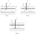
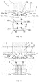
- FIG 1 shows a donor substrate 1, for example a glass wafer, with a blister forming layer 2 on a surface of the donor substrate and an adhesive layer 3 on blister forming layer.
- a donor substrate for example a glass wafer
- an adhesive layer 3 on blister forming layer.
- the adhesive layer 3 may be omitted if the blister forming layer 2 itself has the required adhesive properties for attaching components.
- Attached to the adhesive layer 3 is an array of components 4, which may for example be micro-sized chips 4 having a square shaped cross-section with a lateral dimension of about 100 ⁇ m.
- the components 4 may have various shapes and dimensions. For example, square or rectangular chips may be used with lateral dimensions ranging between a few tens of micrometres to hundreds of micrometres or more. The thickness may be up to 50 ⁇ m or even 100 ⁇ m or more.
- the aim of the method is to transfer the components (e.g. chips) to a receiver substrate 5 provided, e.g. mounted, such that it faces the donor substrate.
- the receiver substrate 5 comprises an adhesive layer 6 to which the chips 4 will adhere when they are transferred. Any adhesive layer 6 that is applicable in existing LIFT techniques can be used here.
- the adhesive layer 6 may be a patterned layer, for example comprising adhesive material only at the locations where the chips 4 are to be received.
- the receiver substrate 5 may be a substrate to which the chips 4 are to be permanently attached, or a carrier substrate to which the chips are to be temporarily attached.
- the donor substrate 1 and the receiver substrate 5 are preferably aligned with respect to each other and possibly maintained at a given distance by one or more spacers (not shown) or by using motorized stages to which the donor substrate and the receiver substrate are respectively attached, so as to create an air gap between the two substrates, as generally known from existing LIFT-based techniques.
- a laser beam 7 is directed at one of the chips 4 from the back side of the donor substrate 1, i.e. from the side of the donor substrate opposite to the side where the chips 4 are located, i.e. from the side of the donor substrate 1 opposite to the side facing the receiver substrate 5.
- the laser beam 7 is directed such that it has a footprint on the donor substrate at the location of the chip, i.e. at a location within the contact area between the component and the blister forming layer.
- the footprint of the laser beam is defined as the projection of the laser beam on the donor substrate.
- the laser beam is preferably a pulsed laser beam.
- a single laser pulse is applied for releasing the chip.
- the laser beam is directed at a spot 8 at the centre of the initial contact area between the chip 4 that is to be irradiated and the blister forming layer 2 (hereafter 'the contact area').
- the spot thus corresponds to the footprint of the laser beam.
- Geometrical centrality is however not required and the position of the spot 8 may vary according to different embodiments, as will be further described.
- the contact area corresponds to the full area of the chip 4.
- the location of the spot 8, as well as the size and shape of the laser beam 7 may vary according to different embodiments, as will be explained further.
- the blister forming layer 2 is vaporized by the interaction with the laser beam, and the vapour causes the formation of a blister 10 that is inflated by the pressure of the vapour.
- the sides of the chip 4 are released from the adhesive layer 3 / blister forming layer 2, due to the curvature of the blister 10, so that the contact area between the chip 4 and the adhesive layer 3 / blister forming layer 2 becomes smaller compared to the initial contact area at the initial moment of impact of the laser beam (illustrated in FIG 1 ).
- the blister 10 continues to inflate until a small opening, i.e.
- a nozzle 11 is created, resulting in the release of a small, narrow jet 12 of vaporized material.
- the jet 12 releases the chip 4 from the blister forming layer in the remaining contact area and propels the chip 4 towards the receiver substrate 5, where it is attached to the adhesive receiving layer 6 present on the receiver substrate 5 ( Fig 2c ).
- the jet 12 is narrow as compared to the contact area, which enhances the thrust force in the direction of the receiver substrate 5 relative to drag forces working in the transverse direction.
- the narrow jet 12 is thus advantageous when it comes to optimizing the directionality of the chip 4 during its transfer to the receiver substrate 5, and hence obtaining a minimum deviation from the desired location at which the chip 4 is to land on the receiver substrate 5, i.e. hence obtaining accurate positioning of the chip 4 on the receiver substrate 5.
- the nozzle 11 is formed at a predefined location within the contact area.
- Different ways are possible for defining the location of the nozzle, in accordance with different respective embodiments of the invention, described hereafter.
- the chips 4 are attached to the blister forming layer 2 by an adhesive layer 3.
- the descriptions of these embodiments are valid also when the blister forming layer is itself adhesive, wherein the adhesive layer 3 may be omitted.
- the blister-forming layer 2 is a so-called dynamic release layer or DRL 15, i.e. a single layer of dynamic release material, possibly extending across the full area of the donor substrate 1, in any case across an area that is large compared to the contact area.
- a dynamic release material is defined as a material that can be vaporized through the interaction between the material and a laser beam impinging on the material.
- dynamic release materials are non-transparent or not fully transparent to the laser light of the impinging laser beam 7, but these materials have the property of absorbing the laser light to the point where the material is vaporized, thereby forming a gas of vaporized material, at the location of impact of the laser beam.
- Materials of this type are known from the above-described LIFT techniques.
- a suitable material is for example polyimide 2610 produced by HD MicroSystems TM . Materials which are transparent to the laser light may nevertheless be vaporized by a laser when the laser has specific properties.
- a material that is vaporized in this way is therefore also defined as a dynamic release material, and a layer of this material is a dynamic release layer.
- the chips 4 are attached to the DRL 15 through the adhesive layer 3 which may for example be a BCB (benzocyclobutene) layer.
- the diameter of the laser beam 7 is small relative to the initial contact area between the chip 4 and the dynamic release layer 2 and adhesive layer 3.
- the spot 8 irradiated by the laser beam (the footprint of the laser beam) is located near the centre of said initial contact area (as shown in FIG 1 ).
- the spot 8 is preferably located in line with the centre of gravity of the component that is to be transferred. In many cases, this corresponds to the centre of the contact area, as schematically illustrated in the drawings.
- the beam 7 may be deliberately directed at an out-of-centre spot within the contact area.
- the laser beam 7 causes the vaporization of the DRL 15 to occur locally at a central vaporized area 16 within the contact area, created upon impact of the laser beam.
- a nozzle 11 is formed at the location of this central area 16, as illustrated in FIG 3c , such that the a jet 12 of vaporized material is produced by vaporized material exiting the blister 10 via the nozzle 11, causing release of the chip 4, such that the chip is propelled towards the receiver substrate 5 by the jet 12.
- the laser beam 7 may be a Gaussian beam, i.e. a monochromatic beam whose amplitude envelope in the transverse plane is determined by a Gaussian function.
- the diameter of a Gaussian beam is defined within the present context as the width corresponding to the full width at half maximum of the amplitude (FWHM).
- the laser beam may also be a windowed 'flat-top' beam, whose amplitude profile is flat. The diameter of the beam is then defined essentially equal to the width of the amplitude profile.
- a Gaussian beam having a diameter of about 30 ⁇ m, wavelength 355nm, and a pulse energy of about 9 ⁇ J is appropriate in accordance with this embodiment of the invention, in combination with a DRL 15 in the form of a polyimide film having a thickness between 1 and 3 ⁇ m, for example 1.4 ⁇ m, and a very thin adhesive layer 3.
- a BCB adhesive 3 with a thickness of less than 500 nm is suitable for placing chips 4 of the size indicated above, for example applying an air gap between the donor substrate and the receiver substrate of about 200 ⁇ m (i.e. about 120 ⁇ m between the chip 4 and the receiver substrate).
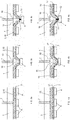
- FIG 4a to FIG 4c illustrate an exemplary embodiment wherein the diameter of the laser beam 7 defines the location of the nozzle 11, as in the example shown in FIG 3a to FIG 3c , but wherein the blister forming layer 2 is a stack of a DRL 15 and a non-vaporizing layer 17 that has suitable properties for forming a blister in terms of its elasticity and thickness, but that itself does not react with the laser beam 7, i.e. the material of this non-vaporizing layer 17 is not vaporized by the laser light.
- the vaporized area 16 is formed by the local vaporization of the DRL 15, and as shown in FIG 4c , the nozzle 11 is formed by an opening created through the non-vaporizing layer 17 at the location of the vaporized area 16.
- the nozzle 11 is formed at this location, because the local vaporization of the DRL 15 in vaporized area 16 creates a weak spot of the complete blister forming layer 2 at this location.
- the non-vaporizing layer 17 may for example be a layer of PDMS (polydimethylsiloxane), which is transparent to laser light of wavelength 355 nm and may thus be combined with a polyimide DRL layer 15 when laser light at this wavelength is used.
- the non-vaporizing layer 17 may itself be a polyimide layer that is transparent to a laser light at another wavelength, for example 1063 nm, when laser light at this different wavelength is used, in combination with a DRL 15 that is vaporized at this wavelength.
- the location of the nozzle 11 is defined by a structural feature of the blister forming layer 2, integrated in this layer prior to the application of the laser beam 7.
- FIG 5a to FIG 5c A first example of such an embodiment is illustrated in FIG 5a to FIG 5c .
- the blister forming layer 2 is a DRL 15, with a local indentation 20 formed in the DRL 15, near the centre of the contact area between the blister forming layer 2 and the the chips 4, in the surface of the DRL 15 opposite the side attached to the donor substrate 1, i.e. opposite the surface facing the donor substrate 1.
- the local indentation 20 thus forms an area wherein the DRL 15 is locally thinner.
- This locally thinner area may have a circular cross section as seen in the plane section view included in FIG 5a , but other cross sections or shapes of the indentation 20 are possible.
- the adhesive layer 3 is interrupted in this area, but it may also fill the volume of the indentation 20, as further illustrated.
- the indentation 20 is small relative to the lateral dimensions of the chip 4.
- the indentation 20 may have a diameter in this plane of about 30-40 ⁇ m if the chip's lateral dimensions are 90 ⁇ m x 130 ⁇ m.
- the indentation 20 may be located out-of-centre of the contact area, for example when the centre of gravity of the chip 4 is not in line with the centre of the contact area.
- the laser beam 7 may be a beam having a small diameter relative to the contact area.
- the laser beam may be directed at the location of the indentation 20, as is the case in FIG 5a .
- local vaporization of the DRL 15 occurs, as described above, and a nozzle 11 is formed at the location of the indentation 20, which coincides with local vaporization area 16.
- the local indentation 20 creates a more pronounced weak spot at the desired nozzle location, decreasing the risk that the nozzle would form at another spot, due to irregular blister growth or other factors.
- the laser beam 7 may also have a larger diameter, for example a diameter in the order of the chip's size, as illustrated in FIG 5d .
- the nozzle 11 is formed at the location of the indentation 20, because this local indentation creates a weak spot in the blister forming layer 2 at the desired nozzle location. Therefore, according to this embodiment, the indentation 20 determines the location where the nozzle 11 is formed, regardless of whether the laser beam is narrow or wide.
- the indentation 20 shown in FIG 5a to FIG 5d is referred to in the present context as a 'point-type' indentation, defined as a small, narrowly localized indentation that gives rise to a point-type nozzle 11 and a line-type jet 12, i.e. a narrow stream of gas issuing from a small point-type location of the blister 10.
- the nozzle may however also be a line-shaped nozzle, which can be achieved by creating a line-shaped indentation in the DRL 15.
- FIG 5e illustrates an embodiment wherein the indentation 20 is shaped as a circular line (a ring).
- the nozzle 11 is a line-type nozzle formed along the circumference of the ring
- the jet 12 is a sheet-type jet issued from the circular nozzle 11.
- a line-type nozzle may be created that replicates, fully or partially and on a smaller scale, the irregular shape of the contact area, for example in a central portion of said contact area.
- a line-type indentation 20 having said irregular shape is produced in the blister-forming layer prior to attaching the component to the donor substrate.
- the sheet-type jet may be adapted to the shape of the contact area.
- FIG 6a to FIG 6c illustrate another example of an embodiment wherein the location where the nozzle 11 is formed is defined by the presence of a local indentation in the blister forming layer.
- the blister forming layer 2 is a stack of a DRL 15 and a non-vaporizing layer 17, and the indentations 20 are formed in said non-vaporizing layer 17.
- the indentations 20 may also reach down to the DRL 15, passing through the complete thickness of the non-vaporizing layer 17.
- the indentations 20 are produced in the DRL 15 before the chips 4 are placed thereon.
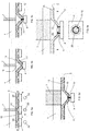
- FIG 7a to FIG 7d show an exemplary method for producing a substrate for use in such embodiment.
- a donor substrate 1 is provided (and preferably cleaned), followed by the deposition of a DRL 15.
- a polyimide DRL 15 may be applied by spin coating.
- the DRL 15 is locally thinned ( FIG 7c ), which may be done by a laser treatment or by a lithography and etch step, thus forming the local indentations 20.
- the adhesive layer 3 is then applied on the DRL15.
- FIG 7e illustrates attaching components (chips) 4 to the substrate of FIG 7d by adhesion to the blister forming layer 2, with the contact area between the components and the blister forming layer overlaying a local indentation 20.
- each of the chips 4 is to be aligned to the location of an indentation 20, preferably such that the indentation corresponds to the centre of the contact area between the chip 4 and the adhesive layer 3.
- the location of the indentation 20 relative to the chip 4 may be deliberately chosen in an out-of-centre spot of the contact area.
- the adhesive layer 3 is applied first on the DRL 15 ( FIG 8c ) and the local indentations 20 are formed thereafter ( FIG 8d ), such that the adhesive layer 3 is automatically removed from the DRL 15 in the area where the local indentations 20 are formed.
- Possible methods for preparing the donor substrate 1 to thereby produce a substrate for use in a method as illustrated in FIG 6a to FIG 6c are similar to the methods illustrated in FIG 7a to FIG 7d and in FIG 8a to FIG 8d , but with the non-vaporizing layer 17 being patterned to form the indentations 20 therein, while the DRL 15 itself remains intact.
- the location of the nozzle is defined by the presence of (the location of) a local reinforcing element on the blister forming layer 2.
- FIG 9a to FIG 9d An example of such an embodiment is illustrated in FIG 9a to FIG 9d , wherein the blister forming layer 2 is a dynamic release layer 15.
- a ring-shaped reinforcing element 25 is present on the DRL 15, on the surface of the DRL opposite to the surface facing the donor substrate 1.
- the ring-shaped reinforcing element 25 is a patterned layer of reinforcing material comprising an open area its centre (central opening) and a layer of reinforcing material around said open area.
- the laser beam 7 is directed to the central opening of the ring-shaped reinforcing element.
- the nozzle is then created at a spot 8 that is coaxial with the centre of this ring-shaped reinforcing element 25.
- the reinforcing element 25 may be formed of metal or of a polymer with a higher elasticity modulus than the DRL 15. It may be formed by depositing a layer of said metal or polymer (a layer of reinforcing material) on the DRL and patterning the layer by lithography and etching, prior to the formation of the adhesive layer 3. As an alternative to lithography and etching, additive techniques may be used for forming the reinforcing element 25, such as for example printing.
- FIG 9a to FIG 9c a laser beam 7 having a small diameter relative to the contact area may be used.
- FIG 9b and FIG 9c show the local vaporization of the DRL 15 and the formation of a nozzle 11 at the central open area of the local reinforcing element 25.
- the reinforcing element 25 ensures that the nozzle 11 is formed at a location corresponding to the open area (in the example shown the centre) of the reinforcing element 25.
- the laser beam 7 may also have a larger diameter, for example a diameter in the order of the size of the components 4.
- the reinforcing element 25 is somewhat larger than the footprint of the laser, ensuring that the nozzle 11 is formed in the open area at its centre rather than at any other location of the expanding blister 10.
- the nozzle is formed at the location of the open area of the reinforcing element 25.
- the location of the nozzle is defined by the location of the open area, regardless of whether the laser beam is narrow or wide.
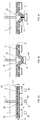
- FIG 10a to FIG 10c illustrate an embodiment wherein the location of the nozzle is defined by the location of an open area of a reinforcing element 25 formed on a blister forming layer 2, wherein the blister forming layer 2 is a stack of a DRL 15 and a non-vaporizing layer 17 on the DRL 15.
- the shape and dimensions of the reinforcing element 25 are not limited to the ring-shape shown in the drawings.
- the reinforcing element 25 at least has an open area that determines the location of the nozzle, but the surrounding material (patterned layer of reinforcing material) of the reinforcing element may have any suitable shape and/or any suitable dimensions.
- the patterned layer of reinforcing material preferably has a closed circular or polygonal shape, but a non-closed shape such as a non-closed ring formed of separate strips may also have the desired effect. Preferred characteristics in terms of the shape or size of the reinforcing element may depend on the thickness and composition of the blister forming layer, the laser wavelength and/or laser power, or other parameters of the method.
- the reinforcing element 25 may be have an open area located in the centre of the contact area, or it may have an open area located out-of-centre relative to the contact area, for example as a function of the location of the centre of gravity of the component to be transferred.
- the reinforcing element 25 may also be combined with a local indentation 20 in the DRL 15 or in the non-vaporizing layer 17.
- the local indentation 20 and the reinforcing element 25 are provided coaxially with respect to each other.
- the reinforcing element 25 may comprise two strips of reinforcing material, placed on either side of the indentation 20.
- the DRL itself is patterned such that a local patch 26 of dynamic release material is present in at least part of the contact area with each chip 4.
- This may be achieved by providing a DRL 15 on the entire surface of the donor substrate 1 (as in FIG 7b and FIG 8b ), followed by patterning this layer by lithography and etching.
- the patches 26 may have a round shape as illustrated in the plane section view included in FIG 11a , but other shapes are possible as well.
- the blister-forming layer 2 comprises the patches 26 of dynamic release material and the non-vaporizing layer 17.
- the laser beam 7 then causes vaporization of substantially the complete patch 26 of DRL material, and the local indentation 20 defines the location of the nozzle 11, as illustrated in FIG 11b and FIG 11c .
- the laser diameter may be larger, as the indentation 20 defines the location of the nozzle 11, irrespective of the size of the footprint of the laser.
- patches 26 of dynamic release material may also be applied in combination with reinforcing elements 25 as described above, and with the combined application of local indentations 20 and reinforcing elements 25 (i.e. patches 26, local indentations 20 and reinforcing elements 25 combined in one embodiment).
- more than one nozzle is formed in the contact area between the blister forming layer and a component to be placed and the donor substrate.
- FIG 12 Such an embodiment is illustrated in FIG 12 , showing an example wherein two nozzles are created within the contact area of a chip 4 with a rectangular cross-section.
- the nozzles are created by directing two laser beams 7a and 7b simultaneously to spots 8a and 8b respectively, located within the contact area between the chip 4 and the adhesive layer 3 present on the blister-forming layer 2.
- the laser beams may be obtained by splitting a single laser beam.
- the nozzles are distributed evenly across the initial contact area, so that multiple blisters 10a and 10b are formed, resulting in multiple nozzles 11a and 11b and multiple jets 12a and 12b which propel the chip 4 towards the receiver substrate 5.
- This embodiment can be applied for any component shape, using as many lasers as required as a function of the dimensions of the contact area between the component and the donor substrate.
- the nozzle locations may be defined according to any one of the embodiments described with respect to FIGs 3 to 11 .
- This embodiment is not only useful for transferring larger components, but also for transferring components with irregular, e.g. asymmetrical shapes of the contact area, or components which have a fragile structure at their centre (for example a microlens), so that the nozzles may be placed at regular distances around said fragile structure.
- a single laser 7 is applied to a relatively large chip 4, and multiple nozzles are created for propelling the chip towards the receiver substrate.
- This embodiment preferably uses a broad laser beam 7, for example a laser beam having a footprint in the order of the initial contact area between the component 4 and the dynamic release layer, combined with multiple local indentations and/or multiple reinforcing elements, which define the location of the nozzles.
- a broad laser beam 7 for example a laser beam having a footprint in the order of the initial contact area between the component 4 and the dynamic release layer, combined with multiple local indentations and/or multiple reinforcing elements, which define the location of the nozzles.
- four local indentations 20a to 20d are arranged in a square pattern.
- the laser beam creates a blister 10 which gives rise to the more or less simultaneous formation of four nozzles 11a to 11d, after which four jets 12a to 12d propel the chip 4 towards the receiver substrate 5.
- This embodiment is not only useful for transferring relatively large components, but also for transferring components with irregular shapes of the contact area, or components which have a fragile structure at their centre, so that the nozzles may be placed at a distance from said fragile structure, e.g. at equal distances around said fragile structure.
- FIG 14 illustrates an example wherein two indentations 20a and 20b are used, both having the shape of a straight line, from one end of the chip 4 to the other and placed symmetrically with respect to the centre of the chip 4. This results in the formation of two line-type nozzles 11a and 11b, and two straight sheet-type jets 12a and 12b which propel the chip towards the receiver substrate 5.
- a number of parameters may need to be optimized, such as the dimensions of the indentations 20 and/or the reinforcing elements 25, the thickness of the DRL 15 and (if present) the non-vaporizing layer 17, the material of these layers, the type and thickness of the adhesive layer 3 (if present).
- These parameters may differ as a function of the size and shape of the components 4 that are to be transferred, the applied laser power, the laser diameter etc.
- the optimization of these parameters is therefore dependent on the specific case in terms especially of the component type and dimensions. This optimization is a process that can be performed by the skilled person on the basis of a reasonable number of trials.
- suitable parameters in the context of the embodiment of FIG 5 has been given above.
- the spot 8 to which the laser beam 7 is directed has a circular shape in embodiments of the present invention described above and illustrated in the drawings (for example FIG 5a , FIG 6a ), due to the circular shape (as seen in cross-section) of the laser beam 7 and the circular shape of its footprint on the donor substrate.
- Other shapes of the footprint of the laser beam 7 and hence other shapes of the spot 8 are possible, however.
- the shape of the laser beam may be adapted to the shape of the component and/or of the contact area, or to the number and position of the indentations and/or the reinforcing elements.
- a circular laser spot can be shaped into an elliptical laser spot, resulting in an elliptical footprint on the donor substrate, thereby providing a better overlap with a rectangular chip to be transferred (for example for an embodiment according to FIG 3 of FIG 4 ), by orienting the elliptical spot with its largest dimension in the length direction of the chip.
- the laser beam 7 may be shaped so as to overlap more closely the locations of the indentations and/or reinforcing elements, which can be advantageous compared to a circular spot.
- a circular spot overlapping a row of two or more indentations 20 provided in the length direction of a rectangular chip 4 needs to have a large diameter, resulting in a blister that is oversized in the transverse direction (perpendicular to the length direction), which threatens to impact adjacent chips unless the chips are placed at a sufficiently large distance from each other in said transverse direction.
- the footprint of the laser is shaped to have an elliptical shape extending in the length direction of the chip, the blister is shaped according to the elliptical shape, and chips can be placed closer to each other on the donor substrate.
- the method of the invention allows to achieve placement of a large number of components at high throughput rates, as the laser can be displaced quickly from one component to a next one when a plurality of small components attached to the donor substrate is to be transferred to a receiver substrate. Throughput rates of several hundred to tens of thousands of components per second are achievable.
- the method is applicable for example for:
Landscapes
- Physics & Mathematics (AREA)
- Optics & Photonics (AREA)
- Engineering & Computer Science (AREA)
- Plasma & Fusion (AREA)
- Mechanical Engineering (AREA)
- Chemical & Material Sciences (AREA)
- Chemical Kinetics & Catalysis (AREA)
- General Chemical & Material Sciences (AREA)
- Oil, Petroleum & Natural Gas (AREA)
- Physical Vapour Deposition (AREA)
- Laser Beam Processing (AREA)
Priority Applications (3)
| Application Number | Priority Date | Filing Date | Title |
|---|---|---|---|
| EP20182867.0A EP3933902B1 (fr) | 2020-06-29 | 2020-06-29 | Procédé de positionnement de composants sur un substrat |
| US18/000,551 US12456641B2 (en) | 2020-06-29 | 2021-06-23 | Method for positioning components on a substrate and substrates suitable for the method |
| PCT/EP2021/067266 WO2022002733A1 (fr) | 2020-06-29 | 2021-06-23 | Procédé de positionnement de composants sur un substrat et substrats appropriés pour le procédé |
Applications Claiming Priority (1)
| Application Number | Priority Date | Filing Date | Title |
|---|---|---|---|
| EP20182867.0A EP3933902B1 (fr) | 2020-06-29 | 2020-06-29 | Procédé de positionnement de composants sur un substrat |
Publications (2)
| Publication Number | Publication Date |
|---|---|
| EP3933902A1 true EP3933902A1 (fr) | 2022-01-05 |
| EP3933902B1 EP3933902B1 (fr) | 2023-05-03 |
Family
ID=71409108
Family Applications (1)
| Application Number | Title | Priority Date | Filing Date |
|---|---|---|---|
| EP20182867.0A Active EP3933902B1 (fr) | 2020-06-29 | 2020-06-29 | Procédé de positionnement de composants sur un substrat |
Country Status (3)
| Country | Link |
|---|---|
| US (1) | US12456641B2 (fr) |
| EP (1) | EP3933902B1 (fr) |
| WO (1) | WO2022002733A1 (fr) |
Families Citing this family (4)
| Publication number | Priority date | Publication date | Assignee | Title |
|---|---|---|---|---|
| US11973054B2 (en) * | 2021-05-06 | 2024-04-30 | Stroke Precision Advanced Engineering Co., Ltd. | Method for transferring electronic device |
| JP7733602B2 (ja) * | 2022-03-28 | 2025-09-03 | 東レエンジニアリング株式会社 | 転写装置および転写方法 |
| US20230317687A1 (en) * | 2022-03-31 | 2023-10-05 | Intel Corporation | Micro-led display architecture for high volume manufacturing |
| KR20250164199A (ko) * | 2023-03-29 | 2025-11-24 | 토레 엔지니어링 가부시키가이샤 | 소자 전사 장치 및 소자 전사 방법 |
Citations (2)
| Publication number | Priority date | Publication date | Assignee | Title |
|---|---|---|---|---|
| US20060081572A1 (en) | 2002-05-24 | 2006-04-20 | Weekamp Johannus W | Method suitable for transferring a component supported by a carrier to a desired position on a substrate, and a device designed for this |
| WO2012142177A2 (fr) | 2011-04-11 | 2012-10-18 | Ndsu Research Foundation | Transfert assisté par laser sélectif de composants discrets |
Family Cites Families (4)
| Publication number | Priority date | Publication date | Assignee | Title |
|---|---|---|---|---|
| WO2012033147A1 (fr) | 2010-09-09 | 2012-03-15 | 学校法人 東北学院 | Capteur de concentration de gaz spécifié |
| CN107107600B (zh) | 2014-08-05 | 2021-07-27 | 尤尼卡尔塔股份有限公司 | 设置便于组装的超小或超薄分立元件 |
| TWI889995B (zh) * | 2016-01-15 | 2025-07-11 | 荷蘭商庫力克及索發荷蘭公司 | 放置超小或超薄之離散組件 |
| CN121335436A (zh) * | 2019-02-15 | 2026-01-13 | 库力索法荷兰有限公司 | 用于组装离散组件的动态释放带 |
-
2020
- 2020-06-29 EP EP20182867.0A patent/EP3933902B1/fr active Active
-
2021
- 2021-06-23 US US18/000,551 patent/US12456641B2/en active Active
- 2021-06-23 WO PCT/EP2021/067266 patent/WO2022002733A1/fr not_active Ceased
Patent Citations (2)
| Publication number | Priority date | Publication date | Assignee | Title |
|---|---|---|---|---|
| US20060081572A1 (en) | 2002-05-24 | 2006-04-20 | Weekamp Johannus W | Method suitable for transferring a component supported by a carrier to a desired position on a substrate, and a device designed for this |
| WO2012142177A2 (fr) | 2011-04-11 | 2012-10-18 | Ndsu Research Foundation | Transfert assisté par laser sélectif de composants discrets |
Non-Patent Citations (1)
| Title |
|---|
| "Proceedings of SPIE", vol. 6261, 7 June 2006, SPIE, 1000 20th St. Bellingham WA 98225-6705 USA, ISBN: 978-1-5106-3927-0, ISSN: 0277-786X, article NATALLIA S. KARLITSKAYA ET AL: "Laser propulsion of microelectronic components: releasing mechanism investigation", pages: 62612P - 1, XP055649690, DOI: 10.1117/12.673815 * |
Also Published As
| Publication number | Publication date |
|---|---|
| US12456641B2 (en) | 2025-10-28 |
| EP3933902B1 (fr) | 2023-05-03 |
| WO2022002733A1 (fr) | 2022-01-06 |
| US20230290664A1 (en) | 2023-09-14 |
Similar Documents
| Publication | Publication Date | Title |
|---|---|---|
| US12456641B2 (en) | Method for positioning components on a substrate and substrates suitable for the method | |
| US12431381B2 (en) | Light induced selective transfer of components between substrates | |
| US9862141B2 (en) | Selective laser-assisted transfer of discrete components | |
| CN102730627B (zh) | 在基板中形成凹部的方法 | |
| US9111983B1 (en) | Methods for removing adhesive layers from semiconductor wafers | |
| US20090225131A1 (en) | Fluid Ejector Structure and Fabrication Method | |
| US7767574B2 (en) | Method of forming micro metal bump | |
| JP2018537699A5 (fr) | ||
| EP3890979B1 (fr) | Transfert avant induit par laser haute résolution | |
| JP2002182580A (ja) | 素子の選択転写方法、画像表示装置の製造方法及び液晶表示装置の製造方法 | |
| EP4053888A1 (fr) | Pile de libération multicouche pour le transfert de composants induit par la lumière | |
| US20250204119A1 (en) | Multi-layer release stack for light induced transfer of components | |
| JP2004520981A (ja) | 液滴付着装置用ノズル板 | |
| JP7819950B2 (ja) | 硬質基材から可撓性マイクロ電子デバイスを製作し分離するための技術 | |
| WO2023190395A1 (fr) | Dispositif de transfert et procédé de transfert | |
| CN102388440A (zh) | 用于处理基板的方法、用于生产半导体芯片的方法和用于生产具有树脂粘结剂层的半导体芯片的方法 | |
| CN100389958C (zh) | 制造喷嘴板的方法 | |
| JPH07314692A (ja) | インクジェットノズルの製造方法 | |
| CN117136429A (zh) | 用于组件的光诱导转移的多层释放叠层 | |
| JP2021068849A (ja) | モールド、成形装置、および物品の製造方法 | |
| WO2024122552A1 (fr) | Procédé de transfert |
Legal Events
| Date | Code | Title | Description |
|---|---|---|---|
| PUAI | Public reference made under article 153(3) epc to a published international application that has entered the european phase |
Free format text: ORIGINAL CODE: 0009012 |
|
| STAA | Information on the status of an ep patent application or granted ep patent |
Free format text: STATUS: THE APPLICATION HAS BEEN PUBLISHED |
|
| AK | Designated contracting states |
Kind code of ref document: A1 Designated state(s): AL AT BE BG CH CY CZ DE DK EE ES FI FR GB GR HR HU IE IS IT LI LT LU LV MC MK MT NL NO PL PT RO RS SE SI SK SM TR |
|
| B565 | Issuance of search results under rule 164(2) epc |
Effective date: 20210114 |
|
| STAA | Information on the status of an ep patent application or granted ep patent |
Free format text: STATUS: REQUEST FOR EXAMINATION WAS MADE |
|
| 17P | Request for examination filed |
Effective date: 20220524 |
|
| RBV | Designated contracting states (corrected) |
Designated state(s): AL AT BE BG CH CY CZ DE DK EE ES FI FR GB GR HR HU IE IS IT LI LT LU LV MC MK MT NL NO PL PT RO RS SE SI SK SM TR |
|
| RIC1 | Information provided on ipc code assigned before grant |
Ipc: H01L 33/00 20100101ALN20220920BHEP Ipc: H01L 21/683 20060101AFI20220920BHEP |
|
| RIC1 | Information provided on ipc code assigned before grant |
Ipc: H01L 33/00 20100101ALN20221114BHEP Ipc: H01L 21/683 20060101AFI20221114BHEP |
|
| RIC1 | Information provided on ipc code assigned before grant |
Ipc: H01L 33/00 20100101ALN20221118BHEP Ipc: H01L 21/683 20060101AFI20221118BHEP |
|
| GRAP | Despatch of communication of intention to grant a patent |
Free format text: ORIGINAL CODE: EPIDOSNIGR1 |
|
| STAA | Information on the status of an ep patent application or granted ep patent |
Free format text: STATUS: GRANT OF PATENT IS INTENDED |
|
| RIN1 | Information on inventor provided before grant (corrected) |
Inventor name: VAN STEENBERGE, GEERT Inventor name: STERKEN, TOM |
|
| INTG | Intention to grant announced |
Effective date: 20230102 |
|
| RAP3 | Party data changed (applicant data changed or rights of an application transferred) |
Owner name: UNIVERSITEIT GENT Owner name: IMEC VZW |
|
| GRAS | Grant fee paid |
Free format text: ORIGINAL CODE: EPIDOSNIGR3 |
|
| GRAA | (expected) grant |
Free format text: ORIGINAL CODE: 0009210 |
|
| STAA | Information on the status of an ep patent application or granted ep patent |
Free format text: STATUS: THE PATENT HAS BEEN GRANTED |
|
| AK | Designated contracting states |
Kind code of ref document: B1 Designated state(s): AL AT BE BG CH CY CZ DE DK EE ES FI FR GB GR HR HU IE IS IT LI LT LU LV MC MK MT NL NO PL PT RO RS SE SI SK SM TR |
|
| REG | Reference to a national code |
Ref country code: GB Ref legal event code: FG4D |
|
| REG | Reference to a national code |
Ref country code: AT Ref legal event code: REF Ref document number: 1565393 Country of ref document: AT Kind code of ref document: T Effective date: 20230515 Ref country code: CH Ref legal event code: EP |
|
| REG | Reference to a national code |
Ref country code: DE Ref legal event code: R096 Ref document number: 602020010292 Country of ref document: DE |
|
| REG | Reference to a national code |
Ref country code: IE Ref legal event code: FG4D |
|
| REG | Reference to a national code |
Ref country code: NL Ref legal event code: FP |
|
| REG | Reference to a national code |
Ref country code: LT Ref legal event code: MG9D |
|
| REG | Reference to a national code |
Ref country code: AT Ref legal event code: MK05 Ref document number: 1565393 Country of ref document: AT Kind code of ref document: T Effective date: 20230503 |
|
| P01 | Opt-out of the competence of the unified patent court (upc) registered |
Effective date: 20230914 |
|
| PG25 | Lapsed in a contracting state [announced via postgrant information from national office to epo] |
Ref country code: SE Free format text: LAPSE BECAUSE OF FAILURE TO SUBMIT A TRANSLATION OF THE DESCRIPTION OR TO PAY THE FEE WITHIN THE PRESCRIBED TIME-LIMIT Effective date: 20230503 Ref country code: PT Free format text: LAPSE BECAUSE OF FAILURE TO SUBMIT A TRANSLATION OF THE DESCRIPTION OR TO PAY THE FEE WITHIN THE PRESCRIBED TIME-LIMIT Effective date: 20230904 Ref country code: NO Free format text: LAPSE BECAUSE OF FAILURE TO SUBMIT A TRANSLATION OF THE DESCRIPTION OR TO PAY THE FEE WITHIN THE PRESCRIBED TIME-LIMIT Effective date: 20230803 Ref country code: ES Free format text: LAPSE BECAUSE OF FAILURE TO SUBMIT A TRANSLATION OF THE DESCRIPTION OR TO PAY THE FEE WITHIN THE PRESCRIBED TIME-LIMIT Effective date: 20230503 Ref country code: AT Free format text: LAPSE BECAUSE OF FAILURE TO SUBMIT A TRANSLATION OF THE DESCRIPTION OR TO PAY THE FEE WITHIN THE PRESCRIBED TIME-LIMIT Effective date: 20230503 |
|
| PG25 | Lapsed in a contracting state [announced via postgrant information from national office to epo] |
Ref country code: RS Free format text: LAPSE BECAUSE OF FAILURE TO SUBMIT A TRANSLATION OF THE DESCRIPTION OR TO PAY THE FEE WITHIN THE PRESCRIBED TIME-LIMIT Effective date: 20230503 Ref country code: PL Free format text: LAPSE BECAUSE OF FAILURE TO SUBMIT A TRANSLATION OF THE DESCRIPTION OR TO PAY THE FEE WITHIN THE PRESCRIBED TIME-LIMIT Effective date: 20230503 Ref country code: LV Free format text: LAPSE BECAUSE OF FAILURE TO SUBMIT A TRANSLATION OF THE DESCRIPTION OR TO PAY THE FEE WITHIN THE PRESCRIBED TIME-LIMIT Effective date: 20230503 Ref country code: LT Free format text: LAPSE BECAUSE OF FAILURE TO SUBMIT A TRANSLATION OF THE DESCRIPTION OR TO PAY THE FEE WITHIN THE PRESCRIBED TIME-LIMIT Effective date: 20230503 Ref country code: IS Free format text: LAPSE BECAUSE OF FAILURE TO SUBMIT A TRANSLATION OF THE DESCRIPTION OR TO PAY THE FEE WITHIN THE PRESCRIBED TIME-LIMIT Effective date: 20230903 Ref country code: HR Free format text: LAPSE BECAUSE OF FAILURE TO SUBMIT A TRANSLATION OF THE DESCRIPTION OR TO PAY THE FEE WITHIN THE PRESCRIBED TIME-LIMIT Effective date: 20230503 Ref country code: GR Free format text: LAPSE BECAUSE OF FAILURE TO SUBMIT A TRANSLATION OF THE DESCRIPTION OR TO PAY THE FEE WITHIN THE PRESCRIBED TIME-LIMIT Effective date: 20230804 |
|
| PG25 | Lapsed in a contracting state [announced via postgrant information from national office to epo] |
Ref country code: FI Free format text: LAPSE BECAUSE OF FAILURE TO SUBMIT A TRANSLATION OF THE DESCRIPTION OR TO PAY THE FEE WITHIN THE PRESCRIBED TIME-LIMIT Effective date: 20230503 |
|
| PG25 | Lapsed in a contracting state [announced via postgrant information from national office to epo] |
Ref country code: SK Free format text: LAPSE BECAUSE OF FAILURE TO SUBMIT A TRANSLATION OF THE DESCRIPTION OR TO PAY THE FEE WITHIN THE PRESCRIBED TIME-LIMIT Effective date: 20230503 |
|
| PG25 | Lapsed in a contracting state [announced via postgrant information from national office to epo] |
Ref country code: SM Free format text: LAPSE BECAUSE OF FAILURE TO SUBMIT A TRANSLATION OF THE DESCRIPTION OR TO PAY THE FEE WITHIN THE PRESCRIBED TIME-LIMIT Effective date: 20230503 Ref country code: SK Free format text: LAPSE BECAUSE OF FAILURE TO SUBMIT A TRANSLATION OF THE DESCRIPTION OR TO PAY THE FEE WITHIN THE PRESCRIBED TIME-LIMIT Effective date: 20230503 Ref country code: RO Free format text: LAPSE BECAUSE OF FAILURE TO SUBMIT A TRANSLATION OF THE DESCRIPTION OR TO PAY THE FEE WITHIN THE PRESCRIBED TIME-LIMIT Effective date: 20230503 Ref country code: EE Free format text: LAPSE BECAUSE OF FAILURE TO SUBMIT A TRANSLATION OF THE DESCRIPTION OR TO PAY THE FEE WITHIN THE PRESCRIBED TIME-LIMIT Effective date: 20230503 Ref country code: DK Free format text: LAPSE BECAUSE OF FAILURE TO SUBMIT A TRANSLATION OF THE DESCRIPTION OR TO PAY THE FEE WITHIN THE PRESCRIBED TIME-LIMIT Effective date: 20230503 Ref country code: CZ Free format text: LAPSE BECAUSE OF FAILURE TO SUBMIT A TRANSLATION OF THE DESCRIPTION OR TO PAY THE FEE WITHIN THE PRESCRIBED TIME-LIMIT Effective date: 20230503 |
|
| REG | Reference to a national code |
Ref country code: CH Ref legal event code: PL |
|
| REG | Reference to a national code |
Ref country code: DE Ref legal event code: R097 Ref document number: 602020010292 Country of ref document: DE |
|
| REG | Reference to a national code |
Ref country code: BE Ref legal event code: MM Effective date: 20230630 |
|
| PG25 | Lapsed in a contracting state [announced via postgrant information from national office to epo] |
Ref country code: MC Free format text: LAPSE BECAUSE OF FAILURE TO SUBMIT A TRANSLATION OF THE DESCRIPTION OR TO PAY THE FEE WITHIN THE PRESCRIBED TIME-LIMIT Effective date: 20230503 |
|
| PG25 | Lapsed in a contracting state [announced via postgrant information from national office to epo] |
Ref country code: MC Free format text: LAPSE BECAUSE OF FAILURE TO SUBMIT A TRANSLATION OF THE DESCRIPTION OR TO PAY THE FEE WITHIN THE PRESCRIBED TIME-LIMIT Effective date: 20230503 |
|
| PG25 | Lapsed in a contracting state [announced via postgrant information from national office to epo] |
Ref country code: LU Free format text: LAPSE BECAUSE OF NON-PAYMENT OF DUE FEES Effective date: 20230629 |
|
| PLBE | No opposition filed within time limit |
Free format text: ORIGINAL CODE: 0009261 |
|
| STAA | Information on the status of an ep patent application or granted ep patent |
Free format text: STATUS: NO OPPOSITION FILED WITHIN TIME LIMIT |
|
| REG | Reference to a national code |
Ref country code: IE Ref legal event code: MM4A |
|
| PG25 | Lapsed in a contracting state [announced via postgrant information from national office to epo] |
Ref country code: LU Free format text: LAPSE BECAUSE OF NON-PAYMENT OF DUE FEES Effective date: 20230629 |
|
| 26N | No opposition filed |
Effective date: 20240206 |
|
| PG25 | Lapsed in a contracting state [announced via postgrant information from national office to epo] |
Ref country code: IE Free format text: LAPSE BECAUSE OF NON-PAYMENT OF DUE FEES Effective date: 20230629 |
|
| PG25 | Lapsed in a contracting state [announced via postgrant information from national office to epo] |
Ref country code: IE Free format text: LAPSE BECAUSE OF NON-PAYMENT OF DUE FEES Effective date: 20230629 Ref country code: CH Free format text: LAPSE BECAUSE OF NON-PAYMENT OF DUE FEES Effective date: 20230630 |
|
| PG25 | Lapsed in a contracting state [announced via postgrant information from national office to epo] |
Ref country code: SI Free format text: LAPSE BECAUSE OF FAILURE TO SUBMIT A TRANSLATION OF THE DESCRIPTION OR TO PAY THE FEE WITHIN THE PRESCRIBED TIME-LIMIT Effective date: 20230503 |
|
| PG25 | Lapsed in a contracting state [announced via postgrant information from national office to epo] |
Ref country code: SI Free format text: LAPSE BECAUSE OF FAILURE TO SUBMIT A TRANSLATION OF THE DESCRIPTION OR TO PAY THE FEE WITHIN THE PRESCRIBED TIME-LIMIT Effective date: 20230503 Ref country code: IT Free format text: LAPSE BECAUSE OF FAILURE TO SUBMIT A TRANSLATION OF THE DESCRIPTION OR TO PAY THE FEE WITHIN THE PRESCRIBED TIME-LIMIT Effective date: 20230503 Ref country code: BE Free format text: LAPSE BECAUSE OF NON-PAYMENT OF DUE FEES Effective date: 20230630 |
|
| PG25 | Lapsed in a contracting state [announced via postgrant information from national office to epo] |
Ref country code: BG Free format text: LAPSE BECAUSE OF FAILURE TO SUBMIT A TRANSLATION OF THE DESCRIPTION OR TO PAY THE FEE WITHIN THE PRESCRIBED TIME-LIMIT Effective date: 20230503 |
|
| PG25 | Lapsed in a contracting state [announced via postgrant information from national office to epo] |
Ref country code: BG Free format text: LAPSE BECAUSE OF FAILURE TO SUBMIT A TRANSLATION OF THE DESCRIPTION OR TO PAY THE FEE WITHIN THE PRESCRIBED TIME-LIMIT Effective date: 20230503 |
|
| PGFP | Annual fee paid to national office [announced via postgrant information from national office to epo] |
Ref country code: NL Payment date: 20250520 Year of fee payment: 6 |
|
| PGFP | Annual fee paid to national office [announced via postgrant information from national office to epo] |
Ref country code: DE Payment date: 20250520 Year of fee payment: 6 |
|
| PGFP | Annual fee paid to national office [announced via postgrant information from national office to epo] |
Ref country code: GB Payment date: 20250520 Year of fee payment: 6 |
|
| PGFP | Annual fee paid to national office [announced via postgrant information from national office to epo] |
Ref country code: FR Payment date: 20250520 Year of fee payment: 6 |
|
| PG25 | Lapsed in a contracting state [announced via postgrant information from national office to epo] |
Ref country code: CY Free format text: LAPSE BECAUSE OF FAILURE TO SUBMIT A TRANSLATION OF THE DESCRIPTION OR TO PAY THE FEE WITHIN THE PRESCRIBED TIME-LIMIT; INVALID AB INITIO Effective date: 20200629 |
|
| PG25 | Lapsed in a contracting state [announced via postgrant information from national office to epo] |
Ref country code: HU Free format text: LAPSE BECAUSE OF FAILURE TO SUBMIT A TRANSLATION OF THE DESCRIPTION OR TO PAY THE FEE WITHIN THE PRESCRIBED TIME-LIMIT; INVALID AB INITIO Effective date: 20200629 |
|
| REG | Reference to a national code |
Ref country code: DE Ref legal event code: R079 Ref document number: 602020010292 Country of ref document: DE Free format text: PREVIOUS MAIN CLASS: H01L0021683000 Ipc: H10P0072700000 |
|
| PG25 | Lapsed in a contracting state [announced via postgrant information from national office to epo] |
Ref country code: TR Free format text: LAPSE BECAUSE OF FAILURE TO SUBMIT A TRANSLATION OF THE DESCRIPTION OR TO PAY THE FEE WITHIN THE PRESCRIBED TIME-LIMIT Effective date: 20230503 |