EP3933931A1 - Anzeigetafel und verfahren zur herstellung davon - Google Patents
Anzeigetafel und verfahren zur herstellung davon Download PDFInfo
- Publication number
- EP3933931A1 EP3933931A1 EP21181781.2A EP21181781A EP3933931A1 EP 3933931 A1 EP3933931 A1 EP 3933931A1 EP 21181781 A EP21181781 A EP 21181781A EP 3933931 A1 EP3933931 A1 EP 3933931A1
- Authority
- EP
- European Patent Office
- Prior art keywords
- layer
- light
- region
- sensing region
- light shield
- Prior art date
- Legal status (The legal status is an assumption and is not a legal conclusion. Google has not performed a legal analysis and makes no representation as to the accuracy of the status listed.)
- Pending
Links
Images









Classifications
-
- H—ELECTRICITY
- H10—SEMICONDUCTOR DEVICES; ELECTRIC SOLID-STATE DEVICES NOT OTHERWISE PROVIDED FOR
- H10K—ORGANIC ELECTRIC SOLID-STATE DEVICES
- H10K59/00—Integrated devices, or assemblies of multiple devices, comprising at least one organic light-emitting element covered by group H10K50/00
- H10K59/10—OLED displays
- H10K59/12—Active-matrix OLED [AMOLED] displays
- H10K59/121—Active-matrix OLED [AMOLED] displays characterised by the geometry or disposition of pixel elements
-
- H—ELECTRICITY
- H10—SEMICONDUCTOR DEVICES; ELECTRIC SOLID-STATE DEVICES NOT OTHERWISE PROVIDED FOR
- H10D—INORGANIC ELECTRIC SEMICONDUCTOR DEVICES
- H10D30/00—Field-effect transistors [FET]
- H10D30/60—Insulated-gate field-effect transistors [IGFET]
- H10D30/67—Thin-film transistors [TFT]
- H10D30/674—Thin-film transistors [TFT] characterised by the active materials
- H10D30/6741—Group IV materials, e.g. germanium or silicon carbide
- H10D30/6743—Silicon
-
- H—ELECTRICITY
- H10—SEMICONDUCTOR DEVICES; ELECTRIC SOLID-STATE DEVICES NOT OTHERWISE PROVIDED FOR
- H10K—ORGANIC ELECTRIC SOLID-STATE DEVICES
- H10K59/00—Integrated devices, or assemblies of multiple devices, comprising at least one organic light-emitting element covered by group H10K50/00
- H10K59/10—OLED displays
- H10K59/12—Active-matrix OLED [AMOLED] displays
- H10K59/121—Active-matrix OLED [AMOLED] displays characterised by the geometry or disposition of pixel elements
- H10K59/1213—Active-matrix OLED [AMOLED] displays characterised by the geometry or disposition of pixel elements the pixel elements being TFTs
-
- H—ELECTRICITY
- H10—SEMICONDUCTOR DEVICES; ELECTRIC SOLID-STATE DEVICES NOT OTHERWISE PROVIDED FOR
- H10K—ORGANIC ELECTRIC SOLID-STATE DEVICES
- H10K59/00—Integrated devices, or assemblies of multiple devices, comprising at least one organic light-emitting element covered by group H10K50/00
- H10K59/10—OLED displays
- H10K59/12—Active-matrix OLED [AMOLED] displays
- H10K59/126—Shielding, e.g. light-blocking means over the TFTs
-
- H—ELECTRICITY
- H10—SEMICONDUCTOR DEVICES; ELECTRIC SOLID-STATE DEVICES NOT OTHERWISE PROVIDED FOR
- H10K—ORGANIC ELECTRIC SOLID-STATE DEVICES
- H10K59/00—Integrated devices, or assemblies of multiple devices, comprising at least one organic light-emitting element covered by group H10K50/00
- H10K59/30—Devices specially adapted for multicolour light emission
- H10K59/38—Devices specially adapted for multicolour light emission comprising colour filters or colour changing media [CCM]
-
- H—ELECTRICITY
- H10—SEMICONDUCTOR DEVICES; ELECTRIC SOLID-STATE DEVICES NOT OTHERWISE PROVIDED FOR
- H10K—ORGANIC ELECTRIC SOLID-STATE DEVICES
- H10K59/00—Integrated devices, or assemblies of multiple devices, comprising at least one organic light-emitting element covered by group H10K50/00
- H10K59/80—Constructional details
- H10K59/805—Electrodes
- H10K59/8052—Cathodes
-
- H—ELECTRICITY
- H10—SEMICONDUCTOR DEVICES; ELECTRIC SOLID-STATE DEVICES NOT OTHERWISE PROVIDED FOR
- H10K—ORGANIC ELECTRIC SOLID-STATE DEVICES
- H10K59/00—Integrated devices, or assemblies of multiple devices, comprising at least one organic light-emitting element covered by group H10K50/00
- H10K59/80—Constructional details
- H10K59/87—Passivation; Containers; Encapsulations
-
- H—ELECTRICITY
- H10—SEMICONDUCTOR DEVICES; ELECTRIC SOLID-STATE DEVICES NOT OTHERWISE PROVIDED FOR
- H10K—ORGANIC ELECTRIC SOLID-STATE DEVICES
- H10K71/00—Manufacture or treatment specially adapted for the organic devices covered by this subclass
-
- H—ELECTRICITY
- H10—SEMICONDUCTOR DEVICES; ELECTRIC SOLID-STATE DEVICES NOT OTHERWISE PROVIDED FOR
- H10K—ORGANIC ELECTRIC SOLID-STATE DEVICES
- H10K71/00—Manufacture or treatment specially adapted for the organic devices covered by this subclass
- H10K71/621—Providing a shape to conductive layers, e.g. patterning or selective deposition
-
- H—ELECTRICITY
- H10—SEMICONDUCTOR DEVICES; ELECTRIC SOLID-STATE DEVICES NOT OTHERWISE PROVIDED FOR
- H10K—ORGANIC ELECTRIC SOLID-STATE DEVICES
- H10K59/00—Integrated devices, or assemblies of multiple devices, comprising at least one organic light-emitting element covered by group H10K50/00
- H10K59/10—OLED displays
- H10K59/12—Active-matrix OLED [AMOLED] displays
- H10K59/1201—Manufacture or treatment
-
- H—ELECTRICITY
- H10—SEMICONDUCTOR DEVICES; ELECTRIC SOLID-STATE DEVICES NOT OTHERWISE PROVIDED FOR
- H10K—ORGANIC ELECTRIC SOLID-STATE DEVICES
- H10K59/00—Integrated devices, or assemblies of multiple devices, comprising at least one organic light-emitting element covered by group H10K50/00
- H10K59/60—OLEDs integrated with inorganic light-sensitive elements, e.g. with inorganic solar cells or inorganic photodiodes
- H10K59/65—OLEDs integrated with inorganic image sensors
Definitions
- the present disclosure relates to a display panel including a sensing region where pixels on which an image is reproduced are disposed, and a method of fabricating the same.
- An electroluminescent display device is roughly classified into an inorganic light emitting display device and an organic light emitting display device according to a material of a light emitting layer.
- An active-matrix type organic light emitting display device includes an organic light emitting diode (hereinafter referred to as "OLED") which emits light by itself, and has an advantage in that a response time is fast, light emitting efficiency and luminance are high, and a viewing angle is wide.
- OLED organic light emitting diode
- OLED organic light emitting diode
- the organic light emitting display device OLED is formed on each of the pixels. Since the organic light emitting display device not only has a fast response time, excellent luminous efficiency, luminance, and viewing angle, but also can express black gradation in full black, a contrast ratio and a color gamut are excellent.
- the multimedia functions of mobile terminals are improving.
- a camera is built into a smart phone by default, and the resolution of the camera is increasing to a level of a conventional digital camera.
- a front camera of the smart phone restricts a screen design, making it difficult to design a screen.
- a screen design including a notch or punch hole has been adopted in a screen of the smart phone, but since a size of the screen is still limited due to the camera, a full-screen display cannot be implemented.
- a method of providing an image capturing region where low-resolution pixels are disposed in a screen of a display panel and disposing a camera at a position under the display panel opposite to the image capturing region has been proposed.
- the image capturing region in the screen operates as a transparent display which displays an image.
- transmittance is lowered and luminance is low due to the pixels.
- the present disclosure is directed to solving all the above-described necessity and problems.
- the present disclosure is directed to providing a display panel capable of improving the transmittance of a sensing region in the screen and a method of fabricating the same.
- a display panel according to claim 1 there is provided a display panel according to claim 1. According to another aspect of the present disclosure, there is provided a method of fabricating a display panel according to claim 13. Further embodiments are described in the dependent claims.
- a display panel including: a display region including a first pixel region where a plurality of pixels are disposed; and a sensing region including a second pixel region where a plurality of pixel groups are disposed, and a light transmitting part disposed between the pixel groups, wherein at least the sensing region includes a light shield layer, and the light shield layer includes an opening hole corresponding to the light transmitting part.
- the light shield layer may include a metal or inorganic film, and may be removed from a light transmitting part region of the sensing region to expose the light transmitting part.
- the display may further comprise a metal layer having a higher absorption coefficient than the light shield layer for a specific wavelength of a laser beam, and the metal layer may be removed from the light transmitting part by irradiating the laser beam to at least the sensing region.
- the display region and the second pixel region may include the light shield layer.
- the light shield layer may include molybdenum (Mo) or amorphous silicon (a-Si).
- the first and second pixel regions may include a circuit layer disposed on a substrate, and a light emitting element layer disposed on the circuit layer.
- the light shield layer may be disposed in the circuit layer.
- the circuit layer may include a transistor connected to a light emitting element of the light emitting element layer.
- the light shield layer may be disposed between inorganic insulating layers under the transistor.
- the light emitting element layer may include an organic light emitting diode in which an organic compound layer is sandwiched between a cathode and an anode.
- the light shield layer may include a material having a lower absorption coefficient than the cathode at a specific wavelength of the laser beam.
- Each of the pixel regions of the display region and the sensing region may further include a light shield pattern disposed between the light shield layer and the transistor.
- the light shield pattern may include a metal.
- the display device may further comprise a semiconductor layer disposed over the light shield layer, a first oxide film disposed under the light shield layer, and a second oxide film disposed between the semiconductor layer and the light shield layer.
- the light shield layer may include amorphous silicon.
- the first and second oxide films may be formed of a single layer film or a multilayer film selected from a silicon oxide film (SiO 2 ), a zirconium oxide film (ZrO 2 ), and a hafnium oxide film (HfO 2 ).
- the number of pixels per unit area of the sensing region maybe lower than that of the display region.
- Each pixel of the pixel group may include two to four sub-pixels, a distance between the light transmitting parts in the sensing region may be smaller than a pitch between the pixel groups, a pitch between the sub-pixels may be smaller than the pitch between the pixel groups, and the distance between the light transmitting parts may be smaller than the pitch between the sub-pixels.
- Only one sensor module may be disposed in the sensing region.
- a plurality of sensor modules may be disposed in the sensing region, and the light shield layer may be formed of a plurality of different materials by dividing regions within the sensing region.
- the plurality of sensor modules may comprise an imaging element module and an infrared sensor module, the pixel groups and the light transmitting part may be disposed over light receiving surfaces of the imaging element module and the infrared sensor module respectively, and the number of and/or size of light transmitting parts may be small or the light transmitting parts may be not present in a light receiving surface of the infrared sensor module compared to a light receiving surface of the imaging element module.
- the transparency of the light shield layer in a region where the infrared sensor module is located may be higher than the transparency of the light shield layer in a region where the imaging element module is located.
- Amorphous silicon may be used as the light shield layer on the light receiving surface of the infrared sensor module, and molybdenum may be used as the light shield layer on the light receiving surface of the imaging element module.
- a method of fabricating a display panel including a display region including a first pixel region where a plurality of pixels are disposed, and a sensing region including a second pixel region where a plurality of pixel groups are disposed, and a light transmitting part disposed between the pixel groups, the method comprising: forming a light shield layer at least in the sensing region, wherein the light shield layer includes an opening hole corresponding to the light transmitting part and is configured to expose the light transmitting part to a laser beam through the opening hole; forming a metal layer having a higher absorption coefficient than the light shield layer for a specific wavelength of the laser beam in the first pixel region of the display region and the sensing region; and irradiating the laser beam to at least the sensing region to remove the metal layer from the light transmitting part.
- the laser beam may be irradiated to the sensing region in a shape of a line beam or a block beam having a length greater than or equal to a maximum length of the opening hole in at least one direction.
- the method may further comprise moving the laser beam in a shape of a line beam in the at least one direction to scan the sensing region with the laser beam, wherein the laser beam in a shape of a line beam at least partially overlaps between a previous shot and a current shot.
- the laser beam in a shape of a line beam may have a length greater than or equal to the maximum length of the sensing region.
- the method may further comprise moving the laser beam in a shape of a line beam in another direction to scan the sensing region with the laser beam.
- the method may further comprise irradiating the laser beam in a shape of block beam having a size larger than or equal to the sensing region to an entire surface of the sensing region in one shot, wherein all metal layers in the light transmitting part of the sensing region are removed by the one-shot laser beam.
- the method may further comprise forming a dummy metal pattern the same as a metal pattern of a circuit layer in the sensing region; and irradiating the laser beam to the sensing region to remove the dummy metal pattern.
- the method may further comprise: forming a first oxide film disposed under the light shield layer; forming a second oxide film on the light shield layer; and forming a semiconductor layer over the light shield layer.
- Each of the semiconductor layer and the light shield layer may include amorphous silicon; and the first and second oxide films may be formed of a single layer film or a multilayer film selected from a silicon oxide film (SiO 2 ), a zirconium oxide film (ZrO 2 ), and a hafnium oxide film (HfO 2 ).
- the method may further comprise irradiating the laser beam to the semiconductor layer to crystallize the amorphous silicon of the semiconductor layer.
- temporal relationship for example, when a temporal relationship is described as “after”, “subsequently to”, “next”, “before”, and the like, a non-consecutive case may be included unless the term “immediately” or "directly” is used in the expression.
- a screen of a display panel 100 includes at least a display region DA and a sensing region CA.
- Each of the display region DA and the sensing region CA includes a pixel array where pixels to which pixel data is written are disposed.
- the number of pixels per unit area of the sensing region CA that is, pixels per inch (PPI) is lower than that of the display region DA to secure transmittance of the sensing region CA.
- the pixel array of the display region DA includes a pixel region (a first pixel region) where a plurality of pixels having a high PPI are disposed.
- the pixel array of the sensing region CA includes a pixel region (a second pixel region) where a plurality of pixel groups spaced apart from each other by light transmitting parts and thus having a relatively low PPI are disposed.
- external light may pass through the display panel 100 through the light transmitting part having high light transmittance and may be received by a sensing element module under the display panel 100.
- the display region DA and the sensing region CA include pixels, an input image may be reproduced on the display region DA and the sensing region CA.
- Each of the pixels of the display region DA and the sensing region CA includes sub-pixels having different colors to realize a color of an image.
- the sub-pixels include a red sub-pixel (hereinafter, referred to as “an R sub-pixel”), a green sub-pixel (hereinafter, referred to as “a G sub-pixel”), and a blue sub-pixel (hereinafter, referred to as "a B sub-pixel”).
- each of pixels P may further include a white sub-pixel (hereinafter, referred to as "a W sub-pixel”).
- Each of the sub-pixels may include a pixel circuit and a light emitting element OLED.
- the sensing region CA comprises, but is not limited to, a light sensing region and/or an image capturing region
- the sensing element module comprises, but is not limited to, a light sensor module and/or an imaging element module.
- the image capturing region includes the pixels and an imaging element module disposed under the screen of the display panel 100.
- the input image is displayed through lens 30 of the imaging element module when the pixel data of the input image is written to the pixels of the image capturing region in a display mode.
- the imaging element module images an external image in an imaging mode and outputs photo or video image data.
- the lens of the imaging element module faces the image capturing region.
- the external light is incident on the lens of the imaging element module through the image capturing region, and the lens 30 condenses the light to an image sensor omitted in the drawing.
- the imaging element module images an external image in the imaging mode and outputs the photo or video image data.
- an image quality compensation algorithm for compensating luminance and color coordinates of pixels in the sensing region CA may be applied due to the pixels removed from the sensing region CA.
- the display region of the screen is not limited due to the sensing element module, and thus a full-screen display may be implemented.
- the display panel 100 has a width in an X-axis direction, a length in a Y-axis direction, and a thickness in a Z-axis direction.
- the display panel 100 includes a circuit layer 12 disposed on a substrate 10, and a light emitting element layer 14 disposed on the circuit layer 12.
- a polarizing plate 18 may be disposed on the light emitting element layer 14, and a cover glass 20 may be disposed on the polarizing plate 18.
- the circuit layer 12 may include a pixel circuit connected to lines such as data lines, gate lines, power lines, and the like and a gate driving part connected to the gate lines.
- the circuit layer 12 may include circuit elements such as a transistor implemented as a thin film transistor (TFT), a capacitor, and the like.
- TFT thin film transistor
- the lines and the circuit elements of the circuit layer 12 may be implemented as a plurality of insulating layers, two or more metal layers spaced apart from each other with an insulating layer therebetween, and an active layer including a semiconductor material.
- the light emitting element layer 14 may include a light emitting element driven by the pixel circuit.
- the light emitting element may be implemented as an organic light emitting diode (OLED).
- OLED includes an organic compound layer formed between an anode and a cathode.
- the organic compound layer may include a hole injection layer (HIL), a hole transport layer (HTL), an emission layer (EML), an electron transport layer (ETL), and an electron injection layer (EIL), but the present disclosure is not limited thereto.
- HIL hole injection layer
- HTL hole transport layer
- EML emission layer
- ETL electron transport layer
- EIL electron injection layer
- the light emitting element layer 14 may be disposed on pixels which selectively transmit red, green, and blue wavelengths, and may further include a color filter array.
- the light emitting element layer 14 may be covered by a protective layer, and the protective layer may be covered by an encapsulation layer.
- the protective layer and the encapsulation layer may have a structure in which organic films and inorganic films are alternately stacked.
- the inorganic film blocks the penetration of moisture or oxygen.
- the organic film flattens the surface of the inorganic film.
- the polarizing plate 18 may be attached to the encapsulation layer.
- the polarizing plate 18 improves outdoor visibility of the display device.
- the polarizing plate 18 reduces light reflected from a surface of the display panel 100 and blocks light reflected from the metal of the circuit layer 12 to improve the brightness of pixels.
- the polarizing plate 18 may be implemented as a linear polarizing plate or a circular polarizing plate in which a linear polarizing plate and a retardation film are bonded.
- each of the pixel regions of the display region DA and the sensing region CA can include a light shield layer.
- the light shield layer is removed from the light transmitting part of the sensing region to define the light transmitting part.
- the light shield layer includes an opening hole corresponding to a light transmitting part region.
- the light shield layer is removed from the opening hole.
- the light shield layer is formed of a metal or inorganic film having a lower absorption coefficient compared to a metal layer removed from the light transmitting part with respect to a wavelength of the laser beam used in a laser ablation process which removes the metal layer which is present in the light transmitting part.
- FIG. 2 is a view illustrating one example of the pixel disposition in the display region DA.
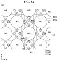
- FIG. 3A is a view illustrating one example of the pixels and the light transmitting parts of the sensing region CA.
- FIG. 3B is a view illustrating another example of the pixels and the light transmitting parts of the sensing region CA. Lines connected to the pixels are omitted in FIGS. 2 , 3A and 3B .
- the display region DA includes pixels PIX1 and PIX2 arranged in a matrix form.
- Each of the pixels PIX1 and PIX2 may be implemented as a real type pixel in which R, G, and B sub-pixels of three primary colors are configured as one pixel.
- Each of the pixels PIX1 and PIX2 may further include a W sub-pixel omitted from the drawing.
- two sub-pixels may be configured as one pixel using a sub-pixel rendering algorithm.
- a first pixel PIX1 may be composed of the R and G sub-pixels
- a second pixel PIX2 may be composed of the B and G sub-pixels.
- Insufficient color representation in each of the pixels PIX1 and PIX2 may be compensated by an average value of corresponding color data between neighboring pixels.
- the sensing region CA includes pixel groups PG spaced apart from each other by a predetermined pitch, and light transmitting parts AG disposed between neighboring pixel groups PG. External light is received by the lens of the sensing element module (in this case, the imaging element module) through the light transmitting parts AG.
- the light transmitting parts AG may include transparent media having high transmittance without metal so that the light may be incident with minimal light loss. In other words, the light transmitting parts AG may be formed of transparent insulating materials without including metal lines or pixels.
- the transmittance of the sensing region CA increases as the light transmitting parts AG increase.
- the pixel group PG may include one or two pixels. Each of the pixels of the pixel group may include two to four sub-pixels. For example, one pixel in the pixel group may include R, G, and B sub-pixels or may include two sub-pixels, and may further include a W sub-pixel.
- the first pixel PIX1 is composed of the R and G sub-pixels
- the second pixel PIX2 is composed of the B and G sub-pixels, but the present disclosure is not limited thereto.
- a distance D3 between the light transmitting parts AG is smaller than a pitch D1 between the pixel groups PG.
- a pitch D2 between the sub-pixels is smaller than the pitch D1 between the pixel groups PG.
- FIG. 3B shows another example of the pixels and the light transmitting parts of the sensing region CA.
- the structure of the another example as shown in FIG. 3B can be similar to that of the example as shown in FIG. 3A , except for the size of the light transmitting parts AG.
- each of the light transmitting parts AG as shown in FIG. 3B is enlarged compared to the example as shown in FIG. 3A , and it is clear from FIG. 3B that the distance D3 between the light transmitting parts AG is smaller than the pitch D2 between the sub-pixels (that is, D3 ⁇ D2). As a result, the light transmitting parts AG can be maximized and the transmittance in the sensing region CA can be improved.
- each of the light transmitting parts AG is exemplified as a circular shape in FIG. 3A and 3B , but is not limited thereto.
- each of the light transmitting parts AG may be designed in various shapes such as a circular shape, an oval shape, a polygonal shape, and the like.
- the light transmitting parts AG may be defined as regions from which all metal layers are removed in the screen.
- metal used as a cathode may be uniformly deposited on an entire screen, and then a cathode layer may be removed only in the light transmitting parts of the sensing region CA in the laser ablation process.
- the cathode layer may be melted and removed while irradiating a laser beam with a point shot and moving the laser beam along X-axis and Y-axis directions.
- the wavelength of the laser beam applied in the laser ablation process is selected as a wavelength having a high absorption coefficient of the cathode material.
- a diameter of a beam spot (BSPOT) of the beam formed on the cathode layer should be smaller than the light transmitting part AG as shown in FIG. 4 .
- BSPOT beam spot
- process time increases, and a undesired residual metal CR of the cathode layer not exposed to the beam spot may remain on the light transmitting part AG.
- a margin between the display region DA and the sensing region CA should be sufficiently secured so that cathodes of the pixels are not removed at a boundary between the display region DA and the sensing region CA.
- a light shield layer which exposes a light transmitting part region is formed in the screen of the display panel 100, and in the laser ablation process, the laser beam is irradiated in the shape of a line beam or block beam.
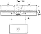
- FIG. 6A is a view illustrating a schematic cross-sectional structure of the display panel 100 according to one embodiment of the present disclosure and the laser beam irradiated in the laser ablation process.
- FIG. 6B is a view illustrating a schematic cross-sectional structure of the display panel according to another embodiment of the present disclosure and the laser beam irradiated in the laser ablation process.
- the display panel 100 includes a light shield layer LS which blocks the laser beam, and a metal layer ML exposed to the laser beam through an opening hole OP from which the light shield layer LS is removed.
- the light shield layer LS may be deposited in the entire display region DA and the entire sensing region CA, and then is patterned in a photolithography process.
- the light shield layer LS may be formed in the entire display region DA and the entire sensing region CA, or in at least the pixel region in the display region DA and the sensing region CA, and is removed from an opening hole region which exposes the light transmitting part AG of the sensing region CA to define the opening hole OP.
- the light shield layer LS may be formed only in the sensing region CA, and is removed from an opening hole region which exposes the light transmitting part AG of the sensing region CA to define the opening hole OP.
- the pixel region refers to a region where the pixels PIX1 and PIX2 are disposed in each of the display region DA and the sensing region CA.
- the metal layer ML is one of the metal layers required to drive the pixels of the display panel 100, and is a metal layer which should be removed from the light transmitting part AG of the sensing region CA.
- the metal layer ML may be a cathode material layer or a metal layer formed on a layer other than the cathode material layer.
- a wavelength of a laser beam LB is determined in a wavelength band in which an absorption coefficient of this metal is high.
- the light shield layer LS should protect the metal layer ML which is present in the screen other than the light transmitting part AG of the sensing region CA from the laser beam LB generated in the laser ablation process.
- the light shield layer LS should be selected from a material having a low absorption coefficient at a wavelength of the laser beam LB.
- the metal layer ML is a Mg/Ag alloy thin film layer used as a cathode material
- Mg has a high absorption coefficient at a wavelength of 1,064 nm.
- amorphous silicon (a-Si) or molybdenum (Mo) has a low absorption coefficient at the wavelength of 1,064 nm.
- the light shield layer LS for protecting the Mg/Ag thin film alloy layer from the laser beam in a region other than the light transmitting part includes a material with a low absorption coefficient at the wavelength of 1,064 nm, such as amorphous silicon (a-Si), molybdenum (Mo), or the like.
- a-Si amorphous silicon
- Mo molybdenum
- the laser beam LB may be irradiated in the shape of the line beam or block beam in the laser ablation process.
- a length of the line beam or block beam may be greater than that of the sensing region CA.
- a length of a beam spot BSPOT of the laser beam LB irradiated to the display panel 100 in the shape of the line beam or block beam may be at least a length greater than or equal to the length of the sensing region CA in one direction (X-axis or Y-axis direction).
- the beam spot BSPOT When the beam spot BSPOT is irradiated greater than the sensing region CA, only a part of the metal layer ML in the light transmitting part region exposed from the opening hole OP without the light shield layer LS may be exposed to the laser beam, and the metal layer ML in another region shielded by the light shield layer LS may be protected from the laser beam.
- a laser ablation apparatus may generate a line-shaped or block-shaped beam having a uniform laser beam intensity using a beam shaper or homogenizer (BSH).
- a line beam or a block beam may be generated according to a structure of the beam shaper BSH, and a size of the laser beam LB may be adjusted according to a distance between the beam shaper BSH and the substrate of the display panel 100.
- the metal layer ML may be completely removed at the same time from the light transmitting parts AG in the sensing region CA.
- the metal layer ML present in a pixel array other than the light transmitting parts AG is protected from the laser beam LB by the light shield layer LS, and thus is not removed in the laser ablation process.
- the metal layer ML may be removed only from the light transmitting parts of the sensing region CA within the screen by only irradiating the laser beam once. Accordingly, in the present disclosure, the laser ablation process time may be minimized and the margin between the display region DA and the sensing region CA may be minimized. Further, in the present disclosure, the transmittance of the sensing region CA may be increased, and the noise of the imaged image data may be reduced by completely removing the metal layer ML without the residual metal from the light transmitting parts AG.
- FIGS. 7 to 9 are views illustrating various laser beam spots, which are especially suitable to be used in a laser ablation process for manufacturing the display panel as shown in FIG. 6A , according to one embodiment of the present disclosure.
- the laser beam LB is irradiated in a shape of a line beam which crosses the sensing region CA. Since only the metal layer ML exposed to the laser beam LB is removed through the opening hole OP without the light shield layer LS, the length of the laser beam LB may be sufficiently long.
- a width Wb of the laser beam LB may be greater than a diameter R or maximum length of the light transmitting part AG, and further, may be greater than or equal to a diameter or maximum length of the sensing region CA.
- a length L of the laser beam LB may be greater than or equal to the maximum length of the sensing region CA.
- the laser beam LB irradiated to the display panel 100 in the shape of a line beam scans the display panel 100 while moving along a first direction (X or Y axis direction).
- the laser beam LB has a large beam spot, and thus may be irradiated to not only the sensing region CA, but also a part of the display region DA close to the sensing region CA, or an entire surface of the display region DA. At least a part of the laser beam may overlap between a previous shot and a current shot so that the metal residual metal does not remain in the light transmitting part AG of the sensing region CA while the laser beam LB moves along the first direction.
- the laser beam LB may scan the display panel 100 along the first direction (X or Y axis direction) and then scan the display panel 100 along a second direction (X or Y axis direction) to surely remove the residual metal by removing the metal layer ML only in the light transmitting part region. Since the metal layer ML is a thin film, generally, the metal layer ML may be removed without the residual metal only by laser scanning in one direction.
- the laser beam LB may be irradiated as a block beam having a size greater than or equal to the light transmitting part AG, and further, greater than or equal to the sensing region CA. Accordingly, since the beam spot of the laser beam LB irradiated in the shape of the block beam is large, the laser beam LB is irradiated to the entire surface of the light transmitting part AG in one shot, and further, may be irradiated to the entire surface of the sensing region CA in one shot.
- the beam spot of the block beam covers the entire surface of the sensing region CA, a metal layer selected from all the light transmitting parts AG of the sensing region CA, for example, the cathode may be removed by irradiation of the one-shot laser beam.
- the shape, the size, and the like of the block beam are determined by the beam shaper (BSH), and the intensity of the laser beam is constant within a block.
- the block beam may be a circular beam or a quadrangular beam, but the shape is not limited to a specific shape.
- the size of the laser beam LB may be sufficiently large.
- the block-shaped laser beam formed on the display panel 100 may be irradiated to not only the sensing region CA, but also a part of the display region DA close to the sensing region CA, or the entire surface of the display region DA in one shot. Accordingly, the metal layer ML of all light transmitting parts AG may be simultaneously removed from the screen without the residual metal with only one shot of the laser beam LB.
- numerous display panels 100 may be simultaneously manufactured through a multi-faceted process.
- a process of forming a thin film on a plurality of cells CELL on a mother substrate MSUBS is simultaneously performed.
- one cell is a single unit of the display panel 100.
- Circuit layers 12 of the cells CELL are simultaneously formed on the mother substrate MSUBS.
- the circuit layer 12 includes the light shield layer LS which exposes the light transmitting part region. When removing the metal layer in the circuit layer 12 formed in the light transmitting part region from the circuit layer 12, the laser ablation process may be performed.
- the mother substrate MSUBS is cut by a scribing wheel along a scribing line in a scribing process, and thus is separated in units of cells.
- a contour of each of the display panels 100 is trimmed by laser cutting equipment.
- the laser beam LB in the shape of the line beam or block beam may be irradiated to the mother substrate MSUBS.
- the size of the beam spot may be larger than that of the light transmitting part AG of the sensing region CA, and may have a size capable of completely covering the sensing region CA or a larger size capable of covering the unit cell CELL.
- FIG. 10 is a photographic image illustrating an experimental result in which the metal layer is removed from the light transmitting part region after performing the laser ablation process according to one embodiment of the present disclosure.
- the metal layer ML may be cleanly removed from the light transmitting parts AG of the sensing region CA to which the laser beam is irradiated as shown in FIGS. 6A to 9 without the residual metal.
- FIG. 11 is a block diagram illustrating the display panel and a display panel driving part according to one embodiment of the present disclosure.
- FIG. 12 is a block diagram schematically illustrating a configuration of a drive IC.
- a display device includes the display panel 100 in which the pixel array is disposed on the screen, the display panel driving part, and the like.
- the pixel array of the display panel 100 includes data lines DL, gate lines GL which intersect the data lines DL, and pixels P arranged in a matrix form defined by the data lines DL and the gate lines GL.
- the pixel array further includes power lines such as a VDD line PL1, a Vini line PL2, and a VSS line PL3 shown in FIGS. 13 and 14 .
- the pixel array may be divided into the circuit layer 12 and a light emitting element layer 14 as shown in FIG. 1 .
- a touch sensor array may be disposed on the light emitting element layer 14.
- each of the pixels of the pixel array may include two to four sub-pixels.
- Each of the sub-pixels includes a pixel circuit disposed on the circuit layer 12.
- a screen on which an input image is reproduced on the display panel 100 includes the display region DA and the sensing region CA.
- the sub-pixels of each of the display region DA and the sensing region CA include the pixel circuit.
- the pixel circuit may include a driving element which supplies a current to a light emitting element (OLED), a plurality of switch elements which sample a threshold voltage of the driving element and switch a current path of the pixel circuit, a capacitor which maintains a gate voltage of the driving element, and the like.
- the pixel circuit is disposed under the light emitting element.
- the sensing region CA includes the light transmitting parts AG disposed between the pixel groups, and an imaging element module (for example, a camera) 400 disposed under the sensing region CA.
- the imaging element module 400 photoelectrically converts light incident through the sensing region CA in an imaging mode using an image sensor, converts pixel data of the image output from the image sensor to digital data, and then outputs the imaged image data.
- the display panel driving part writes the pixel data of the input image to the pixels P.
- the pixels P may be interpreted as pixel groups including a plurality of sub-pixels.
- the display panel driving part includes a data driving part 306 which supplies a data voltage of the pixel data to the data lines DL, and a gate driving part 120 which sequentially supplies a gate pulse to the gate lines GL.
- the data driving part 306 may be integrated in a drive integrated circuit (IC) 300.
- the display panel driving part may further include a touch sensor driving part omitted in the drawing.
- the drive IC 300 may be adhered to the display panel 100.
- the drive IC 300 receives the pixel data of the input image and a timing signal from a host system 200 to supply the data voltage of the pixel data to the pixels, and synchronizes the data driving part 306 and the gate driving part 120.
- the drive IC 300 is connected to the data lines DL through data output channels to supply the data voltage of the pixel data to the data lines DL.
- the drive IC 300 may output a gate timing signal for controlling the gate driving part 120 through gate timing signal output channels.
- the gate timing signal generated from a timing controller 303 may include a gate start pulse VST, a gate shift clock CLK, and the like.
- the gate start pulse VST and the gate shift clock CLK swing between a gate-on voltage VGL and a gate-off voltage VGH.
- the gate timing signals VST and CLK output from a level shifter 307 are applied to the gate driving part 120 to control a shift operation of the gate driving part 120.
- the gate driving part 120 may include a shift register formed on the circuit layer of the display panel 100 together with the pixel array.
- the shift register of the gate driving part 120 sequentially supplies a gate signal to the gate lines GL under control of the timing controller 303.
- the gate signal may include a scan pulse and an EM pulse of a light emission signal.
- the shift register may include a scan driving part which outputs the scan pulse and an EM driving part which outputs the EM pulse.
- GVST and GCLK are gate timing signals input to the scan driving part.
- EVST and ECLK are gate timing signals input to the EM driving part.
- the drive IC 300 may be connected to the host system 200, a first memory 301, and the display panel 100.
- the drive IC 300 may include a data receiving and calculating part 308, the timing controller 303, the data driving part 306, a gamma compensation voltage generator 305, a power supply part 304, a second memory 302, and the like.
- the data receiving and calculating part 308 includes a receiving part receiving the pixel data input as digital signals from the host system 200 and a data calculating part which processes the pixel data input through the receiving part to improve image quality.
- the data calculating part may include a data restoration part which decodes and restores compressed pixel data, and an optical compensation part which adds a predetermined optical compensation value to the pixel data.
- the optical compensation value may be set as a value for correcting luminance of each piece of pixel data based on luminance of the screen measured based on the camera image taken in the fabricating process.
- the timing controller 303 provides the pixel data of the input image received from the host system 200 to the data driving part 306.
- the timing controller 303 generates a gate timing signal for controlling the gate driving part 120 and a source timing signal for controlling the data driving part 306 to control operation timings of the gate driving part 120 and the data driving part 306.
- the data driving part 306 converts the digital data including the pixel data received from the timing controller 303 through a digital to analog converter (DAC) to a gamma compensation voltage to output the data voltage.
- the data voltage output from the data driving part 306 is supplied to the data lines DL of the pixel array through an output buffer connected to a data channel of the drive IC 300.
- the gamma compensation voltage generator 305 divides a gamma reference voltage from the power supply part 304 through a divider circuit to generate a gamma compensation voltage for each gray level.
- the gamma compensation voltage is an analog voltage in which a voltage is set for each gray level of pixel data.
- the gamma compensation voltage output from the gamma compensation voltage generator 305 is provided to the data driving part 306.
- the power supply part 304 generates the power required for driving the pixel array of the display panel 100, the gate driving part 120, and the drive IC 300 using a DC-DC converter.
- the DC-DC converter may include a charge pump, a regulator, a buck converter, a boost converter, and the like.
- the power supply part 304 may adjust a DC input voltage from the host system 200 to generate DC power such as the gamma reference voltage, the gate-on voltage VGL, a gate-off voltage VGH, a pixel driving voltage VDD, a low potential power voltage VSS, and an initialization voltage Vini.
- the gamma reference voltage is supplied to the gamma compensation voltage generator 305.
- the gate-on voltage VGL and the gate-off voltage VGH are supplied to the level shifter 307 and the gate driving part 120.
- the pixel power such as the pixel driving voltage VDD, the low potential power voltage VSS, the initialization voltage Vini, and the like are commonly supplied to the pixels P.
- the initialization voltage Vini is set to a DC voltage lower than the pixel driving voltage VDD and lower than the threshold voltage of the light emitting element (OLED) to initialize main nodes of the pixel circuits and restrain light emission of the light emitting element (OLED).
- the second memory 302 stores a compensation value, register setting data, and the like received from the first memory 301 when power is supplied to the drive IC 300.
- the compensation value may be applied to various algorithms to improve image quality.
- the compensation value may include the optical compensation value.
- the register setting data defines operations of the data driving part 306, the timing controller 303, the gamma compensation voltage generator 305, and the like.
- the first memory 301 may include a flash memory.
- the second memory 302 may include a static random-access memory (SRAM).
- the host system 200 may be implemented as an application processor (AP).
- the host system 200 may transmit the pixel data of the input image to the drive IC 300 through a mobile industry processor interface (MIPI).
- MIPI mobile industry processor interface
- the host system 200 may be connected to the drive IC 300 through a printed circuit, for example, a flexible printed circuit (FPC).
- FPC flexible printed circuit
- the display panel 100 may be implemented as a flexible panel applicable to a flexible display.
- the flexible display may be changed in screen size by rolling, folding, and bending the flexible panel, and may be easily fabricated in various designs.
- the flexible display may be implemented as a rollable display, a foldable display, a bendable display, a slidable display, or the like.
- the flexible panel may be fabricated as a so-called "plastic OLED panel".
- the plastic OLED panel may include a back plate and a pixel array on an organic thin film bonded to the back plate.
- a touch sensor array may be formed on the pixel array.
- the back plate may be a polyethylene terephthalate (PET) substrate.
- the pixel array and the touch sensor array may be formed on the organic thin film.
- the back plate may block moisture permeation toward the organic thin film so that the pixel array is not exposed to moisture.
- the organic thin film may be a polyimide (PI) substrate.
- a multi-layered buffer film made of an insulating material (not shown) may be formed on the organic thin film.
- the circuit layer 12 and the light emitting element layer 14 may be stacked on the organic thin film.
- the pixel circuit, the gate driving part, and the like disposed on the circuit layer 12 may include a plurality of transistors.
- the transistors may be implemented as an oxide thin film transistors (TFTs) including an oxide semiconductor, LTPS TFTs including low temperature polysilicon (LTPS), or the like.
- TFTs oxide thin film transistors
- LTPS TFTs including low temperature polysilicon
- Each of the transistors may be implemented as a p-channel TFT or an n-channel TFT.
- LTPS low temperature polysilicon
- the transistor is a three-electrode element including a gate, a source, and a drain.
- the source is an electrode which supplies carriers to the transistor. In the transistor, the carriers start flowing from the source.
- the drain is an electrode through which the carriers exit from the transistor. In the transistor, the carriers flow from the source to the drain.
- a source voltage is lower than a drain voltage so that the electrons may flow from the source to the drain.
- the p-channel transistor since the carriers are holes, a source voltage is higher than a drain voltage so that the holes may flow from the source to the drain.
- the source and drain of the transistor are not fixed.
- the source and drain may be changed according to the applied voltage. Accordingly, the disclosure is not limited due to the source and drain of the transistor.
- the source and drain of the transistor will be referred to as first and second electrodes.
- the gate pulse swings between the gate-on voltage and the gate-off voltage.
- the gate-on voltage is set to a voltage higher than the threshold voltage of the transistor, and the gate-off voltage is set to a voltage lower than the threshold voltage of the transistor.
- the transistor is turned on in response to the gate-on voltage, but is turned off in response to the gate-off voltage.
- the gate-on voltage may be a gate high voltage VGH and the gate-off voltage may be a gate low voltage VGL.
- the gate-on voltage may be the gate low voltage VGL
- the gate-off voltage may be the gate high voltage VGH.
- the driving element of the pixel circuit may be implemented as a transistor.
- the driving element should have uniform electrical characteristics among all pixels, but due to process variations and element characteristic variations, there may be differences between pixels and the electrical characteristics may be changed according to the elapse of a display driving time.
- the display device may include an internal compensation circuit and an external compensation circuit.
- the internal compensation circuit samples a threshold voltage (Vth) and/or mobility ( ⁇ ) of the driving element, which is added to the pixel circuit in each of the sub-pixels and changes according to the electrical characteristics of the driving element, and compensates for the change in real time.
- the external compensation circuit transmits a threshold voltage and/or mobility of the driving element sensed through a sensing line connected to each of the sub-pixels to an external compensation part.
- the compensation part of the external compensation circuit compensates for changes of the electrical characteristics of the driving element by reflecting a sensing result and modulating the pixel data of the input image. Since the voltage of the pixel which is changed according to the electrical characteristics of an external compensation driving element is sensed, and the external circuit modulates the data of the input image based on the sensed voltage, the electrical characteristic variation of the driving element between the pixels is compensated for.
- FIGS. 13 and 14 are circuit diagrams illustrating one example of the pixel circuit to which the internal compensation circuit is applied.
- FIG. 15 is a view illustrating a method of driving the pixel circuit shown in FIGS. 13 and 14 .
- the pixel circuit of the present disclosure is not limited to FIGS. 13 and 14 .
- the pixel circuits shown in FIGS. 13 and 14 may be equally applied to the pixel circuits of the display region DA and the sensing region CA.
- the pixel circuit applicable to the present disclosure may be implemented as the circuit shown in FIGS. 13 and 14 , but is not limited thereto.
- the pixel circuit includes a light emitting element OLED, a driving element DT which supplies a current to the light emitting element OLED, and an internal compensation circuit which compensates a gate voltage of the driving element DT as much as a threshold voltage Vth of the driving element DT by sampling the threshold voltage Vth of the driving element DT using a plurality of switch elements M1 to M6.
- Each of the driving element DT and the switch elements M1 to M6 may be implemented as a p-channel TFT.
- a driving period of the pixel circuit using the internal compensation circuit may be divided into an initialization period Tini, a sampling period Tsam, a data writing period Twr, and a light emission period Tem as shown in FIG. 15 .
- an N-1th scan signal SCAN(N-1) is generated as a pulse of a gate-on voltage VGL, and a voltage of each of an Nth scan signal SCAN(N) and a light emission signal EM(N) is a gate-off voltage VGH.
- the Nth scan signal SCAN(N) is generated as a pulse of the gate-on voltage VGL, and a voltage of each of the N-1th scan signal SCAN(N-1) and the light emission signal EM(N) is the gate-off voltage VGH.
- the voltage of each of the N-1th scan signal SCAN(N-1), the Nth scan signal SCAN(N), and the light emission signal EM(N) is the gate-off voltage VGH.
- the light emission signal EM(N) is generated as the gate-on voltage VGL, and the voltage of each of the N-1th scan signal SCAN(N-1) and the Nth scan signal SCAN (N) is generated as the gate-off voltage VGH.
- a fifth switch element M5 is turned on according to the gate-on voltage VGL of the N-1th scan signal SCAN(N-1) to initialize the pixel circuit.
- a threshold voltage of the driving element DT is sampled and stored in a capacitor Cst1.
- a sixth switch element M6 is turned on during the sampling period Tsam to lower the voltage of a fourth node n4 to a reference voltage Vref to restrain the light emission of the light emitting element OLED.
- the first to sixth switch elements M1 to M6 maintain an off state.
- the third and fourth switch elements M3 and M4 are turned on so that the light emitting element OLED emits light.
- the light emission signal EM(N) swings at a predetermined duty ratio between the gate-on low voltage VGL and the gate-off voltage VGH, and thus the third and fourth switch elements M3 and M4 may be repeatedly turned on/off.
- the light emitting element OLED may be implemented as an organic light emitting diode or an inorganic light emitting diode.
- an example in which the light emitting element OLED is implemented as an organic light emitting diode will be described.
- the light emitting element OLED may include an organic compound layer formed between an anode and a cathode.
- the organic compound layer may include a hole injection layer HIL, a hole transport layer HTL, a light emitting layer EML, an electron transport layer ETL, and an electron injection layer EIL, but is not limited thereto.
- the anode of the light emitting element OLED is connected to the fourth node n4 between the fourth and sixth switch elements M4 and M6.
- the fourth node n4 is connected to the anode of the light emitting element OLED, a second electrode of the fourth switch element M4, and a second electrode of the sixth switch element M6.
- the cathode of the light-emitting element OLED is connected to the VSS line PL3 to which the low potential power supply voltage VSS is applied.
- the light emitting element OLED emits light with a current Ids flowing according to a gate-source voltage Vgs of the driving element DT. A current path of the light emitting element OLED is switched by the third and fourth switch elements M3 and M4.
- the storage capacitor Cst1 is connected between the VDD line PL1 and a first node n1.
- the data voltage Vdata compensated by the threshold voltage Vth of the driving element DT is charged in the storage capacitor Cst1. Since the data voltage Vdata in each of the sub-pixels is compensated as much as the threshold voltage Vth of the driving element DT, the characteristic variation of the driving element DT is compensated for in the sub-pixels.
- the first switch element M1 is turned on in response to the gate-on voltage VGL of the Nth scan pulse SCAN(N) to connect a second node n2 and a third node n3.
- the second node n2 is connected to a gate electrode of the driving element DT, a first electrode of the storage capacitor Cst1, and a first electrode of the first switch element M1.
- the third node n3 is connected to a second electrode of the driving element DT, a second electrode of the first switch element M1, and a first electrode of the fourth switch element M4.
- a gate electrode of the first switch element M1 is connected to the first gate line GL1 to receive the Nth scan pulse SCAN(N).
- the first electrode of the first switch element M1 is connected to the second node n2, and the second electrode of the first switch element M1 is connected to the third node n3.
- the first switch element M1 Since the first switch element M1 is turned on only one very short horizontal period (1H) in which the Nth scan signal SCAN(N) is generated as the gate-on voltage VGL in one frame period and thus it is maintained in an off state for approximately one frame period, a leakage current may occur in the off state of the first switch element M1.
- the first switch element M1 may be implemented as a transistor having a dual gate structure in which two transistors M1a and M1b are connected in series as shown in FIG. 14 .
- the second switch element M2 is turned on in response to the gate-on voltage VGL of the Nth scan pulse SCAN(N) to supply the data voltage Vdata to the first node n1.
- a gate electrode of the second switch element M2 is connected to the first gate line GL1 to receive the Nth scan pulse SCAN(N).
- a first electrode of the second switch element M2 is connected to the first node n1.
- a second electrode of the second switch element M2 is connected to the data lines DL to which the data voltage Vdata is applied.
- the first node n1 is connected to the first electrode of the second switch element M2, a second electrode of the third switch element M3, and a first electrode of the driving element DT.
- the third switch element M3 is turned on in response to the gate-on voltage VGL of the light emission signal EM(N) to connect the VDD line PL1 to the first node n1.
- a gate electrode of the third switch element M3 is connected to a third gate line GL3 to receive the light emission signal EM(N).
- a first electrode of the third switch element M3 is connected to the VDD line PL1.
- the second electrode of the third switch element M3 is connected to the first node n1.
- the fourth switch element M4 is turned on in response to the gate-on voltage VGL of the light emission signal EM(N) to connect the third node n3 to the anode of the light emitting element OLED.
- a gate electrode of the fourth switch element M4 is connected to the third gate line GL3 to receive the light emission signal EM(N).
- the first electrode of the fourth switch element M4 is connected to the third node n3, and the second electrode of the fourth switch element M4 is connected to the fourth node n4.
- the fifth switch element M5 is turned on in response to the gate-on voltage VGL of the N-1th scan pulse SCAN(N-1) to connect the second node n2 to the Vini line PL2.
- a gate electrode of the fifth switch element M5 is connected to a second gate line GL2 to receive the N-1th scan pulse SCAN(N-1).
- a first electrode of the fifth switch element M5 is connected to the second node n2, and a second electrode of the fifth switch element M5 is connected to the Vini line PL2.
- the fifth switch element M5 is implemented as a transistor having a dual gate structure in which two transistors M5a and M5b are connected in series as shown in FIG. 14 .
- the sixth switch element M6 is turned on in response to the gate-on voltage VGL of the Nth scan pulse SCAN(N) to connect the Vini line PL2 to the fourth node n4.
- a gate electrode of the sixth switch element M6 is connected to the first gate line GL1 to receive the Nth scan pulse SCAN(N).
- a first electrode of the sixth switch element M6 is connected to the Vini line PL2, and the second electrode of the sixth switch element M6 is connected to the fourth node n4.
- the driving element DT drives the light emitting element OLED by controlling the current Ids flowing through the light emitting element OLED according to the gate-source voltage Vgs.
- the driving element DT includes a gate connected to the second node n2, a first electrode connected to the first node n1, and a second electrode connected to the third node n3.
- the N-1th scan pulse SCAN(N-1) is generated as the gate-on voltage VGL.
- the Nth scan pulse SCAN(N) and the light emission signal EM(N) maintain the gate-off voltage VGH during the initialization period Tini.
- the fifth switch element M5 is turned on during the initialization period Tini, the second and fourth nodes n2 and n4 are initialized to the initialization voltage Vini.
- a hold period Th may be set between the initialization period Tini and the sampling period Tsam. In the hold period Th, the gate pulses SCAN(N-1), SCAN(N), EM(N) maintain previous states.
- the Nth scan pulse SCAN(N) is generated as the gate-on voltage VGL.
- the pulse of the Nth scan pulse SCAN(N) is synchronized with the data voltage Vdata of an Nth pixel line.
- the N-1th scan pulse SCAN(N-1) and the light emission signal EM(N) maintain the gate-off voltage VGH during the sampling period Tsam. Accordingly, the first and second switch elements M1 and M2 are turned on during the sampling period Tsam.
- a gate voltage DTG of the driving element DT increases due to the current flowing through the first and second switch elements M1 and M2.
- the gate node voltage DTG is Vdata-
- the voltage of the first node n is also Vdata-
- the gate-source voltage Vgs of the driving element DT is
- Vdata -(Vdata-
- )
- the Nth scan pulse SCAN(N) is inverted to the gate-off voltage VGH.
- the N-1th scan pulse SCAN(N-1) and the light emission signal EM(N) maintain the gate-off voltage VGH during the data writing period Twr. Accordingly, all switch elements M1 to M6 maintain the off state during the data writing period Twr.
- the light emission signal EM(N) may be generated as the gate-on voltage VGL.
- the light emission signal EM(N) is turned on and off at a predetermined duty ratio to improve low gray scale expression, and thus may swing between the gate-on voltage VGL and the gate-off voltage VGH. Accordingly, the light emission signal EM(N) may be generated as the gate-on voltage VGL during at least some part of the light emission period Tem.
- the light emitting element OLED may emit light.
- the N-1th and Nth scan pulses SCAN(N-1) and SCAN(N) maintain the gate-off voltage VGH.
- the third and fourth switch elements M3 and M4 repeat on and off operations according to the voltage of the light emission signal EM.
- the light emission signal EM(N) is the gate-on voltage VGL, since the third and fourth switch elements M3 and M4 are turned on, a current flows through the light emitting element OLED.
- the gate-source voltage Vgs of the driving element DT is
- VDD-(Vdata-
- K is a constant value determined by charge mobility, a parasitic capacitance, a channel capacity of the driving element DT, and the like.
- FIG. 16 is a cross-sectional view illustrating the cross-sectional structure of the display panel according to one embodiment of the present disclosure in detail. It should be noted that the cross-sectional structure of the display panel 100 is not limited to FIG. 16 .
- TFT represents the driving element DT of the pixel circuit.
- the circuit layer 12, the light emitting element layer 14, and the like may be stacked on substrates PI1 and PI2.
- the substrates PI1 and PI2 may include first and second PI substrates PI1 and PI2.
- An inorganic film IPD may be formed between the first PI substrate PI1 and the second PI substrate PI2. The inorganic film IPD blocks moisture penetration.
- a first buffer layer BUF1 may be formed on the second PI substrate PI2. As shown in FIG. 21 , the first buffer layer BUF1 may be formed of a multi-layered insulating film in which two or more oxide films SiO 2 and nitride films SiN x are stacked. A first metal layer may be formed on the first buffer layer BUF1, and a second buffer layer BUF2 may be formed on the first metal layer. The first metal layer is patterned in the photolithography process. The first metal layer may include a bottom shield metal pattern BSM. The bottom shield metal pattern BSM blocks external light so that light is not irradiated to an active layer of the TFT and thus prevents a photocurrent of the TFT formed in the pixel region.
- the bottom shield metal pattern BSM When the bottom shield metal pattern BSM is formed of a metal having a lower absorption coefficient of the laser wavelength used in the laser ablation process compared to the metal layer ML which should be removed from the sensing region CA, the bottom shield metal pattern BSM may also serve as the light shield layer LS which blocks the laser beam LB in the laser ablation process.
- Each of the first and second buffer layers BUF1 and BUF2 may be formed of an inorganic insulating material and may be formed of one or more insulating layers.
- An active layer ACT is formed of a semiconductor material deposited on the second buffer layer BUF2 and may be patterned by a photolithography process.
- the active layer ACT includes an active pattern of each of the TFTs of the pixel circuit and the TFTs of the gate driving part.
- a portion of the active layer ACT may be metallized by ion doping. The metallized portion may be used as a jumper pattern which connects metal layers at some nodes of the pixel circuit to connect components of the pixel circuit.
- a gate insulating layer GI may be formed on the second buffer layer BUF2 to cover the active layer ACT.
- the gate insulating layer GI may be formed of an inorganic insulating material.
- a second metal layer may be formed on the gate insulating layer GI.
- the second metal layer may be patterned by a photolithography process.
- the second metal layer may include gate lines and a gate electrode pattern GATE, a lower electrode of the storage capacitor Cst1, a jumper pattern which connects patterns of the first metal layer and a third metal layer, and the like.
- a first interlayer insulating layer ILD1 may be formed on the gate insulating layer GI to cover the second metal layer.
- the third metal layer may be formed on the first interlayer insulating layer ILD1, and a second interlayer insulating layer ILD2 may cover the third metal layer.
- the third metal layer may be patterned by a photolithography process.
- the third metal layer may include metal patterns TM such as an upper electrode of the storage capacitor Cst1.
- the first and second interlayer insulating layers ILD1 and ILD2 may include an inorganic insulating material.
- a fourth metal layer may be formed on the second interlayer insulating layer ILD2, and an inorganic insulating layer PAS1 and a first planarization layer PLN1 may be stacked thereon.
- a fifth metal layer may be formed on the first planarization layer PLN1.
- Some patterns of the fourth metal layer may be connected to the third metal layer through a contact hole passing through the first planarization layer PLN1 and the inorganic insulating layer PAS1.
- the first and second planarization layers PLN1 and PLN2 may be formed of an organic insulating material which flattens a surface.
- the fourth metal layer may include the first and second electrodes of the TFT connected to the active pattern of the TFT through a contact hole passing through the second interlayer insulating layer ILD2.
- the data lines DL and the power lines PL1, PL2, and PL3 may be implemented as a fourth metal layer pattern SD1 or a fifth metal layer pattern SD2.
- An anode AND of the light emitting element OLED may be formed on the second planarization layer PLN2.
- the anode AND may be connected to the electrodes of the TFT used as a switch element or a driving element through a contact hole passing through the second planarization layer PLN2.
- the anode AND may be formed of a transparent or translucent electrode material.
- a pixel definition film BNK may cover the anode AND of the light emitting element OLED.
- the pixel definition film BNK is formed in a pattern which defines a light emitting region (or an opening region) through which light passes from each of the pixels to the outside.
- a spacer SPC may be formed on the pixel definition film BNK The pixel definition film BNK and the spacer SPC may be integrated with the same organic insulating material. The spacer SPC secures a gap between a fine metal mask (FMM) and the anode AND so that the FMM does not come into contact with the anode AND in a deposition process of an organic compound EL.
- FMM fine metal mask
- the organic compound EL is formed in the light emitting region of each of the pixels defined by the pixel definition film BNK
- a cathode CAT of the light emitting element OLED is formed on the entire surface of the display panel 100 to cover the pixel definition film BNK, the spacer SPC, and the organic compound EL.
- the cathode CAT may be connected to the VSS line PL3 formed by any one of the metal layers thereunder.
- a capping layer CPL may cover the cathode CAT.
- the capping layer CPL blocks penetration of out gassing of the organic insulating material applied on the capping layer CPL and air by being formed of an inorganic insulating material on the cathode CAT to protect the cathode CAT.
- An inorganic insulating layer PAS2 may cover the capping layer CPL, and a planarization layer PCL may be formed on the inorganic insulating layer PAS2.
- the planarization layer PCL may include an organic insulating material.
- An inorganic insulating layer PAS3 of the encapsulation layer may be formed on the planarization layer PCL.
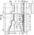
- FIGS. 17 and 18 are cross-sectional views illustrating the light shield layer LS of the pixel region and the light transmitting part AG of the sensing region CA in the cross-sectional structure of the display panel according to various embodiments of the present disclosure.
- components that are substantially the same as those shown in FIG. 16 are denoted by the same reference numerals, and detailed descriptions thereof will be omitted.
- the light shield layer LS protects pixel regions PIX of the display region DA and the sensing region CA from the laser beam LB irradiated to the display panel 100 in the laser ablation process.
- the light shield layer LS is removed from the region of the light transmitting part AG to define an opening hole OP which exposes the light transmitting part AG to the laser beam.
- the laser beam LB generated in the laser ablation process removes a metal layer to be removed through the opening hole OP of the light shield layer LS, for example, a cathode metal in the light transmitting part region.
- Each of the display region DA and the pixel region (the second pixel region) of the sensing region CA includes a light shield layer, and a metal layer having a higher absorption coefficient than the light shield layer for a specific wavelength of a laser beam.
- the metal layer of the cathode CAT may include magnesium (Mg).
- the light shield layer LS may be disposed under the TFT in the pixel region to prevent a photocurrent of the TFT.
- the light shield layer LS may be formed of metal having a lower absorption coefficient for the wavelength of the laser beam than the metal layer to be removed.
- the metal layer to be removed is a cathode material formed of an Mg/Ag alloy
- the light shield layer LS may be formed of Mo having an absorption coefficient lower than that of Mg for the laser beam LB having a wavelength of 1,064 nm. Mo is a metal having high light reflectance, and thus may prevent the photocurrent of the TFT by reflecting external light.
- the light shield layer LS shown in FIG. 17 is disposed between the inorganic insulating layers BUF1 and BUF2 under the TFT in the pixel region PIX.
- the light shield layer LS shown in FIG. 18 is an example formed of amorphous silicon (a-Si). Since the amorphous silicon has an absorption coefficient lower than that of Mg for the laser beam LB having the wavelength of 1,064 nm, upper metal layers may be protected from the laser beam for removing Mg and Ag in the laser ablation process. In this case, since the light shield layer LS may not block external light which affects the TFT of the pixel region PIX, a separate bottom shield metal pattern BSM may be added to the pixel region PIX.
- the bottom shield metal pattern BSM shown in FIG. 18 is disposed between the inorganic insulating layers BUF2 and BUF3 under the TFT in the pixel region PIX.
- the second buffer layer BUF2 is an inorganic insulating layer formed between the light shield layer LS and the bottom shield metal pattern BSM in the pixel region PIX.
- a third buffer layer BUF3 is an inorganic insulating layer formed between the light shield layer LS and the active layer ACT in the pixel region PIX.
- All metal layers in the pixel region PIX are removed from the light transmitting part AG. Accordingly, only transparent insulating layers may be present in the light transmitting part AG.
- One of the PI substrates PI1 and PI2 may be removed from the light transmitting part AG as shown in FIG. 19 .
- One or more of the inorganic insulating layers BUF1, BUF2, GI, ILD1, ILD2, and PAS1 may be removed from the light transmitting part AG, and one or more of the active layer ACT, the pixel definition film BNK, and the spacer SPC may be further removed. Due to the insulating layer(s) removed from the light transmitting part AG, a concave portion may be filled by the organic insulating layers PLN1 and PLN2.
- a difference in etch ratio may occur.
- the difference in etch ratio may cause size differences and the like of a gap and overlapping portion between the patterned metal patterns, and thus may cause a critical dimension (CD) defect.
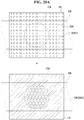
- a dummy pattern DPIX having the same pattern shape as the pixel region PIX may be formed on the metal layer ML of the light transmitting part AG as shown in FIG.
- the metal layer ML in the light transmitting part AG may be removed using the light shield layer LS in the laser ablation process as shown in FIG. 20B .
- the metal layer ML other than the opening hole OP of the light shield layer LS remains on the sensing region CA, and dummy patterns DP facing the opening hole OP of the light shield layer LS may be removed.
- the metal layer ML may be one or more of the first to fifth metal layers of the circuit layer 12.
- the light shield layer LS may be selected from a material having a lower absorption coefficient than that of the metal layer at the wavelength of the laser beam which removes the metal layer.
- a semiconductor layer ACT may be disposed over the light shield layer LS.
- the semiconductor layer ACT may be formed of amorphous silicon (a-Si).
- the amorphous silicon (a-Si) may be crystallized.
- the amorphous silicon (a-Si) of the semiconductor layer ACT may be crystallized in a laser crystallization (an excimer laser annealing (ELA)) process as shown in FIG. 21 .
- the amorphous silicon (a-Si) is converted to polysilicon having a polycrystalline structure by the laser crystallization process.
- an interlayer separation or film-delamination phenomenon may occur between the light shield layer LS and another layer adjacent thereto.
- the light shield layer LS is formed of the amorphous silicon (a-Si)
- hydrogen (H2) atoms may be bonded to a dangling bond of the amorphous silicon (a-Si).
- an amorphous silicon film used as the semiconductor layer ACT is scanned by a laser beam (a line beam) having a wavelength of 308 nm at a high temperature higher than or equal to a melting temperature of the amorphous silicon (a-Si), for example, 1,400°C or higher.
- the light shield layer LS may be sandwiched between materials having no hydrogen or a very low hydrogen content.
- a second oxide film OX2 is disposed between the semiconductor layer ACT and the light shield layer LS.
- a first oxide film OX1 may be disposed between the light shield layer LS and the first buffer layer BUF1 under the light shield layer LS.
- the light shield layer LS is formed between the first and second oxide films OX1 and OX2 without hydrogen atoms.
- the hydrogen atoms are not bonded to the amorphous silicon (a-Si) used as the light shield layer LS, it is possible to prevent the film-delamination phenomenon of the light shield layer LS in the laser crystallization process.
- the first and second oxide films OX1 and OX2 are exemplified as silicon oxide films SiO 2 in FIG. 21 , but are not limited thereto.
- each of the oxide films OX1 and OX2 may be formed as a single layer film or a multilayer film selected from the silicon oxide film (SiO 2 ), a zirconium oxide film (ZrO 2 ), and a hafnium oxide film (HfO 2 ).
- the first and second oxide films OX1 and OX2 may be formed of oxide films of the same material and may have the same thickness.
- the first and second oxide films OX1 and OX2 may be formed of oxide films of different materials or may be formed to have different thicknesses.
- a plurality of sensor modules may be disposed in the sensing region CA.
- an infrared sensor module omitted from the drawing may be further disposed together with the imaging element module 400 in the sensing region CA.
- Another sensor such as an illuminance sensor or a proximity sensor may be additionally disposed in the sensing region CA.
- Low PPI pixels and the light transmitting part AG may be disposed over light receiving surfaces 401 and 402 of the imaging element module 400 and the infrared sensor module, respectively.
- the number of and/or size of light transmitting parts AG may be small or the light transmitting parts AG may not be present in the light receiving surface 402 of the infrared sensor module compared to the light receiving surface 401 of the imaging element module. Meanwhile, the infrared sensor module may sense infrared rays and may be used for facial recognition.
- the light shield layer LS may be formed of a plurality of different materials by dividing regions within the sensing region CA. For example, when the infrared sensor module as well as the imaging element module are disposed on the sensing region CA as shown in FIG. 22A , the transparency of the light shield layer LS in a region where the infrared sensor module is located may be higher than the transparency of the light shield layer LS in a region where the imaging element module 400 is located. The transparency of the light shield layer LS may vary according to any electronic module located on the region where the light shield layer LS is located.
- amorphous silicon (a-Si) may be used as the light shield layer LS on the light receiving surface 402 of the infrared sensor module
- molybdenum Mo may be used as the light shield layer LS on the light receiving surface 401 of the imaging element module.
- FIG. 22B another example of the present disclosure is shown in FIG. 22B , in which only one sensor module (for example, a light sensor module other than an imaging element module) is disposed in the sensing region CA.
- the one sensor module comprises, but is not limited to, an infrared sensor module.
- a light shield layer having a low absorption coefficient for a specific laser wavelength is disposed in pixel regions other than a metal layer to be removed, light transmitting parts of an sensing region can be simultaneously removed by a large laser beam in a shape of a line beam or a block beam. Accordingly, in the present disclosure, the metal layer can be cleanly and quickly removed from the light transmitting parts without a residual metal, and fabrication costs of the display panel can be reduced by minimizing a laser ablation process time and a defect rate.
- the transmittance of the sensing region can be increased by completely removing the metal layer from the light transmitting parts without the residual metal, and a margin between a display region and the sensing region can be minimized.
- the metal layer is removed from the light transmitting parts without the residual metal, the transmittance of the sensing region can be increased, and the noise of imaged image data can be reduced.
Landscapes
- Engineering & Computer Science (AREA)
- Microelectronics & Electronic Packaging (AREA)
- Physics & Mathematics (AREA)
- Geometry (AREA)
- Manufacturing & Machinery (AREA)
- Chemical & Material Sciences (AREA)
- Inorganic Chemistry (AREA)
- Life Sciences & Earth Sciences (AREA)
- Sustainable Development (AREA)
- Electroluminescent Light Sources (AREA)
- Devices For Indicating Variable Information By Combining Individual Elements (AREA)
- Sewing Machines And Sewing (AREA)
Applications Claiming Priority (2)
| Application Number | Priority Date | Filing Date | Title |
|---|---|---|---|
| KR20200081557 | 2020-07-02 | ||
| KR1020200085531A KR102888214B1 (ko) | 2020-07-02 | 2020-07-10 | 표시패널과 그 제조 방법 |
Publications (1)
| Publication Number | Publication Date |
|---|---|
| EP3933931A1 true EP3933931A1 (de) | 2022-01-05 |
Family
ID=76623970
Family Applications (1)
| Application Number | Title | Priority Date | Filing Date |
|---|---|---|---|
| EP21181781.2A Pending EP3933931A1 (de) | 2020-07-02 | 2021-06-25 | Anzeigetafel und verfahren zur herstellung davon |
Country Status (5)
| Country | Link |
|---|---|
| US (3) | US11758776B2 (de) |
| EP (1) | EP3933931A1 (de) |
| KR (1) | KR20250167539A (de) |
| CN (2) | CN121335385A (de) |
| TW (1) | TWI811717B (de) |
Cited By (2)
| Publication number | Priority date | Publication date | Assignee | Title |
|---|---|---|---|---|
| EP4016634A1 (de) * | 2020-12-16 | 2022-06-22 | LG Display Co., Ltd. | Anzeigetafel und verfahren zur herstellung davon |
| DE102021123253B4 (de) | 2020-12-30 | 2025-10-23 | Lg Display Co., Ltd. | Anzeigepanel und Anzeigevorrichtung |
Families Citing this family (13)
| Publication number | Priority date | Publication date | Assignee | Title |
|---|---|---|---|---|
| CN116157763A (zh) * | 2020-07-21 | 2023-05-23 | 三星电子株式会社 | 包括显示器和相机装置的电子装置 |
| CN112382651B (zh) * | 2020-11-30 | 2025-05-23 | 京东方科技集团股份有限公司 | 显示面板及其制备方法、显示装置 |
| GB2610521A (en) * | 2021-01-04 | 2023-03-08 | Boe Technology Group Co Ltd | Display panel and manufacturing method therefor, and display apparatus |
| CN114497415B (zh) * | 2022-01-24 | 2024-03-19 | 京东方科技集团股份有限公司 | 显示面板及其制造方法、显示装置 |
| CN114927105B (zh) * | 2022-05-25 | 2024-12-27 | 四川芯辰光微纳科技有限公司 | 一种64阶灰度像素结构、显示介质 |
| CN117678341A (zh) * | 2022-06-24 | 2024-03-08 | 京东方科技集团股份有限公司 | 显示面板、显示装置及掩膜版 |
| CN115148933A (zh) * | 2022-06-30 | 2022-10-04 | 武汉天马微电子有限公司 | 一种显示面板及其制备方法、显示装置 |
| CN115148932B (zh) * | 2022-06-30 | 2025-12-02 | 湖北长江新型显示产业创新中心有限公司 | 显示面板及显示装置 |
| CN115347025B (zh) * | 2022-08-22 | 2025-08-05 | 京东方科技集团股份有限公司 | 一种显示面板、其制作方法及显示装置 |
| KR20240078532A (ko) * | 2022-11-25 | 2024-06-04 | 삼성디스플레이 주식회사 | 발광 표시 장치 |
| KR20240119763A (ko) * | 2023-01-30 | 2024-08-06 | 엘지디스플레이 주식회사 | 표시 패널 및 표시 장치 |
| CN116568061A (zh) * | 2023-03-14 | 2023-08-08 | 湖北长江新型显示产业创新中心有限公司 | 一种显示面板及其制备方法、显示装置 |
| CN116669460A (zh) * | 2023-05-05 | 2023-08-29 | 京东方科技集团股份有限公司 | 一种显示面板及其制备方法、显示装置 |
Citations (6)
| Publication number | Priority date | Publication date | Assignee | Title |
|---|---|---|---|---|
| KR20110071698A (ko) * | 2009-12-21 | 2011-06-29 | 삼성모바일디스플레이주식회사 | 평판 표시 장치 |
| US20120267611A1 (en) * | 2011-04-21 | 2012-10-25 | Jin-Koo Chung | Organic light-emitting display device |
| EP3032585A1 (de) * | 2014-12-11 | 2016-06-15 | Samsung Display Co., Ltd. | Anzeigetafel und organische lichtemittierende anzeigevorrichtung mit einer anzeigetafel |
| CN110764362A (zh) * | 2019-01-31 | 2020-02-07 | 昆山国显光电有限公司 | 掩膜条、阵列基板、显示屏及显示装置 |
| US20200066809A1 (en) * | 2017-09-30 | 2020-02-27 | Kunshan Go-Visionox Opto-Electronics Co., Ltd. | Display screen and display apparatus |
| US20200075680A1 (en) * | 2018-08-29 | 2020-03-05 | Chengdu Boe Optoelectronics Technology Co., Ltd. | Display panel and method for manufacturing the same |
Family Cites Families (17)
| Publication number | Priority date | Publication date | Assignee | Title |
|---|---|---|---|---|
| KR101227137B1 (ko) | 2006-03-27 | 2013-01-28 | 엘지디스플레이 주식회사 | 액정표시장치의 리페어 장치 및 이를 이용한 리페어 방법 |
| KR100785019B1 (ko) | 2006-06-09 | 2007-12-11 | 삼성전자주식회사 | 하부 게이트 박막 트랜지스터 및 그 제조방법 |
| JP2010153449A (ja) * | 2008-12-24 | 2010-07-08 | Seiko Epson Corp | 光源一体型光電変換装置 |
| KR101292902B1 (ko) | 2009-12-22 | 2013-08-02 | 주식회사 엘지화학 | 반응 수율이 개선된 알돌축합 방법 및 장치 |
| KR101084195B1 (ko) * | 2010-02-19 | 2011-11-17 | 삼성모바일디스플레이주식회사 | 유기 발광 표시 장치 |
| KR20110101980A (ko) * | 2010-03-10 | 2011-09-16 | 삼성모바일디스플레이주식회사 | 유기 발광 표시 장치 및 그 제조방법 |
| KR101055779B1 (ko) | 2010-06-15 | 2011-08-11 | 서울옵토디바이스주식회사 | 고효율 발광 다이오드 제조방법 |
| KR20120035039A (ko) * | 2010-10-04 | 2012-04-13 | 삼성모바일디스플레이주식회사 | 유기 발광 표시 장치 |
| US9337247B2 (en) * | 2014-01-21 | 2016-05-10 | Apple Inc. | Organic light-emitting diode display with bottom shields |
| KR102547686B1 (ko) * | 2016-04-11 | 2023-06-27 | 삼성디스플레이 주식회사 | 플렉서블 디스플레이 장치 |
| US20170338252A1 (en) * | 2016-05-17 | 2017-11-23 | Innolux Corporation | Display device |
| KR20190003078A (ko) | 2017-06-30 | 2019-01-09 | 코오롱인더스트리 주식회사 | 레이저를 이용한 전극 형성방법, 유기발광 표시장치 제조방법 및 유기발광 표시장치 |
| WO2019242510A1 (zh) * | 2018-06-20 | 2019-12-26 | 京东方科技集团股份有限公司 | 显示基板及其驱动方法和显示装置 |
| KR102739835B1 (ko) * | 2018-09-12 | 2024-12-10 | 삼성디스플레이 주식회사 | 입력 감지 유닛 및 이를 포함하는 표시 장치 |
| KR102643092B1 (ko) | 2018-10-02 | 2024-03-06 | 삼성디스플레이 주식회사 | 지문 센서 및 이를 구비한 표시 장치 |
| US11296156B2 (en) * | 2018-11-28 | 2022-04-05 | Lg Display Co., Ltd. | Organic light emitting diode device |
| CN110632802B (zh) | 2019-09-25 | 2021-02-23 | 武汉华星光电技术有限公司 | 一种阵列基板、显示面板及阵列基板的制作方法 |
-
2021
- 2021-06-25 EP EP21181781.2A patent/EP3933931A1/de active Pending
- 2021-06-30 TW TW110124022A patent/TWI811717B/zh active
- 2021-06-30 CN CN202511418712.XA patent/CN121335385A/zh active Pending
- 2021-06-30 US US17/364,286 patent/US11758776B2/en active Active
- 2021-06-30 CN CN202110733831.XA patent/CN113889508B/zh active Active
-
2023
- 2023-07-24 US US18/357,462 patent/US12238981B2/en active Active
-
2025
- 2025-01-21 US US19/033,323 patent/US20250169297A1/en active Pending
- 2025-11-14 KR KR1020250172207A patent/KR20250167539A/ko active Pending
Patent Citations (7)
| Publication number | Priority date | Publication date | Assignee | Title |
|---|---|---|---|---|
| KR20110071698A (ko) * | 2009-12-21 | 2011-06-29 | 삼성모바일디스플레이주식회사 | 평판 표시 장치 |
| US20120267611A1 (en) * | 2011-04-21 | 2012-10-25 | Jin-Koo Chung | Organic light-emitting display device |
| EP3032585A1 (de) * | 2014-12-11 | 2016-06-15 | Samsung Display Co., Ltd. | Anzeigetafel und organische lichtemittierende anzeigevorrichtung mit einer anzeigetafel |
| US20200066809A1 (en) * | 2017-09-30 | 2020-02-27 | Kunshan Go-Visionox Opto-Electronics Co., Ltd. | Display screen and display apparatus |
| US20200075680A1 (en) * | 2018-08-29 | 2020-03-05 | Chengdu Boe Optoelectronics Technology Co., Ltd. | Display panel and method for manufacturing the same |
| CN110764362A (zh) * | 2019-01-31 | 2020-02-07 | 昆山国显光电有限公司 | 掩膜条、阵列基板、显示屏及显示装置 |
| US20210141304A1 (en) * | 2019-01-31 | 2021-05-13 | Kunshan Go-Visionox Opto-Electronics Co., Ltd. | Mask strips, array substrates and display screens |
Cited By (5)
| Publication number | Priority date | Publication date | Assignee | Title |
|---|---|---|---|---|
| EP4016634A1 (de) * | 2020-12-16 | 2022-06-22 | LG Display Co., Ltd. | Anzeigetafel und verfahren zur herstellung davon |
| US12058892B2 (en) | 2020-12-16 | 2024-08-06 | Lg Display Co., Ltd. | Display panel having at least one light-transmitting portion |
| US12256603B2 (en) | 2020-12-16 | 2025-03-18 | Lg Display Co., Ltd. | Display panel including a first conductive member in a first area and a second conductive member in a second area |
| US12433101B2 (en) | 2020-12-16 | 2025-09-30 | Lg Display Co., Ltd. | Method of fabricating a display panel having at least one light-transmitting portion |
| DE102021123253B4 (de) | 2020-12-30 | 2025-10-23 | Lg Display Co., Ltd. | Anzeigepanel und Anzeigevorrichtung |
Also Published As
| Publication number | Publication date |
|---|---|
| CN121335385A (zh) | 2026-01-13 |
| US11758776B2 (en) | 2023-09-12 |
| US20230371322A1 (en) | 2023-11-16 |
| CN113889508B (zh) | 2025-10-31 |
| US20250169297A1 (en) | 2025-05-22 |
| CN113889508A (zh) | 2022-01-04 |
| US12238981B2 (en) | 2025-02-25 |
| KR20250167539A (ko) | 2025-12-01 |
| TW202215658A (zh) | 2022-04-16 |
| TWI811717B (zh) | 2023-08-11 |
| US20220005906A1 (en) | 2022-01-06 |
Similar Documents
| Publication | Publication Date | Title |
|---|---|---|
| US12238981B2 (en) | Display panel and method of fabricating the same | |
| KR102947711B1 (ko) | 표시 패널 및 이를 포함하는 표시 장치 | |
| US12471474B2 (en) | Display panel and display device using the same | |
| KR102933157B1 (ko) | 표시 패널 및 이를 포함하는 표시 장치 | |
| US20220013598A1 (en) | Display device | |
| CN114388595B (zh) | 显示面板以及包括显示面板的显示装置 | |
| CN115804261A (zh) | 显示装置 | |
| US12108649B2 (en) | Display panel and display device using the same | |
| KR102876778B1 (ko) | 표시장치 | |
| KR102888214B1 (ko) | 표시패널과 그 제조 방법 | |
| US20240221581A1 (en) | Display device having touch sensor and driving method of the same | |
| US20260073867A1 (en) | Pixel circuit and display apparatus comprising the same | |
| KR20240083317A (ko) | 표시 장치 |
Legal Events
| Date | Code | Title | Description |
|---|---|---|---|
| PUAI | Public reference made under article 153(3) epc to a published international application that has entered the european phase |
Free format text: ORIGINAL CODE: 0009012 |
|
| STAA | Information on the status of an ep patent application or granted ep patent |
Free format text: STATUS: REQUEST FOR EXAMINATION WAS MADE |
|
| 17P | Request for examination filed |
Effective date: 20210625 |
|
| AK | Designated contracting states |
Kind code of ref document: A1 Designated state(s): AL AT BE BG CH CY CZ DE DK EE ES FI FR GB GR HR HU IE IS IT LI LT LU LV MC MK MT NL NO PL PT RO RS SE SI SK SM TR |
|
| B565 | Issuance of search results under rule 164(2) epc |
Effective date: 20211203 |
|
| RBV | Designated contracting states (corrected) |
Designated state(s): AL AT BE BG CH CY CZ DE DK EE ES FI FR GB GR HR HU IE IS IT LI LT LU LV MC MK MT NL NO PL PT RO RS SE SI SK SM TR |
|
| STAA | Information on the status of an ep patent application or granted ep patent |
Free format text: STATUS: EXAMINATION IS IN PROGRESS |
|
| 17Q | First examination report despatched |
Effective date: 20250129 |