EP3934101A2 - Condensateur de découplage à demi-couplage croisé à efficacité élevée - Google Patents
Condensateur de découplage à demi-couplage croisé à efficacité élevée Download PDFInfo
- Publication number
- EP3934101A2 EP3934101A2 EP21193202.5A EP21193202A EP3934101A2 EP 3934101 A2 EP3934101 A2 EP 3934101A2 EP 21193202 A EP21193202 A EP 21193202A EP 3934101 A2 EP3934101 A2 EP 3934101A2
- Authority
- EP
- European Patent Office
- Prior art keywords
- nfet
- pfet
- gate
- drain
- source
- Prior art date
- Legal status (The legal status is an assumption and is not a legal conclusion. Google has not performed a legal analysis and makes no representation as to the accuracy of the status listed.)
- Pending
Links
Images






Classifications
-
- H—ELECTRICITY
- H10—SEMICONDUCTOR DEVICES; ELECTRIC SOLID-STATE DEVICES NOT OTHERWISE PROVIDED FOR
- H10D—INORGANIC ELECTRIC SEMICONDUCTOR DEVICES
- H10D89/00—Aspects of integrated devices not covered by groups H10D84/00 - H10D88/00
- H10D89/60—Integrated devices comprising arrangements for electrical or thermal protection, e.g. protection circuits against electrostatic discharge [ESD]
-
- H—ELECTRICITY
- H10—SEMICONDUCTOR DEVICES; ELECTRIC SOLID-STATE DEVICES NOT OTHERWISE PROVIDED FOR
- H10D—INORGANIC ELECTRIC SEMICONDUCTOR DEVICES
- H10D84/00—Integrated devices formed in or on semiconductor substrates that comprise only semiconducting layers, e.g. on Si wafers or on GaAs-on-Si wafers
- H10D84/80—Integrated devices formed in or on semiconductor substrates that comprise only semiconducting layers, e.g. on Si wafers or on GaAs-on-Si wafers characterised by the integration of at least one component covered by groups H10D12/00 or H10D30/00, e.g. integration of IGFETs
- H10D84/811—Combinations of field-effect devices and one or more diodes, capacitors or resistors
-
- H—ELECTRICITY
- H10—SEMICONDUCTOR DEVICES; ELECTRIC SOLID-STATE DEVICES NOT OTHERWISE PROVIDED FOR
- H10D—INORGANIC ELECTRIC SEMICONDUCTOR DEVICES
- H10D1/00—Resistors, capacitors or inductors
- H10D1/60—Capacitors
- H10D1/62—Capacitors having potential barriers
- H10D1/66—Conductor-insulator-semiconductor capacitors, e.g. MOS capacitors
-
- H—ELECTRICITY
- H10—SEMICONDUCTOR DEVICES; ELECTRIC SOLID-STATE DEVICES NOT OTHERWISE PROVIDED FOR
- H10D—INORGANIC ELECTRIC SEMICONDUCTOR DEVICES
- H10D84/00—Integrated devices formed in or on semiconductor substrates that comprise only semiconducting layers, e.g. on Si wafers or on GaAs-on-Si wafers
- H10D84/201—Integrated devices formed in or on semiconductor substrates that comprise only semiconducting layers, e.g. on Si wafers or on GaAs-on-Si wafers characterised by the integration of only components covered by H10D1/00 or H10D8/00, e.g. RLC circuits
- H10D84/204—Integrated devices formed in or on semiconductor substrates that comprise only semiconducting layers, e.g. on Si wafers or on GaAs-on-Si wafers characterised by the integration of only components covered by H10D1/00 or H10D8/00, e.g. RLC circuits of combinations of diodes or capacitors or resistors
- H10D84/212—Integrated devices formed in or on semiconductor substrates that comprise only semiconducting layers, e.g. on Si wafers or on GaAs-on-Si wafers characterised by the integration of only components covered by H10D1/00 or H10D8/00, e.g. RLC circuits of combinations of diodes or capacitors or resistors of only capacitors
Definitions
- This disclosure relates generally to a decoupling capacitor circuit design for suppressing supply noise that provides high operational frequency and high area efficiency.
- DCAPs Decoupling capacitors
- PDNs power distribution networks
- VLSI very-large-scale-integration
- DCAP design includes high area efficiency, robust electrical properties, and properly targeted operational frequency.
- some DCAP designs are susceptible to damage from electro-static discharge (ESD) events, particularly as the transistor designs enter into ultra-deep sub-micron and finFET process nodes.
- ESD electro-static discharge
- designs intended to render the DCAP more resistant to ESD damage are often hindered by an inherent trade-off between high area efficiency and high frequency operation.
- a decoupling capacitor (DCAP) circuit that yields high operational frequency without sacrificing area efficiency.
- DCAP decoupling capacitor
- PFET p-channel field effect transistor
- HCC half-cross-coupled
- AEC area efficient capacitance
- the size of the HCC FETs can set the operating frequency of the circuit independently of the area efficiency, while the size of the AEC device(s) can set the area efficiency independently of the operating frequency.
- the DCAP design described herein eliminates the undesirable trade-off between operating frequency and area efficiency inherent in some conventional DCAP designs.
- An embodiment provides a decoupling capacitor circuit comprising a first p-channel field effect transistor (PFET); a first n-channel field effect transistor (NFET); and at least one capacitive device, wherein a first PFET source and a first PFET body of the first PFET are connected to a voltage supply, a first NFET source and a first NFET body of the first NFET are connected to ground, the at least one capacitive device is connected to at least one of a first PFET gate of the first PFET or a first NFET gate of the first NFET, and inclusion of the at least one capacitive device increases an area efficiency of the decoupling capacitor circuit without changing a frequency response of the decoupling capacitor circuit.
- PFET p-channel field effect transistor
- NFET n-channel field effect transistor
- a method for suppressing power supply noise comprising connecting a first source and a first body of a first p-channel field effect transistor (PFET) to a voltage supply; connecting a second source and a second body of an n-channel field effect transistor (NFET) to ground; connecting a first drain of the first PFET to a first gate of the NFET; connecting a second drain of the NFET to a second gate of the first PFET; connecting a third drain, a third source, and a third body of a second PFET to the voltage supply; and connecting a third gate of the second PFET to the second gate of the first PFET.
- PFET p-channel field effect transistor
- NFET n-channel field effect transistor
- An embodiment provides a system for suppressing power supply noise, comprising a first p-channel field effect transistor (PFET), wherein a first PFET source and a first PFET body of the first PFET are connected to a voltage supply; a first n-channel field effect transistor (NFET), wherein a first NFET source and a first NFET body of the first NFET are connected to ground; and a second NFET, wherein a first PFET drain of the first PFET is connected to a first NFET gate of the first NFET, a first NFET drain of the first NFET is connected to a first PFET gate of the PFET, a second NFET drain, a second NFET source, and a second NFET body of the second NFET is connected to ground, and a second NFET gate of the second NFET is connected to the first NFET gate of the first NFET.
- PFET p-channel field effect transistor
- NFET
- DCAPs are often used in power distribution networks of VLSI systems to suppress voltage supply noise or ripples induced by active circuit elements, thereby shielding other elements of the circuit from power supply voltage fluctuations that may damage the elements or impede their functions.
- Robust DCAP designs are characterized by high area efficiency, robust electrical properties, and properly targeted operational frequency.
- the targeted operational frequency ranges from the operating frequency to the switching slew of the gates in the design, thus constituting the high operational frequency of the DCAP used in the power distribution network.
- FIG. 1 is a circuit diagram illustrating one approach to DCAP design.
- the drain, source, and body of the p-channel field effect transistor (PFET) 102 is directly tied to the supply voltage 106, and the drain, source, and body of the n-channel field effect transistor (NFET) 104 is tied to ground.
- the gate 110 of the PFET 102 is tied to ground, and the gate 112 of the NFET 104 is tied to the supply voltage 106.
- This design can decouple supply noise to high operating frequencies while being area efficient.
- the transistor designs enter into ultra-deep sub-micron and finFET process nodes the gate oxides become exceedingly thin. Consequently, the design in FIG.
- ESD electro-static discharge
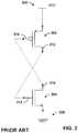
- FIG. 2 is a circuit diagram illustrating another DCAP design approach that attempts to address this issue by tying the source and body of the PFET 202 to the supply voltage 208 and the source and body of the NFET 204 to ground 206, while connecting the drain and gate nodes of the PFET and NFET in a half-cross-coupled (HCC) fashion. That is, the drain 210 of PFET 202 is connected to the gate 212 of NFET 204, while the drain 214 of NFET 204 is connected to the gate 216 of PFET 202.
- This design provides a resistive path from the supply voltage and ground nodes to the gate through device channels, thereby protecting the gate oxide during an ESD event until the ESD clamp can shunt the excess charge.
- a large channel for the design depicted in FIG. 2 will result in a high start-up time.
- This high start-up time is due to a "dead" zone in which the HCC nodes are brought up in states opposite to the values they require for the DCAP to function, and the design depends on the device leakage of the two FETS 202 and 204 to set the correct state values.
- a large channel will reduce this device leakage, resulting in a large increase in start-up time before the DCAP will be useful.
- FIG. 3 is a circuit diagram of an example DCAP circuit 300 that provides high area efficiency and high frequency operation.
- This design includes a PFET 302 and an NFET 304 connected in an HCC configuration, and area efficient capacitance (AEC) devices 306 and 308 that serve as an area efficiency decoupling capacitor.
- the AEC devices 306 and 308 can comprise, for example, a second PFET and a second NFET, respectively. With AEC devices 306 and 308 in place, the HCC devices can be optimized to provide a high frequency response without being limited by the conflicting design requirements of high area efficiency.
- the drain, source, and body of PFET AEC device 306 are connected to the supply voltage 310, while the gate 312 is connected to the PG node produced by the HCC connections.
- the drain, source, and body of NFET AEC device 308 is connected to ground 314, while the gate 316 is connected to the NG node produced by the HCC connections.
- the circuit 300 depicted in FIG. 3 allows the device channel length of the HCC devices (PFET 302 and NFET 304) - and thus the corresponding resistance of the decoupling path through the PFET and NFET - to be kept low, thereby providing high frequency supply noise decoupling. Keeping the device channel length low also increases leakage in the HCC devices, thereby keeping start-up times low for scenarios in which the HCC connectivity is initialized to the incorrect states.
- the AEC devices 306 and 308 can be optimized to provide high area efficiency.
- the AEC devices 306 and 308 can be sized to provide high area efficiency without changing the channel length (and resistance) of the decoupling path through the PFET 302 and NFET 304, and thus without changing the operating frequency of the circuit 300.
- optimizing the AEC devices 306 and 308 for high area efficiency corresponds to having a large length (L).
- circuit 300 includes two AEC devices 306 and 308 corresponding to the PFET 302 and NFET 304, respectively, some embodiments may include only one AEC device.
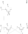
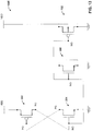
- FIG. 4 illustrates an embodiment in which only the PFET AEC device 306 is connected to the HCC circuit (omitting the NFET AEC device 308)
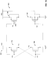
- FIG. 5 illustrates an embodiment in which only the NFET AEC device 308 is connected (omitting the PFET AEC device 306).
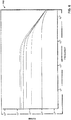
- FIG. 6 is a graph 602 illustrating the frequency response for circuit 300 for various sizes of AEC devices 306 and 308.
- Each plot of graph 602 represents the frequency response for a given size of AEC devices 306 and 308, with the sizes of the HCC devices 302 and 304 kept constant for each plot.
- the roll-off frequency ⁇ - that is, the frequency at which the capacitance of circuit 300 loses its effectiveness - is characterized by 1/(RC), where R is the resistance of the decoupling path determined by the size of the HCC devices 302 and 304, and C is the capacitance determined by the size of the AEC devices 306 and 308.
- the roll-off frequency ⁇ decreases.
- the HCC devices 302 and 304 can also be increased in order keep up with the increased capacitance of the AEC devices and thereby maintain high frequency supply noise decoupling.
- the ratio between the sizes of the HCC devices 302 and 304 to the capacitance on the AEC devices 306 and 308 determines the degree of high frequency operation.
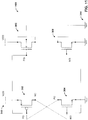
- FIG. 7 is a circuit diagram of an example DCAP circuit 700 that includes an AEC device 702 comprising a PFET having gate 704 tied to the NG node, source and drain tied to ground 314, and body tied to VDD 310.
- FIG. 8 is a circuit diagram of an example DCAP circuit 800 that includes an AEC device 802 comprising an NFET having gate 804 tied to node PG, drain and source tied to VDD 310, and body tied to ground 314.
- FIG. 9 is a circuit diagram of an example DCAP circuit 900 that includes both AEC devices 702 and 802.
- FIG. 10 is a circuit diagram of an example DCAP circuit 1000 that includes AEC device 702 and AEC device 306, while FIG. 11 is a circuit diagram of an example DCAP circuit 1100 that includes AEC device 802 and AEC device 308.
- FIG. 12 is a circuit diagram of another example DCAP circuit 1200 that includes AEC devices 306 and 802. In this example, the gates of both AEC devices are connected to the PG node.
- FIG. 13 is a circuit diagram of yet another example DECAP circuit 1300 that includes AEC devices 308 and 702. In this example, the gates of both AEC devices are connected to the NG node.
- any of circuits 300, 400, 500, 700, 800, 900, 1000, 1100, 1200, and/or 1300 can be embodied as an integrated circuit that can be used to provide supply noise suppression for a power distribution network of a VLSI system.
- Any of circuits 300, 400, 500, 700, 800, 900, 1000, 1100, 1200, or 1300 can be implemented as an on-chip component of such VLSI systems, or as an off-chip component embodied on a dedicated integrated circuit that provides supply voltage suppression for a VLSI system residing on a separate chip.
- any of circuits, 400, 500, 700, 800, 900, 1000, 1100, 1200, or 1300 may be constructed using solid state components.
- FIG. 14 illustrates a methodology in accordance with one or more embodiments. While the methodology shown herein is shown as a series of acts, the subject innovation is not limited by the order of acts, as some acts may, in accordance therewith, occur in a different order and/or concurrently with other acts from that shown and described herein. For example, those skilled in the art will understand and appreciate that a methodology could alternatively be represented as a series of interrelated states or events, such as in a state diagram. Moreover, not all illustrated acts may be required to implement a methodology in accordance with the innovation. Furthermore, interaction diagram(s) may represent methodologies, or methods, in accordance with the subject disclosure when disparate entities enact disparate portions of the methodologies. Further yet, two or more of the disclosed example methods can be implemented in combination with each other, to accomplish one or more features or advantages described herein.
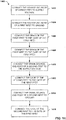
- FIG. 14 is a flow diagram of an embodiment for assembling a decoupling capacitor (DCAP) circuit.
- the DCAP circuit can be used, for example as a component of power distribution networks (PDNs).
- Method 1400 can begin at block 1402, where the source and body of a first p-channel field effect transistor (PFET) is connected to a supply voltage (e.g., a supply voltage of a power distribution network or other system requiring supply noise suppression).
- PFET p-channel field effect transistor
- NFET n-channel field effect transistor
- the drain of the first PFET is connected to the gate of the first NFET.
- the drain of the first NFET is connected to the gate of the first PFET.
- the drain, source, and body of a second PFET is connected to the supply voltage.
- the gate of the second PFET is connected to the gate of the first PFET.
- the drain, source, and body of a second NFET is connected to ground.
- the gate of the second NFET is connected to the gate of the first NFET.
- the circuit yielded by blocks 1402-1416 can be used to suppress power supply noise, and can achieve high area efficiency as well as high frequency operation.
- either of the second PFET or the second NFET can be omitted from the circuit (see, e.g., FIGS. 4 and 5 ). That is, in some embodiments, blocks 1410 and 1412 can be omitted, while in other embodiments blocks 1414 and 1416 can be omitted.
- Computer-readable media can include hardware media, software media, non-transitory media, or transport media.
Landscapes
- Semiconductor Integrated Circuits (AREA)
- Metal-Oxide And Bipolar Metal-Oxide Semiconductor Integrated Circuits (AREA)
Applications Claiming Priority (3)
| Application Number | Priority Date | Filing Date | Title |
|---|---|---|---|
| US14/736,882 US9438225B1 (en) | 2015-06-11 | 2015-06-11 | High efficiency half-cross-coupled decoupling capacitor |
| PCT/US2015/042798 WO2016200411A1 (fr) | 2015-06-11 | 2015-07-30 | Condensateur de découplage à demi-couplage croisé à efficacité élevée |
| EP15895123.6A EP3308464B1 (fr) | 2015-06-11 | 2015-07-30 | Condensateur de découplage à demi-couplage croisé à efficacité élevée |
Related Parent Applications (2)
| Application Number | Title | Priority Date | Filing Date |
|---|---|---|---|
| EP15895123.6A Division EP3308464B1 (fr) | 2015-06-11 | 2015-07-30 | Condensateur de découplage à demi-couplage croisé à efficacité élevée |
| EP15895123.6A Division-Into EP3308464B1 (fr) | 2015-06-11 | 2015-07-30 | Condensateur de découplage à demi-couplage croisé à efficacité élevée |
Publications (2)
| Publication Number | Publication Date |
|---|---|
| EP3934101A2 true EP3934101A2 (fr) | 2022-01-05 |
| EP3934101A3 EP3934101A3 (fr) | 2022-04-27 |
Family
ID=56878301
Family Applications (2)
| Application Number | Title | Priority Date | Filing Date |
|---|---|---|---|
| EP15895123.6A Active EP3308464B1 (fr) | 2015-06-11 | 2015-07-30 | Condensateur de découplage à demi-couplage croisé à efficacité élevée |
| EP21193202.5A Pending EP3934101A3 (fr) | 2015-06-11 | 2015-07-30 | Condensateur de découplage à demi-couplage croisé à efficacité élevée |
Family Applications Before (1)
| Application Number | Title | Priority Date | Filing Date |
|---|---|---|---|
| EP15895123.6A Active EP3308464B1 (fr) | 2015-06-11 | 2015-07-30 | Condensateur de découplage à demi-couplage croisé à efficacité élevée |
Country Status (5)
| Country | Link |
|---|---|
| US (1) | US9438225B1 (fr) |
| EP (2) | EP3308464B1 (fr) |
| JP (1) | JP6437674B2 (fr) |
| CN (1) | CN108141214B (fr) |
| WO (1) | WO2016200411A1 (fr) |
Families Citing this family (4)
| Publication number | Priority date | Publication date | Assignee | Title |
|---|---|---|---|---|
| US10032763B2 (en) * | 2016-06-02 | 2018-07-24 | Qualcomm Incorporated | Bulk cross-coupled high density power supply decoupling capacitor |
| US10892260B2 (en) * | 2019-03-06 | 2021-01-12 | Himax Technologies Limited | Capacitor |
| US11244895B2 (en) | 2020-06-01 | 2022-02-08 | Qualcomm Incorporated | Intertwined well connection and decoupling capacitor layout structure for integrated circuits |
| KR102861814B1 (ko) | 2020-09-29 | 2025-09-17 | 삼성전자주식회사 | 비대칭 디커플링 셀을 포함하는 집적 회로 및 이를 설계하는 방법 |
Family Cites Families (25)
| Publication number | Priority date | Publication date | Assignee | Title |
|---|---|---|---|---|
| US5266848A (en) * | 1990-03-28 | 1993-11-30 | Hitachi, Ltd. | CMOS circuit with reduced signal swing |
| SE470415B (sv) | 1992-07-06 | 1994-02-14 | Ericsson Telefon Ab L M | Kondensator med hög kapacitans i ett integrerat funktionsblock eller en integrerad krets, förfarande för framställning av kondensatorn och användning av kondensatorn som en integrerad avkopplingskondensator |
| JPH08102652A (ja) | 1994-10-03 | 1996-04-16 | Seiko Epson Corp | 半導体集積回路 |
| JPH08307229A (ja) | 1995-04-28 | 1996-11-22 | Fuji Electric Co Ltd | 負荷駆動回路 |
| JPH0993111A (ja) | 1995-09-28 | 1997-04-04 | Toshiba Microelectron Corp | スルーレート型バッファ回路 |
| JPH09148909A (ja) | 1995-11-17 | 1997-06-06 | Hitachi Ltd | 半導体集積回路装置 |
| US5883423A (en) * | 1996-02-23 | 1999-03-16 | National Semiconductor Corporation | Decoupling capacitor for integrated circuit signal driver |
| JPH11186497A (ja) * | 1997-12-17 | 1999-07-09 | Toshiba Corp | 半導体集積回路装置 |
| JP3838769B2 (ja) | 1997-12-25 | 2006-10-25 | 川崎マイクロエレクトロニクス株式会社 | 出力バッファ回路 |
| JP2000286388A (ja) * | 1999-03-30 | 2000-10-13 | Advantest Corp | 半導体デバイス |
| US6936917B2 (en) | 2001-09-26 | 2005-08-30 | Molex Incorporated | Power delivery connector for integrated circuits utilizing integrated capacitors |
| JP4342833B2 (ja) * | 2003-05-16 | 2009-10-14 | Necエレクトロニクス株式会社 | 容量セルと半導体装置及びその製造方法 |
| KR100592787B1 (ko) | 2004-11-09 | 2006-06-26 | 삼성전자주식회사 | 링 형태의 실리콘 디커플링 커패시터를 가지는 집적회로칩 패키지 |
| JP2006203801A (ja) * | 2005-01-24 | 2006-08-03 | Fujitsu Ltd | バッファ回路及び集積回路 |
| US8160824B2 (en) | 2005-01-27 | 2012-04-17 | Electro Industries/Gauge Tech | Intelligent electronic device with enhanced power quality monitoring and communication capabilities |
| JP4841204B2 (ja) * | 2005-08-31 | 2011-12-21 | ルネサスエレクトロニクス株式会社 | 半導体装置 |
| JP5092263B2 (ja) * | 2006-03-31 | 2012-12-05 | 富士通セミコンダクター株式会社 | デカップリングコンデンサ及び半導体集積回路装置 |
| US7903679B1 (en) | 2006-04-11 | 2011-03-08 | Altera Corporation | Power supply filtering for programmable logic device having heterogeneous serial interface architecture |
| US8134824B2 (en) * | 2008-02-19 | 2012-03-13 | Arm Limited | Decoupling capacitors |
| JP2009246062A (ja) * | 2008-03-31 | 2009-10-22 | Hitachi Ltd | 半導体集積回路装置、および、その製造方法 |
| US8345396B2 (en) * | 2010-03-08 | 2013-01-01 | Macronix International Co., Ltd. | Electrostatic discharge protectors having increased RC delays |
| US8539422B2 (en) | 2011-02-24 | 2013-09-17 | Cadence Design Systems, Inc. | Method and system for power delivery network analysis |
| US9029173B2 (en) | 2011-10-18 | 2015-05-12 | Monolithic 3D Inc. | Method for fabrication of a semiconductor device and structure |
| JP5812103B2 (ja) * | 2011-11-14 | 2015-11-11 | 日本電気株式会社 | デカップリング回路及び半導体集積回路 |
| US8963575B2 (en) * | 2012-09-26 | 2015-02-24 | Sandisk Technologies Inc. | Analog majority vote circuit |
-
2015
- 2015-06-11 US US14/736,882 patent/US9438225B1/en active Active
- 2015-07-30 WO PCT/US2015/042798 patent/WO2016200411A1/fr not_active Ceased
- 2015-07-30 EP EP15895123.6A patent/EP3308464B1/fr active Active
- 2015-07-30 CN CN201580080820.9A patent/CN108141214B/zh active Active
- 2015-07-30 EP EP21193202.5A patent/EP3934101A3/fr active Pending
- 2015-07-30 JP JP2017564018A patent/JP6437674B2/ja active Active
Also Published As
| Publication number | Publication date |
|---|---|
| JP2018521504A (ja) | 2018-08-02 |
| EP3934101A3 (fr) | 2022-04-27 |
| US9438225B1 (en) | 2016-09-06 |
| WO2016200411A1 (fr) | 2016-12-15 |
| EP3308464B1 (fr) | 2021-10-06 |
| EP3308464A4 (fr) | 2019-05-08 |
| CN108141214B (zh) | 2019-06-11 |
| CN108141214A (zh) | 2018-06-08 |
| JP6437674B2 (ja) | 2018-12-12 |
| EP3308464A1 (fr) | 2018-04-18 |
Similar Documents
| Publication | Publication Date | Title |
|---|---|---|
| CN104319275B (zh) | 静电放电保护电路 | |
| US20130182356A1 (en) | ESD Clamp with Novel RC Triggered Circuit | |
| US20130155556A1 (en) | Electrostatic discharge protection circuit and method for radio frequency semiconductor device | |
| US9373612B1 (en) | Electrostatic discharge protection circuits and methods | |
| US20180024187A1 (en) | Semiconductor integrated circuit | |
| US8817437B2 (en) | High voltage open-drain electrostatic discharge (ESD) protection device | |
| JP2014132717A (ja) | 静電気放電保護回路及び半導体回路装置 | |
| EP3308464B1 (fr) | Condensateur de découplage à demi-couplage croisé à efficacité élevée | |
| US9379707B2 (en) | Decoupling circuit and semiconductor integrated circuit | |
| US10404265B1 (en) | Current-mode feedback source follower with enhanced linearity | |
| US8345396B2 (en) | Electrostatic discharge protectors having increased RC delays | |
| US20190214983A1 (en) | Clock voltage step-up circuit | |
| CN103247697A (zh) | 去耦电容器及具有该去耦电容器的集成电路 | |
| US9859704B2 (en) | Node isolation for protection from electrostatic discharge (ESD) damage | |
| US20160126937A1 (en) | Latch and frequency divider | |
| EP3447800B1 (fr) | Circuit de filtre à base de transistor à effet de champ mos et puce | |
| CN102655406B (zh) | 接收电路 | |
| KR102101537B1 (ko) | 타이하이 및 타이로우 회로 | |
| CN110263468B (zh) | 一种片内cmos电容及一种芯片 | |
| US10320351B1 (en) | Switch for controlling a gain of an amplifier and method thereof | |
| TW202227834A (zh) | 去耦合電容的漏電流阻擋電路和漏電流阻擋方法 | |
| TWI234264B (en) | ESD protection circuit with a stack-coupling device | |
| JP2014204602A (ja) | 半導体装置 | |
| US9093966B1 (en) | ESD protection circuit for cascode amplifiers | |
| US9264032B2 (en) | Voltage protection scheme for semiconductor devices |
Legal Events
| Date | Code | Title | Description |
|---|---|---|---|
| PUAI | Public reference made under article 153(3) epc to a published international application that has entered the european phase |
Free format text: ORIGINAL CODE: 0009012 |
|
| STAA | Information on the status of an ep patent application or granted ep patent |
Free format text: STATUS: THE APPLICATION HAS BEEN PUBLISHED |
|
| AC | Divisional application: reference to earlier application |
Ref document number: 3308464 Country of ref document: EP Kind code of ref document: P |
|
| AK | Designated contracting states |
Kind code of ref document: A2 Designated state(s): AL AT BE BG CH CY CZ DE DK EE ES FI FR GB GR HR HU IE IS IT LI LT LU LV MC MK MT NL NO PL PT RO RS SE SI SK SM TR |
|
| PUAL | Search report despatched |
Free format text: ORIGINAL CODE: 0009013 |
|
| AK | Designated contracting states |
Kind code of ref document: A3 Designated state(s): AL AT BE BG CH CY CZ DE DK EE ES FI FR GB GR HR HU IE IS IT LI LT LU LV MC MK MT NL NO PL PT RO RS SE SI SK SM TR |
|
| RIC1 | Information provided on ipc code assigned before grant |
Ipc: H01L 29/94 20060101ALN20220322BHEP Ipc: H01L 27/08 20060101ALN20220322BHEP Ipc: H01L 27/06 20060101ALI20220322BHEP Ipc: H01L 27/02 20060101AFI20220322BHEP |
|
| STAA | Information on the status of an ep patent application or granted ep patent |
Free format text: STATUS: REQUEST FOR EXAMINATION WAS MADE |
|
| 17P | Request for examination filed |
Effective date: 20221021 |
|
| RBV | Designated contracting states (corrected) |
Designated state(s): AL AT BE BG CH CY CZ DE DK EE ES FI FR GB GR HR HU IE IS IT LI LT LU LV MC MK MT NL NO PL PT RO RS SE SI SK SM TR |