EP3937227B1 - Halbleiterbauelementpaket mit einem thermischen schnittstellenmaterial mit verbesserten handhabungseigenschaften - Google Patents
Halbleiterbauelementpaket mit einem thermischen schnittstellenmaterial mit verbesserten handhabungseigenschaften Download PDFInfo
- Publication number
- EP3937227B1 EP3937227B1 EP20185063.3A EP20185063A EP3937227B1 EP 3937227 B1 EP3937227 B1 EP 3937227B1 EP 20185063 A EP20185063 A EP 20185063A EP 3937227 B1 EP3937227 B1 EP 3937227B1
- Authority
- EP
- European Patent Office
- Prior art keywords
- package
- die
- semiconductor device
- device package
- carrier
- Prior art date
- Legal status (The legal status is an assumption and is not a legal conclusion. Google has not performed a legal analysis and makes no representation as to the accuracy of the status listed.)
- Active
Links
Images


Classifications
-
- H—ELECTRICITY
- H10—SEMICONDUCTOR DEVICES; ELECTRIC SOLID-STATE DEVICES NOT OTHERWISE PROVIDED FOR
- H10W—GENERIC PACKAGES, INTERCONNECTIONS, CONNECTORS OR OTHER CONSTRUCTIONAL DETAILS OF DEVICES COVERED BY CLASS H10
- H10W40/00—Arrangements for thermal protection or thermal control
- H10W40/20—Arrangements for cooling
- H10W40/25—Arrangements for cooling characterised by their materials
- H10W40/251—Organics
-
- H—ELECTRICITY
- H10—SEMICONDUCTOR DEVICES; ELECTRIC SOLID-STATE DEVICES NOT OTHERWISE PROVIDED FOR
- H10W—GENERIC PACKAGES, INTERCONNECTIONS, CONNECTORS OR OTHER CONSTRUCTIONAL DETAILS OF DEVICES COVERED BY CLASS H10
- H10W40/00—Arrangements for thermal protection or thermal control
- H10W40/70—Fillings or auxiliary members in containers or in encapsulations for thermal protection or control
-
- H—ELECTRICITY
- H10—SEMICONDUCTOR DEVICES; ELECTRIC SOLID-STATE DEVICES NOT OTHERWISE PROVIDED FOR
- H10W—GENERIC PACKAGES, INTERCONNECTIONS, CONNECTORS OR OTHER CONSTRUCTIONAL DETAILS OF DEVICES COVERED BY CLASS H10
- H10W40/00—Arrangements for thermal protection or thermal control
- H10W40/20—Arrangements for cooling
- H10W40/25—Arrangements for cooling characterised by their materials
- H10W40/255—Arrangements for cooling characterised by their materials having a laminate or multilayered structure, e.g. direct bond copper [DBC] ceramic substrates
-
- H—ELECTRICITY
- H10—SEMICONDUCTOR DEVICES; ELECTRIC SOLID-STATE DEVICES NOT OTHERWISE PROVIDED FOR
- H10W—GENERIC PACKAGES, INTERCONNECTIONS, CONNECTORS OR OTHER CONSTRUCTIONAL DETAILS OF DEVICES COVERED BY CLASS H10
- H10W40/00—Arrangements for thermal protection or thermal control
- H10W40/20—Arrangements for cooling
- H10W40/25—Arrangements for cooling characterised by their materials
- H10W40/258—Metallic materials
-
- H—ELECTRICITY
- H10—SEMICONDUCTOR DEVICES; ELECTRIC SOLID-STATE DEVICES NOT OTHERWISE PROVIDED FOR
- H10W—GENERIC PACKAGES, INTERCONNECTIONS, CONNECTORS OR OTHER CONSTRUCTIONAL DETAILS OF DEVICES COVERED BY CLASS H10
- H10W74/00—Encapsulations, e.g. protective coatings
- H10W74/01—Manufacture or treatment
-
- H—ELECTRICITY
- H10—SEMICONDUCTOR DEVICES; ELECTRIC SOLID-STATE DEVICES NOT OTHERWISE PROVIDED FOR
- H10W—GENERIC PACKAGES, INTERCONNECTIONS, CONNECTORS OR OTHER CONSTRUCTIONAL DETAILS OF DEVICES COVERED BY CLASS H10
- H10W74/00—Encapsulations, e.g. protective coatings
- H10W74/10—Encapsulations, e.g. protective coatings characterised by their shape or disposition
- H10W74/111—Encapsulations, e.g. protective coatings characterised by their shape or disposition the semiconductor body being completely enclosed
- H10W74/114—Encapsulations, e.g. protective coatings characterised by their shape or disposition the semiconductor body being completely enclosed by a substrate and the encapsulations
-
- H—ELECTRICITY
- H10—SEMICONDUCTOR DEVICES; ELECTRIC SOLID-STATE DEVICES NOT OTHERWISE PROVIDED FOR
- H10W—GENERIC PACKAGES, INTERCONNECTIONS, CONNECTORS OR OTHER CONSTRUCTIONAL DETAILS OF DEVICES COVERED BY CLASS H10
- H10W74/00—Encapsulations, e.g. protective coatings
- H10W74/40—Encapsulations, e.g. protective coatings characterised by their materials
- H10W74/47—Encapsulations, e.g. protective coatings characterised by their materials comprising organic materials, e.g. plastics or resins
- H10W74/473—Encapsulations, e.g. protective coatings characterised by their materials comprising organic materials, e.g. plastics or resins containing a filler
-
- H—ELECTRICITY
- H10—SEMICONDUCTOR DEVICES; ELECTRIC SOLID-STATE DEVICES NOT OTHERWISE PROVIDED FOR
- H10W—GENERIC PACKAGES, INTERCONNECTIONS, CONNECTORS OR OTHER CONSTRUCTIONAL DETAILS OF DEVICES COVERED BY CLASS H10
- H10W40/00—Arrangements for thermal protection or thermal control
- H10W40/70—Fillings or auxiliary members in containers or in encapsulations for thermal protection or control
- H10W40/77—Auxiliary members characterised by their shape
- H10W40/778—Auxiliary members characterised by their shape in encapsulations
-
- H—ELECTRICITY
- H10—SEMICONDUCTOR DEVICES; ELECTRIC SOLID-STATE DEVICES NOT OTHERWISE PROVIDED FOR
- H10W—GENERIC PACKAGES, INTERCONNECTIONS, CONNECTORS OR OTHER CONSTRUCTIONAL DETAILS OF DEVICES COVERED BY CLASS H10
- H10W70/00—Package substrates; Interposers; Redistribution layers [RDL]
- H10W70/40—Leadframes
- H10W70/481—Leadframes for devices being provided for in groups H10D8/00 - H10D48/00
-
- H—ELECTRICITY
- H10—SEMICONDUCTOR DEVICES; ELECTRIC SOLID-STATE DEVICES NOT OTHERWISE PROVIDED FOR
- H10W—GENERIC PACKAGES, INTERCONNECTIONS, CONNECTORS OR OTHER CONSTRUCTIONAL DETAILS OF DEVICES COVERED BY CLASS H10
- H10W72/00—Interconnections or connectors in packages
- H10W72/50—Bond wires
- H10W72/531—Shapes of wire connectors
- H10W72/5363—Shapes of wire connectors the connected ends being wedge-shaped
-
- H—ELECTRICITY
- H10—SEMICONDUCTOR DEVICES; ELECTRIC SOLID-STATE DEVICES NOT OTHERWISE PROVIDED FOR
- H10W—GENERIC PACKAGES, INTERCONNECTIONS, CONNECTORS OR OTHER CONSTRUCTIONAL DETAILS OF DEVICES COVERED BY CLASS H10
- H10W74/00—Encapsulations, e.g. protective coatings
Definitions
- the present disclosure relates to a semiconductor device package.
- a general problem is to reliably dissipate the heat generated in the semiconductor die to the outside.
- a semiconductor die mounted on an electrical carrier is cast with an encapsulating compound and thereby a surface region of the electrical carrier is kept free.
- a thermal interface structure (TIM, thermal interface material), which electrically isolates the electrical carrier with respect to its surroundings, can then be mounted on one part of the encapsulation structure and the surface region of the electrical carrier.
- the user can then mount a heat dissipation element, for example in the form of a heat sink, on such a semiconductor device package, in order to be able to dissipate accumulated waste heat from the semiconductor device package to the periphery during the operation of the semiconductor device package.
- This can be advantageous in a number of different applications, e.g., EV charging, electro-mobility, renewable energy, home appliances, etc.
- thermal interface materials are used as interface material between the electrical carrier and the cooling unit.
- thermal grease different materials have been used in the past, among them, for example, thermal grease.
- thermal grease different materials have been used in the past, among them, for example, thermal grease.
- thermal grease may lack sufficient electrical isolation and are often not reliable in the way that during operation cycles their thermomechanical stability can be affected.
- dispensing of thermal grease is not properly performed leading to a possible thermal issue with the component. For example, an uneven dispensation of the thermal paste on a production line may be problematic.
- the document WO 2015/056523 A1 describes an epoxy-resin composition which is used to form an insulating resin layer that is part of a metal-based circuit board wherein the insulating resin layer is provided on top of a metal substrate and a metal layer is provided on top of the insulating resin layer.
- An aspect of the present disclosure is related to a semiconductor device package according to the features of the appended claim 1.
- the terms “bonded”, “attached”, “connected”, “coupled” and/or “electrically connected/electrically coupled” are not meant to mean that the elements or layers must directly be contacted together; intervening elements or layers may be provided between the “bonded”, “attached”, “connected”, “coupled” and/or “electrically connected/electrically coupled” elements, respectively.
- the above-mentioned terms may, optionally, also have the specific meaning that the elements or layers are directly contacted together, i.e. that no intervening elements or layers are provided between the "bonded”, “attached”, “connected”, “coupled” and/or “electrically connected/electrically coupled” elements, respectively.
- the word “over” used with regard to a part, element or material layer formed or located “over” a surface may be used herein to mean that the part, element or material layer be located (e.g. placed, formed, deposited, etc.) "indirectly on” the implied surface with one or more additional parts, elements or layers being arranged between the implied surface and the part, element or material layer.
- the word “over” used with regard to a part, element or material layer formed or located “over” a surface may, optionally, also have the specific meaning that the part, element or material layer be located (e.g. placed, formed, deposited, etc.) "directly on", e.g. in direct contact with, the implied surface.
- a semiconductor device package is provided as defined by the independent claim.
- a semiconductor device package which comprises an electrically conductive carrier, a semiconductor die disposed on the carrier, an encapsulant encapsulating part of the carrier and the semiconductor die, and an electrically insulating and thermally conductive interface structure covering an exposed surface portion of the carrier and a connected surface portion of the encapsulant, and for example to be attached at an external surface to a heat dissipation body, wherein the interface structure is made of a material having an epoxy resin matrix filled with filler particles, e.g.
- metal oxide or metal nitride filler particles for instance comprising or consisting of AlO, ZrO 2 , Si 3 N 4 , BN, AlN, diamond, etc., in particular metal oxide or metal nitride filler particles, with a mass percentage in a range between 75% and 98%, in particular in a range between 83% and 96%, more particularly in a range between 90% and 95%.
- a method of fabricating a semiconductor device package comprises mounting a semiconductor die on an electrically conductive carrier, encapsulating part of the carrier and the semiconductor die by an encapsulant, and forming, e.g. for instance encapsulating, an electrically insulating and thermally conductive interface structure, e.g. for example to cover an exposed surface portion of the carrier and a connected surface portion of the encapsulant, and for example to be attached at an external surface to a heat dissipation body, wherein the interface structure is made of a material having an epoxy resin matrix filled with filler particles, e.g.
- metal oxide and/or metal nitride filler particles comprising or consisting of AlO, ZrO 2 , Si 3 N 4 , BN, AlN, diamond, etc., in particular metal oxide and/or metal nitride filler particles, with a mass percentage in a range between 75% and 98%, in particular in a range between 90% and 95%.
- an semiconductor device package which comprises an electrically conductive carrier which comprises a plurality of galvanically insulated separate carrier regions, in particular a plurality of carrier regions being provided separately from one another and being mutually spaced so as to form mutually galvanically insulated islands, a plurality of semiconductor dies each of which being mounted on a respective one of the carrier regions, an encapsulant encapsulating part of the carrier and the semiconductor dies, and a common electrically insulating and thermally conductive interface structure, in particular a continuous or an integral structure spatially extending beyond the multiple carrier regions and assigned semiconductor dies, covering an exposed surface portion of the carrier regions and a connected surface portion of the encapsulant.
- a method of fabricating a semiconductor device package comprises mounting each of a plurality of semiconductor dies on a respective one of a plurality of galvanically insulated separate carrier regions of an electrically conductive carrier, encapsulating part of the carrier and the electronic dies by an encapsulant, and forming a common electrically insulating and thermally conductive interface structure covering an exposed surface portion of the carrier regions and a connected surface portion of the encapsulant.
- an interface material having the above-mentioned features is used for providing an electric isolation and a thermal coupling between a die carrier of a semiconductor device package and a heat dissipation body or cooling unit.
- a thermal interface material with a specified range of the glass transition temperature Tg is provided.
- a thermal interface material with this property can comprise a sufficient hardness and scratch resistance at room temperature in terms of handling and mounting and also a sufficient softness and compressibility at operating temperatures above 60°C. More specifically, a thermal interface material can be selected which has a Tg value between room temperature and the operating temperature such that handling and mounting of the semiconductor device package on the customer's side may be done with a TIM layer of very high hardness and scratch resistance and operating the semiconductor device package may be done with a TIM layer of high softness and compressibility and low modulus.
- a sufficiently soft and sufficiently stable interface structure can be obtained which has the mechanical softness of filling gaps to improve thermal coupling and provides the mechanical rigidity for reliably ensuring electric insulation even in the presence of scratch or delamination forces.
- the thermal interface material is capable of filling substantially any microgaps at a surface of a heat dissipation body, thereby improving the external thermal coupling.
- the thermal interface material on the package is therefore pressed against the heat dissipation body, no or at least no major thermal gaps in form of microscopic air volumes occur.
- a too soft property is avoided which might have an undesired impact on the electrical reliability and a delamination danger of the thermal interface material.
- a robust (in terms of handling and mounting) and scratch resistant solution is provided. With appropriate compressibility values, it can be achieved that the material of the thermal interface structure properly adapts itself to the material of the heat sink.
- thermal interface material from an epoxy resin matrix in which a sufficiently large amount of properly thermally conductive and electrically insulating filler particles (for instance of metal oxide and/or metal nitride, in particular of at least one of the group consisting of Zr0 2 , Si 3 N 4 , BN, AlN, diamond, etc.) are embedded.
- a single common thermal interface structure (for instance a common thermal interface layer) may cover a plurality of mutually galvanically insulated carrier regions, wherein each of the carrier regions carries a respective one of multiple electronic dies.
- thermal interface structure for the multiple die carrier regions may be performed in one single common procedure, and thus very efficiently.
- thermal interface structure with the described advantageous characteristics onto a carrier (and optionally additionally onto an encapsulant) of an electronic component, which is to be attached, in turn, to a heat dissipation body
- Such a heat dissipation body with the attached thermal interface structure thereon may then be attached onto an exposed surface portion of a carrier of an electronic component which itself does not have a thermal interface structure on the exposed surface of its carrier.
- the interface structure has at a temperature of 100°C a hardness in a range between 10 MPa and 100 MPa, more specifically the lower bound of the range being 20 MPa, 30 MPa, 40 MPa, or 50 MPa, more specifically the upper bound of the range being 90 MPa, 80 MPa, 70 MPa, or 60 MPa.
- the term "hardness”, also named “Vickers hardness”, may particularly denote a standardized microhardness of the material of the thermal interface structure.
- an indenter in form of a pyramid-shaped diamond body may be pressed with a defined force against a surface of the thermal interface material and the resulting protrusion or displacement depth is measured.
- the indenter may be embodied as a diamond in the form of a square-based pyramid which results in an indenter shape being capable of producing geometrically similar impressions irrespective of size, in an impression which has well-defined points of measurement, and in an indenter which has high resistance to self-deformation.
- the Vickers hardness (HV number) can then be determined by the ratio F/A, wherein F is the force applied to the diamond and A is the surface area of the resulting indentation.
- the interface structure comprises a thickness in a range between 50 ⁇ m and 1000 ⁇ m, more specifically the lower bound of the range being 60 ⁇ m, 70 ⁇ m, 80 ⁇ m, 90 ⁇ m, or 100 ⁇ m, more specifically the upper bound of the range being 900 ⁇ m, 800 ⁇ m, 700 ⁇ m, 600 ⁇ m, 500 ⁇ m, 400 ⁇ m, 300 ⁇ m, or 200 ⁇ m.
- the thickness may be around 250 ⁇ m.
- Sufficiently high thicknesses of the thermal interface material allow for a reliable dielectric or electrically insulating separation between the carrier in an interior of the package and an exterior thereof. However, the thicker the thermal interface material, the stronger will the thermal energy removal capability of the thermal interface structure be influenced.
- the given range allows to obtain both proper thermal conditions and electrical conditions at the same time. Also a scratch resistance may be ensured with the mentioned thicknesses even under harsh conditions.
- the interface structure has a thermal conductivity of at least 1 Wm -1 K -1 , in particular of at least 2 Wm -1 K -1 , more particularly in a range between 3 Wm -1 K -1 and 25 Wm -1 K -1 .
- the thermal interface material shall be properly electrically insulating and thermally conductive at the same time. To obtain this, the physical boundary conditions are challenging. However, it has turned out that the mentioned values of thermal conductivity are on the one hand higher than those of typical encapsulants (such as a mold compound) so that the thermal interface material efficiently removes heat from the package, and also allow to provide the thermal interface material with sufficient dielectric properties.
- the interface structure consists of a single layer. Therefore, it is dispensable to provide complex layer stacks of multiple layers for meeting the various thermomechanical and electrical properties at the same time.
- a single layer has turned out to be sufficient. This also reduces the effort for forming the thermal interface structure.
- the thermal interface structure may comprise a polymer, in particular a polymer matrix.
- the polymer matrix may e.g. comprise or consist of an epoxy material. It is also possible to configure the matrix from a polymer mixture of silicone and epoxy material. Furthermore, it is possible to use polyimide and/or polyacrylate and/or cyanate ester and/or BMI (Bis-Maleimides) and/or Novolac and/or amine as matrix material.
- a thermoplastic material may be used as matrix material. Such a thermoplast may provide a high softness in particular at high temperatures allowing the interface material to adjust itself to a contact surface in particular at high temperature values.
- the various materials mentioned as examples for the matrix may also be combined to form a multi material matrix.
- the filler particles comprise or consist of at least one of the group consisting of aluminum oxide, silicon oxide, boron nitride, zirconium oxide, silicon nitride, diamond and aluminum nitride. Any kind of mixture or combination between these and other filler particles is possible. With the mentioned materials for the filler particles, for instance microscopic spheres or beads, in particular thermal conductivity and dielectric behaviour may be promoted.
- one or more physical properties of the interface material may be tuned (such as moisture protection, adhesion promotion, improvement of the thermal conductivity, etc.).
- a mass percentage of the filler particles is at least 80%, in particular at least 90%.
- matrix material for instance silicone or epoxy-based materials
- the thermal interface structure is made of a material which is a ceramic compound, for instance aluminium oxide particles in a silicone grid.
- the semiconductor device package is configured as one out of the group consisting of a leadframe connected power module, a Transistor Outline (TO) electronic component, a Quad Flat No Leads Package (QFN) package, a Small Outline (SO) package, a Small Outline Transistor (SOT) package, and a Thin Small Outline Package (TSOP) package. Therefore, the package according to an exemplary embodiment is fully compatible with standard packaging concepts (in particular fully compatible with standard TO packaging concepts) and appears externally as a conventional package, which is highly user-convenient.
- the package is configured as a power module, for instance molded power module.
- an exemplary embodiment of the package may be an intelligent power module (IPM).
- Another exemplary embodiment of the package is a dual inline package (DIP).
- the interface structure extends over an entire main surface of the encapsulant and over the entire exposed surface portion of the carrier at a main surface of the electronic component.
- one entire main surface of the package may be coated with the thermal interface material. This can be a result of the manufacturing procedure of the thermal interface material which is preferably not based on the attachment of a thermal interface foil to the package, but in contrast to this, an integral formation of the thermal interface material by molding or lamination is performed. Furthermore, such a full coating of one entire surface of the package with a thermal interface structure further improves the mechanical robustness and the suppression of the danger of undesired creeping currents between an interior and an exterior of the package.
- the size of the thermal interface structure fits exactly to a size of the package.
- the outline of the thermal interface structure and of one main surface of the package are identical.
- the thermal interface layer may be also smaller than the package area in a fan-in structure.
- the carrier comprises a plurality of sections of different thickness. This increases the design flexibility in terms of electrical and mechanical properties of different sections of the carrier. Alternatively, it is possible that the carrier has a homogeneous thickness over its entire extension.
- the interface structure is formed (in particular encapsulated) by at least one of the group consisting of molding, in particular compression molding or transfer molding, stencil printing, and laminating.
- molding in particular compression molding or transfer molding, stencil printing, and laminating.
- such manufacturing methods may promote the formation of an integral thermal interface which may also intermingle with carrier and/or encapsulant
- a generative or an additive (for instance software controlled) manufacturing procedure such as printing, in particular three-dimensional printing. The mentioned manufacturing procedures are therefore preferred over the attachment of a thermal interface foil on the remainder of the package.
- the thermal interface structure may be connected to the remainder of the package by the application of pressure and heat, optionally under vacuum, preferably accompanied by a curing reaction.
- the interface structure is connected to the exposed surface portion of the carrier and to the connected surface portion of the encapsulant by chemically modifying the material of the interface structure, in particular by at least one of the group consisting of cross-linking and melting or any chemical reaction.
- the integral character of thermal interface material with carrier and/or encapsulant may be further promoted by a chemical reaction initiating the formation of the thermal interface structure.
- the thermal interface structure according to an exemplary embodiment of the disclosure is easy to use and provides a plug-and-play package, since no further material (such as unreliable thermal grease and/or paste) is required between the package and the heat sink. Since the handling of thermal grease is dispensable according to exemplary embodiments of the disclosure, there remains no danger that a customer unintentionally influences performance of the electronic device by an unskilled handling of the thermally grease.
- Thermal conductivity of the material of the interface structure may be higher than thermal conductivity of the material of the encapsulant.
- thermal conductivity of the material of the encapsulant may be in a range between 0.8 Wm -1 K -1 and 8 Wm -1 K -1 , in particular in a range between 2 Wm -1 K -1 and 4 Wm -1 K -1 .
- the material of the interface structure may be an epoxy resin based material (or may be made on the basis of any other resin-based material, and/or combinations thereof) which may comprise filler particles for improving thermal conductivity.
- such filler particles may comprise or consist of aluminum oxide (and/or boron nitride, aluminum nitride, diamond, silicon nitride).
- values of 15 Wm -1 K -1 may be obtained, possibly values in a range between 20 Wm -1 K -1 and 30 Wm -1 K -1 .
- the carrier comprises or consists of a leadframe.
- a leadframe may be a metal structure inside a die package that is configured for carrying signals from the electronic die to the outside, and/or vice versa.
- the electronic die inside the package or electronic component may be attached to the leadframe, and then bond wires may be provided for attach pads of the electronic die to leads of the leadframe.
- the leadframe may be moulded in a plastic case or any other encapsulant. Outside of the leadframe, a corresponding portion of the leadframe may be cut-off, thereby separating the respective leads. Before such a cut-off, other procedures such a plating, final testing, packing, etc. may be carried out, as known by those skilled in the art.
- Leadframe or die carrier can be coated before encapsulation, for instance by an adhesion promoter.
- the semiconductor device package further comprises the above-mentioned heat dissipation body attached or to be attached to the interface structure for dissipating heat generated by the electronic die during operation of the package.
- the heat dissipation body may be a plate of a properly thermally conductive body, such as copper or aluminium or graphite, diamond, composite material and/or combinations of the mentioned and/or other materials, which may have cooling fins or the like to further promote dissipation of heat which can be thermally conducted from the electronic die via the die carrier and the interface structure to the heat dissipation body.
- the removal of the heat via the heat dissipation body may further be promoted by a cooling fluid such as air or water (more generally a gas and/or a liquid) which may flow along the heat dissipation body externally of the electronic component.
- a cooling fluid such as air or water (more generally a gas and/or a liquid) which may flow along the heat dissipation body externally of the electronic component.
- heat pipes may be implemented.
- the semiconductor device package is adapted for double-sided cooling.
- a first interface structure may thermally couple the encapsulated die and carrier with a first heat dissipation body
- a second interface structure may thermally couple the encapsulated die and carrier with a second heat dissipation body.
- the semiconductor die is configured as a power semiconductor die.
- the semiconductor die (such as a semiconductor die) may be used for power applications for instance in the automotive field and may for instance have at least one integrated insulated-gate bipolar transistor (IGBT) and/or at least one transistor of another type (such as a MOSFET, a JFET, etc.) and/or at least one integrated diode.
- IGBT integrated insulated-gate bipolar transistor
- Such integrated circuit elements may be made for instance in silicon technology or based on wide-bandgap semiconductors (such as silicon carbide).
- a semiconductor power die may comprise one or more field effect transistors, diodes, inverter circuits, half-bridges, full-bridges, drivers, logic circuits, further devices, etc.
- the semiconductor die experiences a vertical current flow.
- the package architecture according to exemplary embodiments of the disclosure is particularly appropriate for high power applications in which a vertical current flow is desired, i.e. a current flow in a direction perpendicular to the two opposing main surfaces of the electronic die, one of which being used for mounting the semiconductor die on the carrier.
- a semiconductor substrate preferably a silicon substrate
- a silicon oxide or another insulator substrate may be provided.
- a germanium substrate or a III-V-semiconductor material For instance, exemplary embodiments may be implemented in GaN or SIC technology.
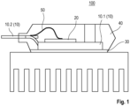
- Fig. 1 shows a schematic cross-sectional side view representation of a semiconductor device package of the first aspect according to an example.
- the semiconductor device package 100 of Fig. 1 comprises electrically conductive carrier 10, a semiconductor die 20 disposed on the carrier 10, an encapsulant 40 encapsulating part of the carrier 10 and the semiconductor die 20, an electrically insulating and thermally conductive interface structure 30, covering an exposed surface portion of the carrier 10 and a connected surface portion of the encapsulant 40, wherein the interface structure 30 is made of an epoxy resin material and comprises a glass transition temperature of about 35°C.
- the resin matrix of the interface structure 30 is filled with filler particles made of aluminum oxide, wherein the mass percentage of the filler particles in the epoxy resin material is about 95%.
- the carrier 10 is a leadframe 10 which comprises a die pad 10.1 for mounting the semiconductor die 20 thereon and a plurality of external leads 10.2 at least one of which is connected with an upper contact pad of the semiconductor die 20 by a bond wire 50.
- the semiconductor die 20 is an IGBT die and the semiconductor device package 100 is a TO package.
- the semiconductor device package 100 can be mounted on a heatsink 60.
- the heatsink 60 is made of an aluminum block comprising a plurality of fins 61 for improving the heat dissipation to the environment.
- Fig. 2 shows a diagram plotting the measured displacement into the sample surface in dependence on the load on the sample for epoxy materials according to the disclosure and known silicone materials.
- the measurements were done as was described before, namely by pressing an indenter in the form of a pyramid-shaped diamond body with a defined force against a surface of the thermal interface material and by measuring the resulting displacement depth. The measurements were done at a temperature T of 22°.
- the differently grey shaded areas I and II show the measurement results for a material according to the present disclosure (I) and for previously used silicone-based materials (II).
- the lower curve of I shows measurements performed with the thermal interface material as was shown and described in connection with Fig. 1 hence at Tg > T.
- the curves of II show measurement results of two different silicone materials.
- Fig. 3 shows a bar diagram depicting the measured heat resistance Rth between an epoxy material according to the disclosure and an aluminum heat sink in dependence on the temperature
- Fig. 4 comprising Fig. 4A and 4B schematically illustrates the situation at the contact zone between the thermal interface material and the heatsink at different temperatures.
- the values of Rth continuously decrease from a relatively high value of 1.7 K/W at a temperature of 25°C down to a value of below 1.5 K/W at a temperature of 150°C.
- This decrease can be explained by a softening of the thermal interface layer and corresponding flowing and creeping of the thermal interface material into hollow spaces and indentations in the surface of the heatsink which leads to an increase of the contact area and a corresponding increase of heat flow.
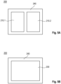
- Fig. 5 comprises Fig. 5A and 5B and shows a down view of an exemplary semiconductor device package comprising two electrically separated carrier regions (5A) which can be covered with a common TIM structure (5B).
- the semiconductor device package 200 as shown in Fig. 5 is an example for the above described embodiment in which a semiconductor device package is provided with a plurality of galvanically insulated separate carrier regions, in particular a plurality of carrier regions being provided separately from one another and being mutually spaced so as to form mutually galvanically insulated islands, and a plurality of semiconductor dies each of which being mounted on a respective one of the carrier regions.
- Fig. 5A shows the semiconductor device package 200 before applying the thermal interface layer.
- the semiconductor device package 200 can, for example, be a package comprising an IGBT die on a first die pad 210.1, and a diode die on a second die pad 210.2, wherein the diode can be electrically connected in parallel to the IGBT.
- the first and second die pads 210.1, 210.2 may be mounted on a common lead frame and galvanically isolated from each other.
- Fig. 5B shows the semiconductor device package 200 after applying the thermal interface layer 230. As can be seen, it is not necessary to provide separate thermal interface layers for the rear surfaces of each one of the die pads. Instead one can apply one single homogeneous thermal interface layer 230 covering the rear surfaces of all die pads of the packages.
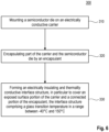
- Fig. 6 shows a flow diagram for illustrating a method for fabricating a semiconductor device package.
- the method 330 of Fig. 6 comprises mounting a semiconductor die on an electrically conductive carrier (310), encapsulating part of the carrier and the semiconductor die by an encapsulant (320), and forming an electrically insulating and thermally conductive interface structure, in particular to cover an exposed surface portion of the carrier and a connected surface portion of the encapsulant, the interface structure comprising a glass transition temperature Tg in a range between -40°C to 150°C (330).
- the lower bound of the range of the temperature Tg can also be -30°C, -20°C, -10°C, 0°C, 10°C, 20°C, or 30°C
- the upper bound of the range can also be 140°C, 130°C, 120°C, 110°C, 100°C, 90°C, 80°C, 70°C, 60°C, 50°C, or 40°C.
Landscapes
- Cooling Or The Like Of Semiconductors Or Solid State Devices (AREA)
- Engineering & Computer Science (AREA)
- Chemical & Material Sciences (AREA)
- Materials Engineering (AREA)
- Ceramic Engineering (AREA)
- Microelectronics & Electronic Packaging (AREA)
Claims (9)
- Halbleiterbauelementpaket (100) umfassend:einen elektrisch leitfähigen Träger (10);einen auf dem Träger (10) angeordneten Halbleiterchip (20);ein Verkapselungsmittel (40), das einen Teil des Trägers (10) und des Halbleiterchips (20) verkapselt;eine elektrisch isolierende und wärmeleitende Schnittstellenstruktur (30), die einen freiliegenden Oberflächenabschnitt des Trägers (10) und einen verbundenen Oberflächenabschnitts des Verkapselungsmittels (40) bedeckt;wobei die Schnittstellenstruktur (30) eine Glasübergangstemperatur in einem Bereich zwischen -40°C bis 150 °C aufweist,dadurch gekennzeichnet, dassdie Schnittstellenstruktur (30) bei einer Temperatur von 100 °C eine Härte in einem Bereich zwischen 10 MPa und 100 MPa aufweist.
- Halbleiterbauelementpaket (100) nach Anspruch 1, wobei
die Schnittstellenstruktur (30) ein Harzmaterial, insbesondere ein Epoxidharzmaterial umfasst. - Halbleiterbauelementpaket (100) nach Anspruch 2, wobei
die Schnittstellenstruktur (30) eine Harzmatrix umfasst, die mit Füllstoffpartikeln gefüllt ist, insbesondere Füllstoffpartikeln, die mindestens eines aus der Gruppe bestehend aus Metalloxid, Metallnitrid, Aluminiumoxid, Siliciumoxid, Bornitrid, Zirkoniumoxid, Siliciumnitrid, Diamant und Aluminiumnitrid umfassen. - Halbleiterbauelementpaket (100) nach Anspruch 3, wobei
ein Massenprozentsatz der Füllstoffpartikel in einem Bereich zwischen 75 % und 98 % liegt. - Halbleiterbauelementpaket (100) nach einem der vorhergehenden Ansprüche, wobei
die Schnittstellenstruktur (30) bei einer Temperatur von 22 °C eine Härte in einem Bereich zwischen 50 MPa und 500 MPa aufweist. - Halbleiterbauelementpaket (100) nach einem der vorhergehenden Ansprüche, wobei
die Schnittstellenstruktur (30) eine Dicke in einem Bereich zwischen 50 µm und 1000 µm aufweist. - Halbleiterbauelementpaket (100) nach einem der vorhergehenden Ansprüche, wobei
der Träger (10) eines oder mehrere von einem Abschnitt eines Leiterrahmens, einer Direct Copper Bond (DCB), einem Active Metal Braze (AMB) und/oder einem isolierten Metallsubstrat (IMS) ist. - Halbleiterbauelementpaket (100) nach einem der vorhergehenden Ansprüche, wobei
der Halbleiterchip (20) einen oder mehrere von einem vertikalen Transistorchip, einem MOSFET-Chip, einem IGBT-Chip, einem SiC-MOS-Chip, einem Cool-MOS-Chip, einem S-FET-Chip, einem Gate-Treiberchip, einer Steuerung oder einem Konnektivitätschip oder einem Abfühlchip umfasst. - Halbleiterbauelementpaket (100) nach einem der vorhergehenden Ansprüche, wobei
das Halbleiterbauelementpaket (100) eines oder mehrere von einem diskreten oder standardisierten Paket, einem diskreten oder standardisierten Leistungspaket, einem TO-Paket, einem TO220-Paket, einem TO247-Paket, einem TO263-Paket, einem D2PAK-Paket, einem Oberseiten-Kühlpaket, einem Leistungsmodul oder einem intelligenten Leistungsmodul ist.
Priority Applications (3)
| Application Number | Priority Date | Filing Date | Title |
|---|---|---|---|
| EP20185063.3A EP3937227B1 (de) | 2020-07-09 | 2020-07-09 | Halbleiterbauelementpaket mit einem thermischen schnittstellenmaterial mit verbesserten handhabungseigenschaften |
| US17/368,311 US12237242B2 (en) | 2020-07-09 | 2021-07-06 | Semiconductor device package comprising a thermal interface material with improved handling properties |
| CN202110781575.1A CN113921484B (zh) | 2020-07-09 | 2021-07-08 | 包括具有改进的处理特性的热界面材料的半导体器件封装 |
Applications Claiming Priority (1)
| Application Number | Priority Date | Filing Date | Title |
|---|---|---|---|
| EP20185063.3A EP3937227B1 (de) | 2020-07-09 | 2020-07-09 | Halbleiterbauelementpaket mit einem thermischen schnittstellenmaterial mit verbesserten handhabungseigenschaften |
Publications (3)
| Publication Number | Publication Date |
|---|---|
| EP3937227A1 EP3937227A1 (de) | 2022-01-12 |
| EP3937227A9 EP3937227A9 (de) | 2022-03-02 |
| EP3937227B1 true EP3937227B1 (de) | 2025-03-05 |
Family
ID=71607703
Family Applications (1)
| Application Number | Title | Priority Date | Filing Date |
|---|---|---|---|
| EP20185063.3A Active EP3937227B1 (de) | 2020-07-09 | 2020-07-09 | Halbleiterbauelementpaket mit einem thermischen schnittstellenmaterial mit verbesserten handhabungseigenschaften |
Country Status (3)
| Country | Link |
|---|---|
| US (1) | US12237242B2 (de) |
| EP (1) | EP3937227B1 (de) |
| CN (1) | CN113921484B (de) |
Families Citing this family (1)
| Publication number | Priority date | Publication date | Assignee | Title |
|---|---|---|---|---|
| EP3518278A1 (de) * | 2018-01-30 | 2019-07-31 | Infineon Technologies AG | Leistungshalbleitermodul und verfahren zur dessen herstellung |
Family Cites Families (4)
| Publication number | Priority date | Publication date | Assignee | Title |
|---|---|---|---|---|
| MY112145A (en) * | 1994-07-11 | 2001-04-30 | Ibm | Direct attachment of heat sink attached directly to flip chip using flexible epoxy |
| CN105659711A (zh) * | 2013-10-17 | 2016-06-08 | 住友电木株式会社 | 环氧树脂组合物、带有树脂层的载体材料、金属基电路基板和电子装置 |
| US9847509B2 (en) * | 2015-01-22 | 2017-12-19 | Industrial Technology Research Institute | Package of flexible environmental sensitive electronic device and sealing member |
| DE102015118245B4 (de) * | 2015-10-26 | 2024-10-10 | Infineon Technologies Austria Ag | Elektronische Komponente mit einem thermischen Schnittstellenmaterial, Herstellungsverfahren für eine elektronische Komponente, Wärmeabfuhrkörper mit einem thermischen Schnittstellenmaterial und thermisches Schnittstellenmaterial |
-
2020
- 2020-07-09 EP EP20185063.3A patent/EP3937227B1/de active Active
-
2021
- 2021-07-06 US US17/368,311 patent/US12237242B2/en active Active
- 2021-07-08 CN CN202110781575.1A patent/CN113921484B/zh active Active
Also Published As
| Publication number | Publication date |
|---|---|
| EP3937227A1 (de) | 2022-01-12 |
| CN113921484A (zh) | 2022-01-11 |
| US12237242B2 (en) | 2025-02-25 |
| US20220013433A1 (en) | 2022-01-13 |
| CN113921484B (zh) | 2026-03-20 |
| EP3937227A9 (de) | 2022-03-02 |
Similar Documents
| Publication | Publication Date | Title |
|---|---|---|
| US20210020541A1 (en) | Thermal interface material having defined thermal, mechanical and electric properties | |
| US10283432B2 (en) | Molded package with chip carrier comprising brazed electrically conductive layers | |
| US11862533B2 (en) | Fluid-cooled package having shielding layer | |
| US9922910B2 (en) | Functionalized interface structure | |
| US10615097B2 (en) | Chip carrier with electrically conductive layer extending beyond thermally conductive dielectric sheet | |
| CN103928411B (zh) | 芯片装置及其制造方法、集成电路及其制造方法 | |
| US11251112B2 (en) | Dual side cooling power module and manufacturing method of the same | |
| US11626351B2 (en) | Semiconductor package with barrier to contain thermal interface material | |
| EP4170708B1 (de) | Elektronisches modul mit einem halbleitergehäuse mit integriertem clip und befestigungselement | |
| US10854547B2 (en) | Chip package with cross-linked thermoplastic dielectric | |
| CN108346651A (zh) | 包括晶体管芯片、二极管芯片和驱动器芯片的半导体模块 | |
| CN108695286B (zh) | 具有经由间隔颗粒与载体连接的构件的封装体 | |
| JP2015211178A (ja) | 半導体装置 | |
| US12237242B2 (en) | Semiconductor device package comprising a thermal interface material with improved handling properties | |
| US20220293484A1 (en) | Integrated circuit package system | |
| CN117790434A (zh) | 在电子部件的顶部具有电绝缘导热层的封装体 | |
| CN116722002A (zh) | 半导体封装和包括半导体封装的半导体装置模块 | |
| KR101204223B1 (ko) | 전력 모듈 패키지 및 그 제조방법 | |
| US20250157869A1 (en) | Encapsulant with organic constituent and inorganic constituent having adjusted relative dielectric constant | |
| US20250218914A1 (en) | Package with component-carrying intermediate structure and additional carrier having reference potential structure | |
| US20250266310A1 (en) | Encapsulant with low cte and low young modulus for low-stress electronic package |
Legal Events
| Date | Code | Title | Description |
|---|---|---|---|
| PUAI | Public reference made under article 153(3) epc to a published international application that has entered the european phase |
Free format text: ORIGINAL CODE: 0009012 |
|
| STAA | Information on the status of an ep patent application or granted ep patent |
Free format text: STATUS: THE APPLICATION HAS BEEN PUBLISHED |
|
| AK | Designated contracting states |
Kind code of ref document: A1 Designated state(s): AL AT BE BG CH CY CZ DE DK EE ES FI FR GB GR HR HU IE IS IT LI LT LU LV MC MK MT NL NO PL PT RO RS SE SI SK SM TR |
|
| B565 | Issuance of search results under rule 164(2) epc |
Effective date: 20201127 |
|
| STAA | Information on the status of an ep patent application or granted ep patent |
Free format text: STATUS: REQUEST FOR EXAMINATION WAS MADE |
|
| 17P | Request for examination filed |
Effective date: 20220602 |
|
| RBV | Designated contracting states (corrected) |
Designated state(s): AL AT BE BG CH CY CZ DE DK EE ES FI FR GB GR HR HU IE IS IT LI LT LU LV MC MK MT NL NO PL PT RO RS SE SI SK SM TR |
|
| STAA | Information on the status of an ep patent application or granted ep patent |
Free format text: STATUS: EXAMINATION IS IN PROGRESS |
|
| 17Q | First examination report despatched |
Effective date: 20240710 |
|
| GRAP | Despatch of communication of intention to grant a patent |
Free format text: ORIGINAL CODE: EPIDOSNIGR1 |
|
| STAA | Information on the status of an ep patent application or granted ep patent |
Free format text: STATUS: GRANT OF PATENT IS INTENDED |
|
| RIC1 | Information provided on ipc code assigned before grant |
Ipc: H01L 23/495 20060101ALN20241010BHEP Ipc: H01L 23/433 20060101ALN20241010BHEP Ipc: H01L 23/373 20060101AFI20241010BHEP |
|
| RIC1 | Information provided on ipc code assigned before grant |
Ipc: H01L 23/495 20060101ALN20241014BHEP Ipc: H01L 23/433 20060101ALN20241014BHEP Ipc: H01L 23/373 20060101AFI20241014BHEP |
|
| INTG | Intention to grant announced |
Effective date: 20241023 |
|
| GRAS | Grant fee paid |
Free format text: ORIGINAL CODE: EPIDOSNIGR3 |
|
| GRAA | (expected) grant |
Free format text: ORIGINAL CODE: 0009210 |
|
| STAA | Information on the status of an ep patent application or granted ep patent |
Free format text: STATUS: THE PATENT HAS BEEN GRANTED |
|
| P01 | Opt-out of the competence of the unified patent court (upc) registered |
Free format text: CASE NUMBER: APP_84/2025 Effective date: 20250102 |
|
| AK | Designated contracting states |
Kind code of ref document: B1 Designated state(s): AL AT BE BG CH CY CZ DE DK EE ES FI FR GB GR HR HU IE IS IT LI LT LU LV MC MK MT NL NO PL PT RO RS SE SI SK SM TR |
|
| REG | Reference to a national code |
Ref country code: GB Ref legal event code: FG4D |
|
| REG | Reference to a national code |
Ref country code: CH Ref legal event code: EP |
|
| REG | Reference to a national code |
Ref country code: DE Ref legal event code: R096 Ref document number: 602020047098 Country of ref document: DE |
|
| REG | Reference to a national code |
Ref country code: IE Ref legal event code: FG4D |
|
| PG25 | Lapsed in a contracting state [announced via postgrant information from national office to epo] |
Ref country code: RS Free format text: LAPSE BECAUSE OF FAILURE TO SUBMIT A TRANSLATION OF THE DESCRIPTION OR TO PAY THE FEE WITHIN THE PRESCRIBED TIME-LIMIT Effective date: 20250605 |
|
| PG25 | Lapsed in a contracting state [announced via postgrant information from national office to epo] |
Ref country code: FI Free format text: LAPSE BECAUSE OF FAILURE TO SUBMIT A TRANSLATION OF THE DESCRIPTION OR TO PAY THE FEE WITHIN THE PRESCRIBED TIME-LIMIT Effective date: 20250305 |
|
| REG | Reference to a national code |
Ref country code: NL Ref legal event code: MP Effective date: 20250305 |
|
| PG25 | Lapsed in a contracting state [announced via postgrant information from national office to epo] |
Ref country code: ES Free format text: LAPSE BECAUSE OF FAILURE TO SUBMIT A TRANSLATION OF THE DESCRIPTION OR TO PAY THE FEE WITHIN THE PRESCRIBED TIME-LIMIT Effective date: 20250305 |
|
| REG | Reference to a national code |
Ref country code: LT Ref legal event code: MG9D |
|
| PG25 | Lapsed in a contracting state [announced via postgrant information from national office to epo] |
Ref country code: NO Free format text: LAPSE BECAUSE OF FAILURE TO SUBMIT A TRANSLATION OF THE DESCRIPTION OR TO PAY THE FEE WITHIN THE PRESCRIBED TIME-LIMIT Effective date: 20250605 |
|
| PG25 | Lapsed in a contracting state [announced via postgrant information from national office to epo] |
Ref country code: HR Free format text: LAPSE BECAUSE OF FAILURE TO SUBMIT A TRANSLATION OF THE DESCRIPTION OR TO PAY THE FEE WITHIN THE PRESCRIBED TIME-LIMIT Effective date: 20250305 |
|
| PG25 | Lapsed in a contracting state [announced via postgrant information from national office to epo] |
Ref country code: LV Free format text: LAPSE BECAUSE OF FAILURE TO SUBMIT A TRANSLATION OF THE DESCRIPTION OR TO PAY THE FEE WITHIN THE PRESCRIBED TIME-LIMIT Effective date: 20250305 |
|
| PG25 | Lapsed in a contracting state [announced via postgrant information from national office to epo] |
Ref country code: GR Free format text: LAPSE BECAUSE OF FAILURE TO SUBMIT A TRANSLATION OF THE DESCRIPTION OR TO PAY THE FEE WITHIN THE PRESCRIBED TIME-LIMIT Effective date: 20250606 Ref country code: BG Free format text: LAPSE BECAUSE OF FAILURE TO SUBMIT A TRANSLATION OF THE DESCRIPTION OR TO PAY THE FEE WITHIN THE PRESCRIBED TIME-LIMIT Effective date: 20250305 |
|
| REG | Reference to a national code |
Ref country code: AT Ref legal event code: MK05 Ref document number: 1773768 Country of ref document: AT Kind code of ref document: T Effective date: 20250305 |
|
| PG25 | Lapsed in a contracting state [announced via postgrant information from national office to epo] |
Ref country code: NL Free format text: LAPSE BECAUSE OF FAILURE TO SUBMIT A TRANSLATION OF THE DESCRIPTION OR TO PAY THE FEE WITHIN THE PRESCRIBED TIME-LIMIT Effective date: 20250305 |
|
| PG25 | Lapsed in a contracting state [announced via postgrant information from national office to epo] |
Ref country code: SE Free format text: LAPSE BECAUSE OF FAILURE TO SUBMIT A TRANSLATION OF THE DESCRIPTION OR TO PAY THE FEE WITHIN THE PRESCRIBED TIME-LIMIT Effective date: 20250305 |
|
| PG25 | Lapsed in a contracting state [announced via postgrant information from national office to epo] |
Ref country code: SM Free format text: LAPSE BECAUSE OF FAILURE TO SUBMIT A TRANSLATION OF THE DESCRIPTION OR TO PAY THE FEE WITHIN THE PRESCRIBED TIME-LIMIT Effective date: 20250305 |
|
| PG25 | Lapsed in a contracting state [announced via postgrant information from national office to epo] |
Ref country code: PT Free format text: LAPSE BECAUSE OF FAILURE TO SUBMIT A TRANSLATION OF THE DESCRIPTION OR TO PAY THE FEE WITHIN THE PRESCRIBED TIME-LIMIT Effective date: 20250707 |
|
| PGFP | Annual fee paid to national office [announced via postgrant information from national office to epo] |
Ref country code: DE Payment date: 20250915 Year of fee payment: 6 |
|
| PG25 | Lapsed in a contracting state [announced via postgrant information from national office to epo] |
Ref country code: IT Free format text: LAPSE BECAUSE OF FAILURE TO SUBMIT A TRANSLATION OF THE DESCRIPTION OR TO PAY THE FEE WITHIN THE PRESCRIBED TIME-LIMIT Effective date: 20250305 Ref country code: PL Free format text: LAPSE BECAUSE OF FAILURE TO SUBMIT A TRANSLATION OF THE DESCRIPTION OR TO PAY THE FEE WITHIN THE PRESCRIBED TIME-LIMIT Effective date: 20250305 |
|
| PG25 | Lapsed in a contracting state [announced via postgrant information from national office to epo] |
Ref country code: AT Free format text: LAPSE BECAUSE OF FAILURE TO SUBMIT A TRANSLATION OF THE DESCRIPTION OR TO PAY THE FEE WITHIN THE PRESCRIBED TIME-LIMIT Effective date: 20250305 |
|
| PG25 | Lapsed in a contracting state [announced via postgrant information from national office to epo] |
Ref country code: CZ Free format text: LAPSE BECAUSE OF FAILURE TO SUBMIT A TRANSLATION OF THE DESCRIPTION OR TO PAY THE FEE WITHIN THE PRESCRIBED TIME-LIMIT Effective date: 20250305 Ref country code: EE Free format text: LAPSE BECAUSE OF FAILURE TO SUBMIT A TRANSLATION OF THE DESCRIPTION OR TO PAY THE FEE WITHIN THE PRESCRIBED TIME-LIMIT Effective date: 20250305 |
|
| PG25 | Lapsed in a contracting state [announced via postgrant information from national office to epo] |
Ref country code: RO Free format text: LAPSE BECAUSE OF FAILURE TO SUBMIT A TRANSLATION OF THE DESCRIPTION OR TO PAY THE FEE WITHIN THE PRESCRIBED TIME-LIMIT Effective date: 20250305 |
|
| PG25 | Lapsed in a contracting state [announced via postgrant information from national office to epo] |
Ref country code: SK Free format text: LAPSE BECAUSE OF FAILURE TO SUBMIT A TRANSLATION OF THE DESCRIPTION OR TO PAY THE FEE WITHIN THE PRESCRIBED TIME-LIMIT Effective date: 20250305 |
|
| PG25 | Lapsed in a contracting state [announced via postgrant information from national office to epo] |
Ref country code: IS Free format text: LAPSE BECAUSE OF FAILURE TO SUBMIT A TRANSLATION OF THE DESCRIPTION OR TO PAY THE FEE WITHIN THE PRESCRIBED TIME-LIMIT Effective date: 20250705 |
|
| REG | Reference to a national code |
Ref country code: DE Ref legal event code: R079 Ref document number: 602020047098 Country of ref document: DE Free format text: PREVIOUS MAIN CLASS: H01L0023373000 Ipc: H10W0040250000 |
|
| REG | Reference to a national code |
Ref country code: DE Ref legal event code: R097 Ref document number: 602020047098 Country of ref document: DE |
|
| PLBE | No opposition filed within time limit |
Free format text: ORIGINAL CODE: 0009261 |
|
| STAA | Information on the status of an ep patent application or granted ep patent |
Free format text: STATUS: NO OPPOSITION FILED WITHIN TIME LIMIT |
|
| PG25 | Lapsed in a contracting state [announced via postgrant information from national office to epo] |
Ref country code: DK Free format text: LAPSE BECAUSE OF FAILURE TO SUBMIT A TRANSLATION OF THE DESCRIPTION OR TO PAY THE FEE WITHIN THE PRESCRIBED TIME-LIMIT Effective date: 20250305 |
|
| REG | Reference to a national code |
Ref country code: CH Ref legal event code: L10 Free format text: ST27 STATUS EVENT CODE: U-0-0-L10-L00 (AS PROVIDED BY THE NATIONAL OFFICE) Effective date: 20260114 |
|
| 26N | No opposition filed |
Effective date: 20251208 |
|
| REG | Reference to a national code |
Ref country code: CH Ref legal event code: H13 Free format text: ST27 STATUS EVENT CODE: U-0-0-H10-H13 (AS PROVIDED BY THE NATIONAL OFFICE) Effective date: 20260224 |
|
| PG25 | Lapsed in a contracting state [announced via postgrant information from national office to epo] |
Ref country code: LU Free format text: LAPSE BECAUSE OF NON-PAYMENT OF DUE FEES Effective date: 20250709 |
|
| GBPC | Gb: european patent ceased through non-payment of renewal fee |
Effective date: 20250709 |
|
| REG | Reference to a national code |
Ref country code: BE Ref legal event code: MM Effective date: 20250731 |
|
| PG25 | Lapsed in a contracting state [announced via postgrant information from national office to epo] |
Ref country code: GB Free format text: LAPSE BECAUSE OF NON-PAYMENT OF DUE FEES Effective date: 20250709 |
|
| PG25 | Lapsed in a contracting state [announced via postgrant information from national office to epo] |
Ref country code: BE Free format text: LAPSE BECAUSE OF NON-PAYMENT OF DUE FEES Effective date: 20250731 |
|
| PG25 | Lapsed in a contracting state [announced via postgrant information from national office to epo] |
Ref country code: FR Free format text: LAPSE BECAUSE OF NON-PAYMENT OF DUE FEES Effective date: 20250731 |
|
| PG25 | Lapsed in a contracting state [announced via postgrant information from national office to epo] |
Ref country code: CH Free format text: LAPSE BECAUSE OF NON-PAYMENT OF DUE FEES Effective date: 20250731 |