EP3937376B1 - Amplificateur en montage push-pull de classe e - Google Patents
Amplificateur en montage push-pull de classe e Download PDFInfo
- Publication number
- EP3937376B1 EP3937376B1 EP21184543.3A EP21184543A EP3937376B1 EP 3937376 B1 EP3937376 B1 EP 3937376B1 EP 21184543 A EP21184543 A EP 21184543A EP 3937376 B1 EP3937376 B1 EP 3937376B1
- Authority
- EP
- European Patent Office
- Prior art keywords
- line segment
- amplifier
- push
- class
- ground
- Prior art date
- Legal status (The legal status is an assumption and is not a legal conclusion. Google has not performed a legal analysis and makes no representation as to the accuracy of the status listed.)
- Active
Links
Images


Classifications
-
- H—ELECTRICITY
- H03—ELECTRONIC CIRCUITRY
- H03F—AMPLIFIERS
- H03F3/00—Amplifiers with only discharge tubes or only semiconductor devices as amplifying elements
- H03F3/20—Power amplifiers, e.g. Class B amplifiers, Class C amplifiers
- H03F3/21—Power amplifiers, e.g. Class B amplifiers, Class C amplifiers with semiconductor devices only
- H03F3/217—Class D power amplifiers; Switching amplifiers
- H03F3/2176—Class E amplifiers
-
- H—ELECTRICITY
- H03—ELECTRONIC CIRCUITRY
- H03F—AMPLIFIERS
- H03F1/00—Details of amplifiers with only discharge tubes, only semiconductor devices or only unspecified devices as amplifying elements
- H03F1/56—Modifications of input or output impedances, not otherwise provided for
-
- H—ELECTRICITY
- H03—ELECTRONIC CIRCUITRY
- H03F—AMPLIFIERS
- H03F3/00—Amplifiers with only discharge tubes or only semiconductor devices as amplifying elements
- H03F3/189—High-frequency amplifiers, e.g. radio frequency amplifiers
- H03F3/19—High-frequency amplifiers, e.g. radio frequency amplifiers with semiconductor devices only
- H03F3/195—High-frequency amplifiers, e.g. radio frequency amplifiers with semiconductor devices only in integrated circuits
-
- H—ELECTRICITY
- H03—ELECTRONIC CIRCUITRY
- H03F—AMPLIFIERS
- H03F3/00—Amplifiers with only discharge tubes or only semiconductor devices as amplifying elements
- H03F3/20—Power amplifiers, e.g. Class B amplifiers, Class C amplifiers
- H03F3/21—Power amplifiers, e.g. Class B amplifiers, Class C amplifiers with semiconductor devices only
- H03F3/213—Power amplifiers, e.g. Class B amplifiers, Class C amplifiers with semiconductor devices only in integrated circuits
-
- H—ELECTRICITY
- H03—ELECTRONIC CIRCUITRY
- H03F—AMPLIFIERS
- H03F3/00—Amplifiers with only discharge tubes or only semiconductor devices as amplifying elements
- H03F3/26—Push-pull amplifiers; Phase-splitters therefor
- H03F3/265—Push-pull amplifiers; Phase-splitters therefor with field-effect transistors only
-
- H—ELECTRICITY
- H03—ELECTRONIC CIRCUITRY
- H03F—AMPLIFIERS
- H03F3/00—Amplifiers with only discharge tubes or only semiconductor devices as amplifying elements
- H03F3/30—Single-ended push-pull [SEPP] amplifiers; Phase-splitters therefor
- H03F3/3001—Single-ended push-pull [SEPP] amplifiers; Phase-splitters therefor with field-effect transistors
-
- H—ELECTRICITY
- H03—ELECTRONIC CIRCUITRY
- H03F—AMPLIFIERS
- H03F3/00—Amplifiers with only discharge tubes or only semiconductor devices as amplifying elements
- H03F3/30—Single-ended push-pull [SEPP] amplifiers; Phase-splitters therefor
- H03F3/3001—Single-ended push-pull [SEPP] amplifiers; Phase-splitters therefor with field-effect transistors
- H03F3/3033—NMOS SEPP output stages
-
- H—ELECTRICITY
- H03—ELECTRONIC CIRCUITRY
- H03F—AMPLIFIERS
- H03F3/00—Amplifiers with only discharge tubes or only semiconductor devices as amplifying elements
- H03F3/60—Amplifiers in which coupling networks have distributed constants, e.g. with waveguide resonators
- H03F3/601—Amplifiers in which coupling networks have distributed constants, e.g. with waveguide resonators using FET's, e.g. GaAs FET's
-
- H—ELECTRICITY
- H03—ELECTRONIC CIRCUITRY
- H03F—AMPLIFIERS
- H03F2200/00—Indexing scheme relating to amplifiers
- H03F2200/06—A balun, i.e. balanced to or from unbalanced converter, being present at the input of an amplifier
-
- H—ELECTRICITY
- H03—ELECTRONIC CIRCUITRY
- H03F—AMPLIFIERS
- H03F2200/00—Indexing scheme relating to amplifiers
- H03F2200/09—A balun, i.e. balanced to or from unbalanced converter, being present at the output of an amplifier
-
- H—ELECTRICITY
- H03—ELECTRONIC CIRCUITRY
- H03F—AMPLIFIERS
- H03F2200/00—Indexing scheme relating to amplifiers
- H03F2200/21—Bias resistors are added at the input of an amplifier
-
- H—ELECTRICITY
- H03—ELECTRONIC CIRCUITRY
- H03F—AMPLIFIERS
- H03F2200/00—Indexing scheme relating to amplifiers
- H03F2200/297—Indexing scheme relating to amplifiers the loading circuit of an amplifying stage comprising a capacitor
-
- H—ELECTRICITY
- H03—ELECTRONIC CIRCUITRY
- H03F—AMPLIFIERS
- H03F2200/00—Indexing scheme relating to amplifiers
- H03F2200/315—Indexing scheme relating to amplifiers the loading circuit of an amplifying stage comprising a transmission line
-
- H—ELECTRICITY
- H03—ELECTRONIC CIRCUITRY
- H03F—AMPLIFIERS
- H03F2200/00—Indexing scheme relating to amplifiers
- H03F2200/387—A circuit being added at the output of an amplifier to adapt the output impedance of the amplifier
-
- H—ELECTRICITY
- H03—ELECTRONIC CIRCUITRY
- H03F—AMPLIFIERS
- H03F2200/00—Indexing scheme relating to amplifiers
- H03F2200/451—Indexing scheme relating to amplifiers the amplifier being a radio frequency amplifier
-
- H—ELECTRICITY
- H03—ELECTRONIC CIRCUITRY
- H03F—AMPLIFIERS
- H03F2200/00—Indexing scheme relating to amplifiers
- H03F2200/534—Transformer coupled at the input of an amplifier
-
- H—ELECTRICITY
- H03—ELECTRONIC CIRCUITRY
- H03F—AMPLIFIERS
- H03F2200/00—Indexing scheme relating to amplifiers
- H03F2200/541—Transformer coupled at the output of an amplifier
Definitions
- the present invention relates to a push-pull class E amplifier. Furthermore, the present invention relates to a device comprising such a push-pull solid state amplifier for industrial, scientific and medical applications like RF heating, drying and defrosting, and magnetic resonance imaging. Such device could for example be incorporated in plasma generation devices, laser systems, and particle accelerators.
- a push-pull amplifier typically comprises a first amplifying unit having a first input and a first output, and a second amplifying unit having a second input and a second output.
- the first and second amplifying units are driven with a 180 degrees phase offset relative to each other.
- a signal received at an input of the amplifier is distributed to the first input and the second input with a 180 degrees phase difference.
- the input of the amplifier is unbalanced, and a balun is used for transforming the unbalanced input signal into balanced signals that are fed to the first and second inputs.
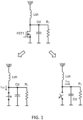
- a class E amplifier is an amplifier in which the transistor is used as a switch.
- Figure 1 illustrates the operational principles of a class E amplifier.
- the drain of a field-effect transistor FET1 is connected to a radiofrequency ⁇ RF' choke Lch through which a DC bias Vdd is provided. Furthermore, the drain is connected to shunt capacitor Cd and load R L .
- FET1 The gate of FET1 is driven such that FET1 is either fully opened, shown in the bottom right figure, or fully closed, shown in the bottom left figure.
- a current Ids flows through Lch and through FET1.
- the voltage over Cd is preferably as low as possible.
- FET1 is opened, the stored magnetic energy is released from Lch through a current Ids that flows through Cd and R L .
- the voltage over Cd is preferably very low and the cycle may be repeated.
- the overlap in time between a current flowing through FET1 and a drain-source voltage being larger than 0V can be limited thereby reducing power consumption inside FET1 and improving efficiency.
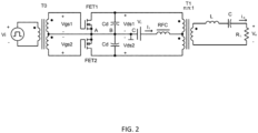
- Push-pull class E amplifiers are known in the art. An example thereof is shown in figure 2 .
- the amplifier comprises an input transformer T0 by which an unbalanced signal V i received at the input is distributed as a balanced signal over the inputs of the field-effect transistors FET1, FET2, where it is supplied as gate-source voltages V gs1 and V gs2 .
- the sources of FET1 and FET2 are connected at node A.
- the drains of transistors FET1, FET2 are connected to capacitors Cd that are mutually connected at a node B. Instead of two capacitors Cd to ground, a single capacitor arranged in between the drains of FET1, FET2 could equally be used.
- the drain-source voltage of FET1, FET2 is indicated as V ds1 and V ds2 , respectively.
- each field-effect transistor FET1, FET2 is connected to a part of the primary side of a transformer T1.
- the secondary side of the transformer T1 is connected to a load R L via a series resonance circuit of a capacitor C and an inductor L.
- This latter resonance circuit is configured to resonate at a frequency within the operational frequency range of the amplifier. This circuit can be used to reject higher harmonics.
- Transistors FET1, FET2 are fed using a voltage source V 1 via a choke inductor RFC that is connected to a virtual ground point on the primary side of transformer T1. It is further noted that nodes A and B, which also act as virtual grounds, are connected to a physical ground at node C.
- the amplifier of figure 2 could be implemented on a printed circuit board that comprises a dielectric layer. More in particular, transformer T1 could be realized using a quarter wavelength balun. In this case, the primary side of transformer T1 could be formed using a first line segment having a first end connected to the output, e.g. drain, of FET1 and a second line segment having a first end connected to the output of FET2. The second ends of the first and second line segments would then be connected to each other. The first and second line segments could form a loop and could be arranged on a first side of the dielectric layer of the printed circuit board. Together with capacitors Cd, the first and second line segments would form part of a class E matching network.
- the secondary side of transformer T1 could be formed using a third line segment that is arranged on a side of the dielectric layer opposite to the first side.
- a first end of the third line segment could be connected to ground and the second end of the third line segment could be connected to load R L , either directly or via impedance matching and/or harmonics filtering stages.
- the third line segment could form a second loop comprising m turns.
- the first line segment, second line segment, and the third line segment could be formed using coupled transmission lines.
- the length of the third line segment corresponds to a quarter wavelength at a frequency lying within the operational frequency range of the amplifier. Moreover, the length of the first line segment and the length of the second line segment would then each correspond to an eighth of a wavelength divided by m at the frequency lying within the operational frequency range of the amplifier.
- the first and second line segments are not too narrow due to the excessive currents that may flow in them. Furthermore, under these conditions, the output impedance of transistors FET1, FET2 will be relatively low.
- the third line segment preferably comprises as much turns as possible. However, for most amplifiers, a space for such turns is limited so that only 2 or 3 turns can be used.
- a push-pull class E amplifier as defined in the pre-amble of claim 1 is known from US7714649B1 . Furthermore, US5644272A describes a high frequency balun using both distributed and discrete elements connected together in a multilayer dielectric substrate.
- a push-pull class E amplifier as defined in claim 1, which is characterized in that it comprises a printed circuit board comprising a first and second dielectric layer, a first line segment arranged on the first dielectric layer, the first line segment having a first end and a second end, the first end of the first line segment being coupled to the first output, a second line segment arranged on the first dielectric layer, the second line segment having a first end and a second end, the first end of the second line segment being coupled to the second output, and the second ends of the first and second line segments being connected to each other, the first and second line segments and the capacitive unit forming part of a class E matching network for the first and second amplifying units.
- the push-pull class E amplifier comprises a third line segment arranged in between the first and second dielectric layers and having a first and second end, wherein the first end is connected to ground, and a fourth line segment that is arranged on the second dielectric layer on a side facing away from the first dielectric layer and having a first end and a second end.
- the first end of the fourth line segment is connected to the second end of the third line segment through a via extending through the second dielectric layer, and the second end of the fourth line segment is connected to the output.
- a combined length of the third line segment and the fourth line segment equals a quarter wavelength at the frequency lying within the operational frequency range of the push-pull class E amplifier.
- the first and second line segments form a first loop
- the third line segment forms a second loop comprising m turns
- the fourth line segment forms a third loop comprising n turns.
- a length of the first line segment and a length of the second line segment each correspond to an eighth of a wavelength divided by (n+m) at the frequency lying within the operational frequency range of the amplifier.
- the first line segment, second line segment, and the third line segment are formed using coupled transmission lines.
- the third line segment and the fourth line segment are formed using coupled transmission lines. It is noted that the fourth line segment only has a very weak coupling to the first and second line segment due to the shielding of the third line segment.
- microstrip line or strip line technology could be used.
- adding a fourth line segment provides a substantial advantage. More in particular, the addition of the fourth line segment allows the first and second line segments to be shortened. This allows a higher capacitance value to be used for capacitors Cd, which in turn results in a higher output power.
- At least m or n can be greater than 1.
- both m and n may equal 2.
- the first and second line segments may occupy a first ring-shaped surface area on the first dielectric layer.
- the third line segment and the fourth line segment may occupy a second and third ring-shaped surface area, respectively, that, when projected onto the first surface area in a direction perpendicular to the printed circuit board, substantially fall within the first surface area.
- the first and second line segment may form a circular ring having an inner radius and an outer radius relative to a center of the ring.
- the third line segment and fourth line segment may each comprise one or more turns that extend around a respective center that is aligned in lateral direction with the center of the ring formed by the first and second line segments.
- the one or more turns of the third and fourth line segments extend in an area defined by the abovementioned inner and outer radius relative to the respective center.
- An inner and/or an outer perimeter of the first, second, and third ring-shaped areas may each have a square shape, a rectangular shape, a circular shape or oval shape.
- the push-pull class E amplifier may further comprise a first ground patch around which the first loop extends, a second ground patch around which the second loop extends, and a third ground patch around which the third loop extends, a surface area of the first, second, and third ground patches being substantially identical, and the first, second, and third ground patches being electrically connected using one or more vias extending through the first and/or second dielectric layers.
- the first, second, and third ground patches are aligned in the lateral direction.
- the push-pull class E amplifier may further comprise a first grounded surrounding area surrounding the first loop, a second grounded surrounding area surrounding the second loop, and a third ground surrounding area surrounding the third loop.
- the first, second, and third grounded surrounding areas are electrically connected to each other using one or more vias extending through the first and/or second dielectric layers.
- the first end of the third line segment can be physically and electrically connected to the second grounded surrounding area.
- the push-pull class E amplifier may further comprise one or more electrically isolating thermal bridges, each thermal bridge connecting the first or second line segment to the first ground patch or the first grounded surrounding area.
- thermal bridges may for instance be realized using a suitable ceramic material, such as aluminum nitride or beryllium oxide, and allow the first and second line segments, which carry the most current, to be sufficiently cooled.
- the turn(s) of the third line segment may run in the same direction around the second ground patch as the turn(s) of the fourth line segment around the third ground patch.
- the first amplifying unit and the second amplifying unit may each be comprised in a package that comprises a pair of separate and spaced apart connecting terminals, said connecting terminals being connected inside the package to the first and second outputs, respectively.
- the package can be mounted on the first dielectric layer.
- the connecting terminals may be in the form of leads.
- the package may comprise a first and second power transistor, each of the first and second power transistor being a silicon based laterally diffused metal-oxide-semiconductor , 'LDMOS', transistor, a vertical double-diffused metal-oxide semiconductor ,'VDMOS', transistor, or a gallium nitride based field-effect transistor, 'FET'.
- the first and second line segments can be capacitively coupled to ground at or near a point where they are connected. In this manner, the point at which they are connected can be RF shorted to ground without introducing a DC path to ground.
- Each of the first and second line segments can be connected to a respective biasing network for supplying DC current to the first and second amplifying units, respectively, wherein the biasing networks are part of the class E matching network.
- a single biasing network can be used for simultaneously biasing the first and second amplifying units.
- Such biasing network could be configured to provide DC current at or near a point where the first and second line segments are connected or another virtual ground point, for example as indicated by nodes A or B in figure 2 .
- the operational frequency range may lie in a range from 1 MHz to 200 MHz.
- a power of the outputted signal may lie in a range from 100W to 10kW.
- the present invention relates to a balun for transforming a balanced signal received at a first and second balanced terminal into an unbalanced signal outputted at an unbalanced terminal.
- the balun comprises a printed circuit board having a first dielectric layer and a second dielectric layer.
- the balun further comprises a first line segment having a first end and a second end, the first end of the first line segment being coupled to the first balanced terminal, and a second line segment having a first end and a second end, the first end of the second line segment being coupled to the second balanced terminal.
- the second ends of the first and second line segments are connected to each other, and the first line segment and the second line segment are arranged on the first dielectric layer.
- the first and second line segments form a first loop.
- the balun further comprises a third line segment arranged in between the first and second dielectric layers and having a first and second end, wherein the first end is connected to ground.
- the third line segment forms a second loop comprising m turns.
- the balun comprises a fourth line segment arranged on the second dielectric layer on a side facing away from the first dielectric layer and having a first end and a second end, the first end of the fourth line segment being connected to the second end of the third line segment through a via extending through the second dielectric layer, and the second end of the fourth line segment being connected to the unbalanced terminal.
- the fourth line segment forms a third loop comprising n turns.
- a combined length of the third line segment and the fourth line segment corresponds to a quarter wavelength at a frequency lying within an operational frequency range of the balun.
- a length of the first line segment and a length of the second line segment each corresponds to an eighth of a wavelength divided by (n+m) at the frequency lying within the operational frequency range of the amplifier.
- the first line segment, second line segment, and the third line segment are formed using coupled transmission lines, and the third line segment and the fourth line segment are formed using coupled transmission lines.
- the present invention provides an electronic device comprising the abovementioned push-pull class E amplifier or balun.
- FIG 3 illustrates an embodiment of a push-pull class E amplifier according to the invention.
- the electrical equivalent of this amplifier is shown in figure 4 .
- a package 100 is shown in which two LDMOS power transistors are arranged, FET1 and FET2, although GaN FETs, VDMOS transistors, or a combination thereof could equally be used.
- An equivalent circuit of package 100 is shown in figure 4 .
- Each of the transistors has its own output lead 101A, 101B and input lead 102A, 102B, which are connected to a metal layer on a first dielectric layer of a printed circuit board 150.
- the upper transistor is connected to a first line segment W1A and the lower transistor to a second line segment W1B. These segments form a first loop around a ground patch 104. Other than ground patch 104, grounded surrounding areas 105 are provided.
- the point where line segments W1A, W1B are physically connected is RF shorted using capacitors C15, C16, C17.
- thermal bridges QB1-QB8 are provided to ensure proper cooling of line segments W1A, W1B during operation.
- Biasing networks B1 and B2 are used for supplying DC power to the output of the power transistors.
- biasing network B1 comprises resistors R6, R7, inductors L5, L7, and capacitors C5, C8, C11, C13.
- biasing network B2 comprises resistors R5, R8, inductors L6, L8, and capacitors C6, C9, C12, C14.
- biasing network B3 comprises resistors R1, R2, inductor L3, and capacitors C1, C3.
- biasing network B4 comprises resistors R3, R4, inductor L4, and capacitors C2, C4.
- a transformer network T3 is used for transforming the unbalanced signal received at the input RF IN to a balanced signal to be fed to the power transistors inside package 100.
- Figures 5 and 6 illustrate the inner metal layers of printed circuit board 150.
- a third line segment W2 is shown that at one end 111 is connected to a grounded surrounding area 112. The other end 113 is connected using a plurality of vias 114 to a fourth line segment W3 that is shown in figure 6 .
- Third line segment W2 makes two turns around a central ground patch 115 that is aligned with ground patch 104 and that is electrically connected thereto and to ground patch 124 using multiple vias 116.
- the area occupied by third line segment W2 roughly corresponds to the area occupied by first and second line segments W1A, W1B.
- fourth line segment W3 the same holds for fourth line segment W3.
- This latter segment has an end 121 connected to end 113 of third line segment W2 and an other end 122 to an output RF OUT of the amplifier using a plurality of vias 123 that extend through the first and second dielectric layers.
- Fourth line segment W3 makes two turns around a central ground patch 124, which patch is electrically connected to patches 115, 104 using vias 116.
- third line segment W2 and fourth line segment W3 each run clockwise around their respective ground patches 115, 124.
- present embodiments feature a third and a fourth line segment
- present invention equally relates to embodiments in which more line segments are realized in different metal layers.
Landscapes
- Engineering & Computer Science (AREA)
- Power Engineering (AREA)
- Microelectronics & Electronic Packaging (AREA)
- Amplifiers (AREA)
- Microwave Amplifiers (AREA)
Claims (15)
- Amplificateur en montage push-pull de classe E, comprenant :une entrée (RF IN) configurée pour la réception d'un signal devant être amplifié ;une sortie (RF OUT) configurée pour la sortie du signal après amplification ;une première unité d'amplification ayant une première entrée (102A) et une première sortie (101A) ;une seconde unité d'amplification ayant une seconde entrée (102B) et une seconde sortie (101B), la première et la seconde unité d'amplification étant configurées pour fonctionner en classe E ;un symétriseur ayant un port asymétrique connecté à l'entrée (RF IN), et un premier port symétrique connecté à la première entrée (102A) et un second port symétrique connecté à la seconde entrée (102B) ; etune unité capacitive comprenant soit un premier condensateur couplé entre la première sortie (101A) et une masse et un second condensateur entre la seconde sortie (101B) et la masse, soit un condensateur (C7 ; C10) couplé entre les première et seconde sorties (101A, 101B),caractérisé en ce quel'amplificateur en montage push-pull de classe E comprend en outre :une carte de circuit imprimé (150) ayant une première couche diélectrique et une seconde couche diélectrique ;un premier segment de ligne (W1A) agencé sur la première couche diélectrique, le premier segment de ligne (W1A) ayant une première extrémité et une seconde extrémité, la première extrémité du premier segment de ligne (W1A) étant couplée à la première sortie (101A) ;un deuxième segment de ligne (W1B) agencé sur la première couche diélectrique, le deuxième segment de ligne (W1B) ayant une première extrémité et une seconde extrémité, la première extrémité du deuxième segment de ligne (W1B) étant couplée à la seconde sortie (101B), et les secondes extrémités des premier et deuxième segments de ligne (W1A, W1B) étant connectées l'une à l'autre, les premier et deuxième segments de ligne (W1A, W1B) et l'unité capacitive faisant partie d'un réseau d'adaptation de classe E pour les première et seconde unités d'amplification ;un troisième segment de ligne (W2) agencé entre les première et seconde couches diélectriques et ayant une première et une seconde extrémité (111, 113), dans lequel la première extrémité (111) est connectée à la masse ; etun quatrième segment de ligne (W3) agencé sur la seconde couche diélectrique sur un côté tournant le dos à la première couche diélectrique et ayant une première extrémité (121) et une seconde extrémité (122), la première extrémité (121) du quatrième segment de ligne (W3) étant connectée à la seconde extrémité (113) du troisième segment de ligne (W2) par le biais d'un trou d'interconnexion (114) s'étendant à travers la seconde couche diélectrique, et la seconde extrémité (122) du quatrième segment de ligne (W3) étant connectée à la sortie (RF OUT),dans lequel une longueur combinée du troisième segment de ligne (W2) et du quatrième segment de ligne (W3) correspond à un quart de longueur d'onde à une fréquence se trouvant au sein d'une plage de fréquences fonctionnelle de l'amplificateur en montage push-pull de classe E,dans lequel les premier et deuxième segments de ligne (W1A, W1B) forment une première boucle,dans lequel le troisième segment de ligne (W2) forme une deuxième boucle comprenant m spires,dans lequel le quatrième segment de ligne (W3) forme une troisième boucle comprenant n spires,dans lequel une longueur du premier segment de ligne (W1A) et une longueur du deuxième segment de ligne (W1B) correspondent chacune à un huitième d'une longueur d'onde divisé par (n+m) à la fréquence se trouvant au sein de la plage de fréquences fonctionnelle de l'amplificateur en montage push-pull de classe E,dans lequel le premier segment de ligne (W1A), le deuxième segment de ligne (W1B) et le troisième segment de ligne (W2) sont formés à l'aide de lignes de transmission couplées, etdans lequel le troisième segment de ligne (W2) et le quatrième segment de ligne (W3) sont formés à l'aide de lignes de transmission couplées.
- Amplificateur en montage push-pull de classe E selon la revendication 1, dans lequel au moins m ou n est supérieur à 1.
- Amplificateur en montage push-pull de classe E selon la revendication 1 ou 2, dans lequel les premier et deuxième segments de ligne (W1A, W1B) occupent une première aire surfacique de forme annulaire sur la première couche diélectrique, et dans lequel le troisième segment de ligne (W2) et le quatrième segment de ligne (W3) occupent une deuxième et une troisième aire surfacique de forme annulaire, respectivement, qui, lorsqu'elles sont projetées sur la première aire surfacique dans une direction perpendiculaire à la carte de circuit imprimé, se retrouvent sensiblement au sein de la première aire surfacique, dans lequel un périmètre interne et/ou externe des première, deuxième et troisième aires de forme annulaire possèdent chacun une forme carrée, une forme rectangulaire, une forme circulaire ou une forme ovale.
- Amplificateur en montage push-pull de classe E selon la revendication 3, comprenant en outre un premier plot de masse (104) autour duquel la première boucle s'étend, un deuxième plot de masse (115) autour duquel la deuxième boucle s'étend, et un troisième plot de masse (124) autour duquel la troisième boucle s'étend, une aire surfacique des premier, deuxième et troisième plots de masse (104, 115, 124) étant sensiblement identique, et les premier, deuxième et troisième plots de masse (104, 115, 124) étant électriquement connectés à l'aide d'un ou de plusieurs trous d'interconnexion (116) s'étendant à travers les première et/ou seconde couches diélectriques.
- Amplificateur en montage push-pull de classe E selon la revendication 4, comprenant en outre une première aire d'encerclement mise à la masse (105) encerclant la première boucle, une deuxième aire d'encerclement mise à la masse (112) encerclant la deuxième boucle, et une troisième aire d'encerclement mise à la masse encerclant la troisième boucle, les première, deuxième et troisième aires d'encerclement mises à la masse étant électriquement connectés les unes aux autres à l'aide d'un ou de plusieurs trous d'interconnexion s'étendant à travers les première et/ou seconde couches diélectriques.
- Amplificateur en montage push-pull de classe E selon la revendication 5, dans lequel la première extrémité (111) du troisième segment de ligne (W2) est physiquement et électriquement connectée à la deuxième aire d'encerclement mise à la masse (112).
- Amplificateur en montage push-pull de classe E selon l'une quelconque des revendications 4 à 6, comprenant en outre un ou plusieurs ponts thermiques (QB1-QB8) électriquement isolants, chaque pont thermique connectant le premier ou le deuxième segment de ligne (W1A ; W1B) au premier plot de masse ou à la première aire d'encerclement mise à la masse.
- Amplificateur en montage push-pull de classe E selon l'une quelconque des revendications 4 à 7, dans lequel la ou les spire(s) du troisième segment de ligne (W2) s'enroulent dans la même direction autour du deuxième plot de masse (115) que la ou les spire(s) du quatrième segment de ligne (W3) autour du troisième plot de masse (124).
- Amplificateur en montage push-pull de classe E selon l'une quelconque des revendications précédentes, dans lequel la première unité d'amplification et la seconde unité d'amplification sont comprises dans un boîtier (100) qui comprend une paire de bornes de connexion séparées et espacées, lesdites bornes de connexion étant connectées à l'intérieur du boîtier (100) aux première et seconde sorties (101A, 101B), respectivement, le boîtier (100) étant monté sur la première couche diélectrique.
- Amplificateur en montage push-pull de classe E selon la revendication 9, dans lequel le boîtier (100) comprend un premier et un second transistor de puissance, chacun du premier et du second transistor de puissance étant un transistor à semi-conducteur à oxyde métallique à diffusion latérale, « LDMOS », à base de silicium, un transistor à semi-conducteur à oxyde métallique à diffusion double verticale, « VDMOS », ou un transistor à effet de champ, « FET », à base de nitrure de gallium.
- Amplificateur en montage push-pull de classe E selon l'une quelconque des revendications précédentes, dans lequel les premier et deuxième segments de ligne (W1A, W1B) sont couplés de manière capacitive à la masse au niveau ou près d'un point où ils sont connectés.
- Amplificateur en montage push-pull de classe E selon l'une quelconque des revendications précédentes, dans lequel chacun des premier et deuxième segments de ligne (W1A, W1B) est connecté à un réseau de polarisation respectif pour 1' alimentation, avec un courant continu, CC, des première et seconde unités d'amplification, respectivement, lesdits réseaux de polarisation faisant partie du réseau d'adaptation de classe E.
- Amplificateur en montage push-pull de classe E selon l'une quelconque des revendications 1 à 11, comprenant en outre un réseau de polarisation (B1, B2, B3, B4) pour l'alimentation, avec un courant CC, des première et seconde unités d'amplification au niveau ou près d'un point où les premier et deuxième segments de ligne (W1A, W1B) sont connectés.
- Amplificateur en montage push-pull de classe E selon l'une quelconque des revendications précédentes, dans lequel la plage de fréquences fonctionnelle se trouve dans une plage de 1 MHz à 200 MHz, et/ou dans lequel une puissance du signal délivré en sortie se trouve dans une plage de 100 W à 10 kW.
- Dispositif électronique comprenant l'amplificateur en montage push-pull de classe E selon l'une quelconque des revendications précédentes, dans lequel le dispositif électronique est l'un parmi un amplificateur à semi-conducteurs en montage push-pull pour des applications industrielles, scientifiques et médicales telles que le chauffage, le séchage et le dégivrage par radiofréquences, RF, et l'imagerie par résonance magnétique,
dans lequel le dispositif électronique est incorporé dans un dispositif de génération de plasma, un système laser et un accélérateur de particules.
Applications Claiming Priority (1)
| Application Number | Priority Date | Filing Date | Title |
|---|---|---|---|
| NL2026017A NL2026017B1 (en) | 2020-07-08 | 2020-07-08 | Push-pull class E amplifier |
Publications (2)
| Publication Number | Publication Date |
|---|---|
| EP3937376A1 EP3937376A1 (fr) | 2022-01-12 |
| EP3937376B1 true EP3937376B1 (fr) | 2023-09-06 |
Family
ID=72802095
Family Applications (1)
| Application Number | Title | Priority Date | Filing Date |
|---|---|---|---|
| EP21184543.3A Active EP3937376B1 (fr) | 2020-07-08 | 2021-07-08 | Amplificateur en montage push-pull de classe e |
Country Status (4)
| Country | Link |
|---|---|
| US (1) | US11545942B2 (fr) |
| EP (1) | EP3937376B1 (fr) |
| CN (1) | CN113922774B (fr) |
| NL (1) | NL2026017B1 (fr) |
Family Cites Families (9)
| Publication number | Priority date | Publication date | Assignee | Title |
|---|---|---|---|---|
| US5644272A (en) * | 1996-03-05 | 1997-07-01 | Telefonaktiebolaget Lm Ericsson | High frequency balun provided in a multilayer substrate |
| US7180758B2 (en) * | 1999-07-22 | 2007-02-20 | Mks Instruments, Inc. | Class E amplifier with inductive clamp |
| US7714649B1 (en) * | 2008-06-02 | 2010-05-11 | Rockwell Collins, Inc. | High-efficiency linear amplifier using non linear circuits |
| US8344801B2 (en) * | 2010-04-02 | 2013-01-01 | Mks Instruments, Inc. | Variable class characteristic amplifier |
| CN202261179U (zh) * | 2011-07-11 | 2012-05-30 | 成都信息工程学院 | 一种p波段射频推挽高功率放大器 |
| US9106204B2 (en) * | 2013-06-10 | 2015-08-11 | Avago Technologies General Ip (Singapore) Pte. Ltd. | Four LC element balun |
| DE102014213684B4 (de) * | 2014-07-15 | 2023-06-15 | Rohde & Schwarz GmbH & Co. Kommanditgesellschaft | Wirkungsgradoptimierter Hochfrequenzleistungsverstärker |
| CN107196609B (zh) * | 2017-05-31 | 2023-05-30 | 中国电子科技集团公司第十三研究所 | 石墨烯射频放大器 |
| CN209897013U (zh) * | 2019-05-07 | 2020-01-03 | 四川成电大为科技有限公司 | 一种基于GaN的射频E类互补推挽式放大器 |
-
2020
- 2020-07-08 NL NL2026017A patent/NL2026017B1/en not_active IP Right Cessation
-
2021
- 2021-07-07 US US17/369,572 patent/US11545942B2/en active Active
- 2021-07-07 CN CN202110767112.XA patent/CN113922774B/zh active Active
- 2021-07-08 EP EP21184543.3A patent/EP3937376B1/fr active Active
Also Published As
| Publication number | Publication date |
|---|---|
| US20220014159A1 (en) | 2022-01-13 |
| US11545942B2 (en) | 2023-01-03 |
| CN113922774B (zh) | 2025-07-18 |
| CN113922774A (zh) | 2022-01-11 |
| NL2026017B1 (en) | 2022-03-11 |
| EP3937376A1 (fr) | 2022-01-12 |
Similar Documents
| Publication | Publication Date | Title |
|---|---|---|
| JP4933598B2 (ja) | 分布型環状電力増幅器の構造 | |
| EP1601099B1 (fr) | Générateur RF à MOSFETs à commande de phase | |
| US8133347B2 (en) | Vacuum plasma generator | |
| US8581665B2 (en) | Doherty amplifier | |
| TW441165B (en) | Parallel HV MOSFET high power stable amplifier | |
| US8558619B2 (en) | Silicon-on-insulator high power amplifiers | |
| Park et al. | Millimeter-wave series power combining using sub-quarter-wavelength baluns | |
| JP7592747B2 (ja) | インピーダンス整合回路およびプラズマ給電システムおよび動作させるための方法 | |
| CN103856177B (zh) | 可变移相器、半导体集成电路和移相方法 | |
| US9450545B2 (en) | Dual-band semiconductor RF amplifier device | |
| CN110176909A (zh) | 功率放大器 | |
| JP2017533662A (ja) | 単一の直列キャパシタ及び分路キャパシタ構成要素を結合した出力整合ネットワーク | |
| US20240106396A1 (en) | Push-Pull Amplifying Unit and Doherty Amplifier Comprising the Same | |
| US10236841B2 (en) | Differential amplifier | |
| EP3937376B1 (fr) | Amplificateur en montage push-pull de classe e | |
| Mediano et al. | Class-E amplifiers and applications at MF, HF, and VHF | |
| EP3605842A1 (fr) | Balun et amplificateur comprenant le balun | |
| JP2008263432A (ja) | 分布型電力増幅器 | |
| Zhang et al. | A dual-band high-efficiency power amplifier based on novel impedance matching and harmonic control structure | |
| JPH08124685A (ja) | 電力増幅回路 | |
| WO2021199185A1 (fr) | Résonateur de type isolé, carte de circuit imprimé multicouche et appareil de transmission d'énergie sans fil | |
| JPH07154159A (ja) | 高周波増幅集積回路とそのドレインバイアス回路 |
Legal Events
| Date | Code | Title | Description |
|---|---|---|---|
| PUAI | Public reference made under article 153(3) epc to a published international application that has entered the european phase |
Free format text: ORIGINAL CODE: 0009012 |
|
| STAA | Information on the status of an ep patent application or granted ep patent |
Free format text: STATUS: THE APPLICATION HAS BEEN PUBLISHED |
|
| AK | Designated contracting states |
Kind code of ref document: A1 Designated state(s): AL AT BE BG CH CY CZ DE DK EE ES FI FR GB GR HR HU IE IS IT LI LT LU LV MC MK MT NL NO PL PT RO RS SE SI SK SM TR |
|
| B565 | Issuance of search results under rule 164(2) epc |
Effective date: 20210908 |
|
| STAA | Information on the status of an ep patent application or granted ep patent |
Free format text: STATUS: REQUEST FOR EXAMINATION WAS MADE |
|
| 17P | Request for examination filed |
Effective date: 20220712 |
|
| RBV | Designated contracting states (corrected) |
Designated state(s): AL AT BE BG CH CY CZ DE DK EE ES FI FR GB GR HR HU IE IS IT LI LT LU LV MC MK MT NL NO PL PT RO RS SE SI SK SM TR |
|
| GRAP | Despatch of communication of intention to grant a patent |
Free format text: ORIGINAL CODE: EPIDOSNIGR1 |
|
| STAA | Information on the status of an ep patent application or granted ep patent |
Free format text: STATUS: GRANT OF PATENT IS INTENDED |
|
| INTG | Intention to grant announced |
Effective date: 20230221 |
|
| GRAS | Grant fee paid |
Free format text: ORIGINAL CODE: EPIDOSNIGR3 |
|
| GRAA | (expected) grant |
Free format text: ORIGINAL CODE: 0009210 |
|
| STAA | Information on the status of an ep patent application or granted ep patent |
Free format text: STATUS: THE PATENT HAS BEEN GRANTED |
|
| AK | Designated contracting states |
Kind code of ref document: B1 Designated state(s): AL AT BE BG CH CY CZ DE DK EE ES FI FR GB GR HR HU IE IS IT LI LT LU LV MC MK MT NL NO PL PT RO RS SE SI SK SM TR |
|
| REG | Reference to a national code |
Ref country code: GB Ref legal event code: FG4D |
|
| REG | Reference to a national code |
Ref country code: CH Ref legal event code: EP |
|
| P01 | Opt-out of the competence of the unified patent court (upc) registered |
Effective date: 20230811 |
|
| REG | Reference to a national code |
Ref country code: NL Ref legal event code: FP Ref country code: IE Ref legal event code: FG4D |
|
| REG | Reference to a national code |
Ref country code: DE Ref legal event code: R096 Ref document number: 602021004881 Country of ref document: DE |
|
| REG | Reference to a national code |
Ref country code: LT Ref legal event code: MG9D |
|
| PG25 | Lapsed in a contracting state [announced via postgrant information from national office to epo] |
Ref country code: GR Free format text: LAPSE BECAUSE OF FAILURE TO SUBMIT A TRANSLATION OF THE DESCRIPTION OR TO PAY THE FEE WITHIN THE PRESCRIBED TIME-LIMIT Effective date: 20231207 |
|
| PG25 | Lapsed in a contracting state [announced via postgrant information from national office to epo] |
Ref country code: SE Free format text: LAPSE BECAUSE OF FAILURE TO SUBMIT A TRANSLATION OF THE DESCRIPTION OR TO PAY THE FEE WITHIN THE PRESCRIBED TIME-LIMIT Effective date: 20230906 Ref country code: RS Free format text: LAPSE BECAUSE OF FAILURE TO SUBMIT A TRANSLATION OF THE DESCRIPTION OR TO PAY THE FEE WITHIN THE PRESCRIBED TIME-LIMIT Effective date: 20230906 Ref country code: NO Free format text: LAPSE BECAUSE OF FAILURE TO SUBMIT A TRANSLATION OF THE DESCRIPTION OR TO PAY THE FEE WITHIN THE PRESCRIBED TIME-LIMIT Effective date: 20231206 Ref country code: LV Free format text: LAPSE BECAUSE OF FAILURE TO SUBMIT A TRANSLATION OF THE DESCRIPTION OR TO PAY THE FEE WITHIN THE PRESCRIBED TIME-LIMIT Effective date: 20230906 Ref country code: LT Free format text: LAPSE BECAUSE OF FAILURE TO SUBMIT A TRANSLATION OF THE DESCRIPTION OR TO PAY THE FEE WITHIN THE PRESCRIBED TIME-LIMIT Effective date: 20230906 Ref country code: HR Free format text: LAPSE BECAUSE OF FAILURE TO SUBMIT A TRANSLATION OF THE DESCRIPTION OR TO PAY THE FEE WITHIN THE PRESCRIBED TIME-LIMIT Effective date: 20230906 Ref country code: GR Free format text: LAPSE BECAUSE OF FAILURE TO SUBMIT A TRANSLATION OF THE DESCRIPTION OR TO PAY THE FEE WITHIN THE PRESCRIBED TIME-LIMIT Effective date: 20231207 Ref country code: FI Free format text: LAPSE BECAUSE OF FAILURE TO SUBMIT A TRANSLATION OF THE DESCRIPTION OR TO PAY THE FEE WITHIN THE PRESCRIBED TIME-LIMIT Effective date: 20230906 |
|
| REG | Reference to a national code |
Ref country code: AT Ref legal event code: MK05 Ref document number: 1609852 Country of ref document: AT Kind code of ref document: T Effective date: 20230906 |
|
| PG25 | Lapsed in a contracting state [announced via postgrant information from national office to epo] |
Ref country code: IS Free format text: LAPSE BECAUSE OF FAILURE TO SUBMIT A TRANSLATION OF THE DESCRIPTION OR TO PAY THE FEE WITHIN THE PRESCRIBED TIME-LIMIT Effective date: 20240106 |
|
| PG25 | Lapsed in a contracting state [announced via postgrant information from national office to epo] |
Ref country code: AT Free format text: LAPSE BECAUSE OF FAILURE TO SUBMIT A TRANSLATION OF THE DESCRIPTION OR TO PAY THE FEE WITHIN THE PRESCRIBED TIME-LIMIT Effective date: 20230906 |
|
| PG25 | Lapsed in a contracting state [announced via postgrant information from national office to epo] |
Ref country code: ES Free format text: LAPSE BECAUSE OF FAILURE TO SUBMIT A TRANSLATION OF THE DESCRIPTION OR TO PAY THE FEE WITHIN THE PRESCRIBED TIME-LIMIT Effective date: 20230906 |
|
| PG25 | Lapsed in a contracting state [announced via postgrant information from national office to epo] |
Ref country code: SM Free format text: LAPSE BECAUSE OF FAILURE TO SUBMIT A TRANSLATION OF THE DESCRIPTION OR TO PAY THE FEE WITHIN THE PRESCRIBED TIME-LIMIT Effective date: 20230906 Ref country code: RO Free format text: LAPSE BECAUSE OF FAILURE TO SUBMIT A TRANSLATION OF THE DESCRIPTION OR TO PAY THE FEE WITHIN THE PRESCRIBED TIME-LIMIT Effective date: 20230906 Ref country code: IS Free format text: LAPSE BECAUSE OF FAILURE TO SUBMIT A TRANSLATION OF THE DESCRIPTION OR TO PAY THE FEE WITHIN THE PRESCRIBED TIME-LIMIT Effective date: 20240106 Ref country code: ES Free format text: LAPSE BECAUSE OF FAILURE TO SUBMIT A TRANSLATION OF THE DESCRIPTION OR TO PAY THE FEE WITHIN THE PRESCRIBED TIME-LIMIT Effective date: 20230906 Ref country code: EE Free format text: LAPSE BECAUSE OF FAILURE TO SUBMIT A TRANSLATION OF THE DESCRIPTION OR TO PAY THE FEE WITHIN THE PRESCRIBED TIME-LIMIT Effective date: 20230906 Ref country code: CZ Free format text: LAPSE BECAUSE OF FAILURE TO SUBMIT A TRANSLATION OF THE DESCRIPTION OR TO PAY THE FEE WITHIN THE PRESCRIBED TIME-LIMIT Effective date: 20230906 Ref country code: AT Free format text: LAPSE BECAUSE OF FAILURE TO SUBMIT A TRANSLATION OF THE DESCRIPTION OR TO PAY THE FEE WITHIN THE PRESCRIBED TIME-LIMIT Effective date: 20230906 Ref country code: SK Free format text: LAPSE BECAUSE OF FAILURE TO SUBMIT A TRANSLATION OF THE DESCRIPTION OR TO PAY THE FEE WITHIN THE PRESCRIBED TIME-LIMIT Effective date: 20230906 Ref country code: PT Free format text: LAPSE BECAUSE OF FAILURE TO SUBMIT A TRANSLATION OF THE DESCRIPTION OR TO PAY THE FEE WITHIN THE PRESCRIBED TIME-LIMIT Effective date: 20240108 |
|
| PG25 | Lapsed in a contracting state [announced via postgrant information from national office to epo] |
Ref country code: PL Free format text: LAPSE BECAUSE OF FAILURE TO SUBMIT A TRANSLATION OF THE DESCRIPTION OR TO PAY THE FEE WITHIN THE PRESCRIBED TIME-LIMIT Effective date: 20230906 Ref country code: IT Free format text: LAPSE BECAUSE OF FAILURE TO SUBMIT A TRANSLATION OF THE DESCRIPTION OR TO PAY THE FEE WITHIN THE PRESCRIBED TIME-LIMIT Effective date: 20230906 |
|
| REG | Reference to a national code |
Ref country code: DE Ref legal event code: R097 Ref document number: 602021004881 Country of ref document: DE |
|
| PG25 | Lapsed in a contracting state [announced via postgrant information from national office to epo] |
Ref country code: DK Free format text: LAPSE BECAUSE OF FAILURE TO SUBMIT A TRANSLATION OF THE DESCRIPTION OR TO PAY THE FEE WITHIN THE PRESCRIBED TIME-LIMIT Effective date: 20230906 |
|
| PLBE | No opposition filed within time limit |
Free format text: ORIGINAL CODE: 0009261 |
|
| STAA | Information on the status of an ep patent application or granted ep patent |
Free format text: STATUS: NO OPPOSITION FILED WITHIN TIME LIMIT |
|
| PG25 | Lapsed in a contracting state [announced via postgrant information from national office to epo] |
Ref country code: DK Free format text: LAPSE BECAUSE OF FAILURE TO SUBMIT A TRANSLATION OF THE DESCRIPTION OR TO PAY THE FEE WITHIN THE PRESCRIBED TIME-LIMIT Effective date: 20230906 Ref country code: SI Free format text: LAPSE BECAUSE OF FAILURE TO SUBMIT A TRANSLATION OF THE DESCRIPTION OR TO PAY THE FEE WITHIN THE PRESCRIBED TIME-LIMIT Effective date: 20230906 |
|
| 26N | No opposition filed |
Effective date: 20240607 |
|
| PG25 | Lapsed in a contracting state [announced via postgrant information from national office to epo] |
Ref country code: BG Free format text: LAPSE BECAUSE OF FAILURE TO SUBMIT A TRANSLATION OF THE DESCRIPTION OR TO PAY THE FEE WITHIN THE PRESCRIBED TIME-LIMIT Effective date: 20230906 |
|
| PG25 | Lapsed in a contracting state [announced via postgrant information from national office to epo] |
Ref country code: BG Free format text: LAPSE BECAUSE OF FAILURE TO SUBMIT A TRANSLATION OF THE DESCRIPTION OR TO PAY THE FEE WITHIN THE PRESCRIBED TIME-LIMIT Effective date: 20230906 |
|
| PG25 | Lapsed in a contracting state [announced via postgrant information from national office to epo] |
Ref country code: MC Free format text: LAPSE BECAUSE OF FAILURE TO SUBMIT A TRANSLATION OF THE DESCRIPTION OR TO PAY THE FEE WITHIN THE PRESCRIBED TIME-LIMIT Effective date: 20230906 |
|
| REG | Reference to a national code |
Ref country code: CH Ref legal event code: PL |
|
| PG25 | Lapsed in a contracting state [announced via postgrant information from national office to epo] |
Ref country code: LU Free format text: LAPSE BECAUSE OF NON-PAYMENT OF DUE FEES Effective date: 20240708 |
|
| PG25 | Lapsed in a contracting state [announced via postgrant information from national office to epo] |
Ref country code: LU Free format text: LAPSE BECAUSE OF NON-PAYMENT OF DUE FEES Effective date: 20240708 |
|
| PG25 | Lapsed in a contracting state [announced via postgrant information from national office to epo] |
Ref country code: CH Free format text: LAPSE BECAUSE OF NON-PAYMENT OF DUE FEES Effective date: 20240731 Ref country code: BE Free format text: LAPSE BECAUSE OF NON-PAYMENT OF DUE FEES Effective date: 20240731 |
|
| REG | Reference to a national code |
Ref country code: BE Ref legal event code: MM Effective date: 20240731 |
|
| PG25 | Lapsed in a contracting state [announced via postgrant information from national office to epo] |
Ref country code: IE Free format text: LAPSE BECAUSE OF NON-PAYMENT OF DUE FEES Effective date: 20240708 |
|
| PGFP | Annual fee paid to national office [announced via postgrant information from national office to epo] |
Ref country code: NL Payment date: 20250726 Year of fee payment: 5 |
|
| PGFP | Annual fee paid to national office [announced via postgrant information from national office to epo] |
Ref country code: DE Payment date: 20250729 Year of fee payment: 5 |
|
| PGFP | Annual fee paid to national office [announced via postgrant information from national office to epo] |
Ref country code: FR Payment date: 20250725 Year of fee payment: 5 |
|
| PG25 | Lapsed in a contracting state [announced via postgrant information from national office to epo] |
Ref country code: CY Free format text: LAPSE BECAUSE OF FAILURE TO SUBMIT A TRANSLATION OF THE DESCRIPTION OR TO PAY THE FEE WITHIN THE PRESCRIBED TIME-LIMIT; INVALID AB INITIO Effective date: 20210708 |
|
| PG25 | Lapsed in a contracting state [announced via postgrant information from national office to epo] |
Ref country code: HU Free format text: LAPSE BECAUSE OF FAILURE TO SUBMIT A TRANSLATION OF THE DESCRIPTION OR TO PAY THE FEE WITHIN THE PRESCRIBED TIME-LIMIT; INVALID AB INITIO Effective date: 20210708 |
|
| GBPC | Gb: european patent ceased through non-payment of renewal fee |
Effective date: 20250708 |
|
| PG25 | Lapsed in a contracting state [announced via postgrant information from national office to epo] |
Ref country code: GB Free format text: LAPSE BECAUSE OF NON-PAYMENT OF DUE FEES Effective date: 20250708 |