EP3944304A1 - Dispositif semi-conducteur et son procédé de fabrication - Google Patents
Dispositif semi-conducteur et son procédé de fabrication Download PDFInfo
- Publication number
- EP3944304A1 EP3944304A1 EP20186729.8A EP20186729A EP3944304A1 EP 3944304 A1 EP3944304 A1 EP 3944304A1 EP 20186729 A EP20186729 A EP 20186729A EP 3944304 A1 EP3944304 A1 EP 3944304A1
- Authority
- EP
- European Patent Office
- Prior art keywords
- distribution layer
- layer part
- semiconductor device
- contact
- die
- Prior art date
- Legal status (The legal status is an assumption and is not a legal conclusion. Google has not performed a legal analysis and makes no representation as to the accuracy of the status listed.)
- Pending
Links
Images

Classifications
-
- H—ELECTRICITY
- H10—SEMICONDUCTOR DEVICES; ELECTRIC SOLID-STATE DEVICES NOT OTHERWISE PROVIDED FOR
- H10W—GENERIC PACKAGES, INTERCONNECTIONS, CONNECTORS OR OTHER CONSTRUCTIONAL DETAILS OF DEVICES COVERED BY CLASS H10
- H10W72/00—Interconnections or connectors in packages
- H10W72/20—Bump connectors, e.g. solder bumps or copper pillars; Dummy bumps; Thermal bumps
-
- H—ELECTRICITY
- H10—SEMICONDUCTOR DEVICES; ELECTRIC SOLID-STATE DEVICES NOT OTHERWISE PROVIDED FOR
- H10W—GENERIC PACKAGES, INTERCONNECTIONS, CONNECTORS OR OTHER CONSTRUCTIONAL DETAILS OF DEVICES COVERED BY CLASS H10
- H10W70/00—Package substrates; Interposers; Redistribution layers [RDL]
- H10W70/60—Insulating or insulated package substrates; Interposers; Redistribution layers
- H10W70/67—Insulating or insulated package substrates; Interposers; Redistribution layers characterised by their insulating layers or insulating parts
- H10W70/68—Shapes or dispositions thereof
-
- H—ELECTRICITY
- H10—SEMICONDUCTOR DEVICES; ELECTRIC SOLID-STATE DEVICES NOT OTHERWISE PROVIDED FOR
- H10W—GENERIC PACKAGES, INTERCONNECTIONS, CONNECTORS OR OTHER CONSTRUCTIONAL DETAILS OF DEVICES COVERED BY CLASS H10
- H10W70/00—Package substrates; Interposers; Redistribution layers [RDL]
- H10W70/60—Insulating or insulated package substrates; Interposers; Redistribution layers
- H10W70/62—Insulating or insulated package substrates; Interposers; Redistribution layers characterised by their interconnections
- H10W70/65—Shapes or dispositions of interconnections
- H10W70/658—Shapes or dispositions of interconnections for devices provided for in groups H10D8/00 - H10D48/00
-
- H—ELECTRICITY
- H10—SEMICONDUCTOR DEVICES; ELECTRIC SOLID-STATE DEVICES NOT OTHERWISE PROVIDED FOR
- H10W—GENERIC PACKAGES, INTERCONNECTIONS, CONNECTORS OR OTHER CONSTRUCTIONAL DETAILS OF DEVICES COVERED BY CLASS H10
- H10W95/00—Packaging processes not covered by the other groups of this subclass
-
- H—ELECTRICITY
- H10—SEMICONDUCTOR DEVICES; ELECTRIC SOLID-STATE DEVICES NOT OTHERWISE PROVIDED FOR
- H10W—GENERIC PACKAGES, INTERCONNECTIONS, CONNECTORS OR OTHER CONSTRUCTIONAL DETAILS OF DEVICES COVERED BY CLASS H10
- H10W70/00—Package substrates; Interposers; Redistribution layers [RDL]
- H10W70/60—Insulating or insulated package substrates; Interposers; Redistribution layers
- H10W70/62—Insulating or insulated package substrates; Interposers; Redistribution layers characterised by their interconnections
- H10W70/65—Shapes or dispositions of interconnections
- H10W70/654—Top-view layouts
- H10W70/655—Fan-out layouts
-
- H—ELECTRICITY
- H10—SEMICONDUCTOR DEVICES; ELECTRIC SOLID-STATE DEVICES NOT OTHERWISE PROVIDED FOR
- H10W—GENERIC PACKAGES, INTERCONNECTIONS, CONNECTORS OR OTHER CONSTRUCTIONAL DETAILS OF DEVICES COVERED BY CLASS H10
- H10W70/00—Package substrates; Interposers; Redistribution layers [RDL]
- H10W70/60—Insulating or insulated package substrates; Interposers; Redistribution layers
- H10W70/67—Insulating or insulated package substrates; Interposers; Redistribution layers characterised by their insulating layers or insulating parts
- H10W70/68—Shapes or dispositions thereof
- H10W70/682—Shapes or dispositions thereof comprising holes having chips therein
-
- H—ELECTRICITY
- H10—SEMICONDUCTOR DEVICES; ELECTRIC SOLID-STATE DEVICES NOT OTHERWISE PROVIDED FOR
- H10W—GENERIC PACKAGES, INTERCONNECTIONS, CONNECTORS OR OTHER CONSTRUCTIONAL DETAILS OF DEVICES COVERED BY CLASS H10
- H10W72/00—Interconnections or connectors in packages
- H10W72/90—Bond pads, in general
- H10W72/921—Structures or relative sizes of bond pads
- H10W72/926—Multiple bond pads having different sizes
-
- H—ELECTRICITY
- H10—SEMICONDUCTOR DEVICES; ELECTRIC SOLID-STATE DEVICES NOT OTHERWISE PROVIDED FOR
- H10W—GENERIC PACKAGES, INTERCONNECTIONS, CONNECTORS OR OTHER CONSTRUCTIONAL DETAILS OF DEVICES COVERED BY CLASS H10
- H10W72/00—Interconnections or connectors in packages
- H10W72/90—Bond pads, in general
- H10W72/941—Dispositions of bond pads
- H10W72/944—Dispositions of multiple bond pads
-
- H—ELECTRICITY
- H10—SEMICONDUCTOR DEVICES; ELECTRIC SOLID-STATE DEVICES NOT OTHERWISE PROVIDED FOR
- H10W—GENERIC PACKAGES, INTERCONNECTIONS, CONNECTORS OR OTHER CONSTRUCTIONAL DETAILS OF DEVICES COVERED BY CLASS H10
- H10W74/00—Encapsulations, e.g. protective coatings
- H10W74/10—Encapsulations, e.g. protective coatings characterised by their shape or disposition
- H10W74/131—Encapsulations, e.g. protective coatings characterised by their shape or disposition the semiconductor body being only partially enclosed
- H10W74/141—Encapsulations, e.g. protective coatings characterised by their shape or disposition the semiconductor body being only partially enclosed the encapsulations being on at least the sidewalls of the semiconductor body
-
- H—ELECTRICITY
- H10—SEMICONDUCTOR DEVICES; ELECTRIC SOLID-STATE DEVICES NOT OTHERWISE PROVIDED FOR
- H10W—GENERIC PACKAGES, INTERCONNECTIONS, CONNECTORS OR OTHER CONSTRUCTIONAL DETAILS OF DEVICES COVERED BY CLASS H10
- H10W90/00—Package configurations
- H10W90/701—Package configurations characterised by the relative positions of pads or connectors relative to package parts
- H10W90/731—Package configurations characterised by the relative positions of pads or connectors relative to package parts of die-attach connectors
-
- H—ELECTRICITY
- H10—SEMICONDUCTOR DEVICES; ELECTRIC SOLID-STATE DEVICES NOT OTHERWISE PROVIDED FOR
- H10W—GENERIC PACKAGES, INTERCONNECTIONS, CONNECTORS OR OTHER CONSTRUCTIONAL DETAILS OF DEVICES COVERED BY CLASS H10
- H10W90/00—Package configurations
- H10W90/701—Package configurations characterised by the relative positions of pads or connectors relative to package parts
- H10W90/791—Package configurations characterised by the relative positions of pads or connectors relative to package parts of direct-bonded pads
Definitions
- the present invention relates to a semiconductor device.
- the invention also relates to a method of manufacturing a semiconductor device.
- SOT small outline transistor
- SMT Surface-mount technology
- PCB printed circuit board
- SMD surface-mount device
- An SMT component is usually smaller than its through-hole counterpart because it has either smaller leads or no leads at all. It may have short pins or leads of various styles, flat contacts, a matrix of solder balls (BGAs), or terminations on the body of the component.
- BGAs solder balls
- An electronic component such as an integrated circuit typically uses a small piece of silicon wafer. However, its final size becomes much bigger after packaging and adding contact pins. Solder balls or pads are increasingly being used on the bottom of integrated circuits or discrete components to replace conventional metal pins and wire bonds.
- a semiconductor component e.g., an integrated circuit
- a semiconductor component mostly needs to be packaged to provide sidewall protection and preventing cracks.
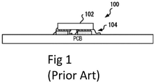
- FIG. 1 shows a section of a system 100 in which a device 102 is shown as being soldered to solder pads on a PCB. As depicted, due to a small size, there is a likelihood that solder material 104 may touch sidewalls of the device 102.
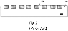
- a known device is shown in Figure 2 .
- a plurality of identical devices may be fabricated simultaneously on a semiconductor wafer 200.
- Each device is shown to have two contact pads 204.
- the device may have different number of contact pads depending on the type of device. If the device is a diode, two contact pads are necessary. However, if the device is a complex circuit having a plurality of components, the number of contact pads in each device may vary.
- An isolation layer 206 is formed over the surface of the semiconductor wafer 200.
- the isolation layer 206 may be made of a polyimide or a similar polymer that offers similar electrical isolation characteristics and strength. In some embodiments, silicon oxide may be used.
- a semiconductor device comprises a pocket, a solderable or glueable re-distribution layer arranged in the pocket, a die comprising at least two contacts, an isolating material for isolating the contacts between each other, wherein all the contacts are fan out to a top surface of the semiconductor device.
- the die can be for example a transistor comprising a base contact, a collector contact and an emitter contact.
- the pocket may comprise sidewalls of about 45 degrees.
- the die is arranged downwards, so that the base contact and the emitter contact are facing the bottom of the semiconductor device, and so that the collector contact is facing the top of the semiconductor device.
- the solderable or glueable re-distribution layer comprises a first re-distribution layer part and a second re-distribution layer part, wherein the first re-distribution layer part and the second re-distribution layer part are isolated from each other by the isolating material.
- the emitter contact is connected to the first re-distribution layer part and the base contact is connected to the second re-distribution layer part. In this way all three contacts, namely the emitter contact via the first re-distribution layer part, the base contact via the second re-distribution layer part, and the collector contact are fan out to the top surface of the semiconductor device.
- the die is arranged upwards, so that the base contact and the emitter contact are facing the top of the semiconductor device, and so that the collector contact is facing the bottom of the semiconductor device.
- the collector contact is connected to the re-distribution layer. In this way, all three contacts, namely the emitter contact, the base contact, and the collector contact via the re-distribution layer, are fan out to the top surface of the semiconductor device.
- the die is arranged on side.
- the solderable or glueable re-distribution layer comprises a first re-distribution layer part and a second re-distribution layer part, wherein the first re-distribution layer part and the second re-distribution layer part are isolated from each other by the isolating material.
- the second re-distribution layer part comprises a third re-distribution layer part and a fourth re-distribution layer part, wherein the third re-distribution layer part and the fourth re-distribution layer part are isolated from each other by the isolating material.
- the collector contact is connected to the first re-distribution layer part
- the emitter contact is connected to the third re-distribution layer part
- the base contact is connected to the fourth re-distribution layer part.
- the invention also relates to an automotive part comprising a semiconductor device as described in the example embodiments above and any similar embodiments.
- the invention also relates to a method of producing a semiconductor device as described in the example embodiments above and any similar embodiments.
- a semiconductor device and a method of producing a semiconductor device as described in the example embodiments above, or any similar embodiments, has all contacts on the same side. Such fan out of the semiconductor device contacts secures the low costs of the semiconductor device production and at the same time eliminates the need for wire bond, lead frames and/or moulding.
- An embodiment of the invention relates to a vertical designed semiconductor device, e.g. a diode, a transistor, etc. having solderable/glueable contacts on both sides of the semiconductor device, wherein the semiconductor device is placed inside a pre-formed carrier.
- the preformed carrier is coated with conductive paths allowing to move all contacts to one side of the package of the semiconductor device.
- the pre-formed carrier is designed with bevelled side walls to allow the application of a solderable/glueable redistribution layer, conductor tracks, on top of the pre-formed carrier surface.
- the paths can be created e.g. using printing, plating or equivalent technologies.
- the semiconductor device which will be placed inside a pre-formed pocket of a fan-out carrier, requires solderable/glueable contacts on both, the top and the bottom surface.
- the semiconductor device can be placed inside a pre-formed pocket and soldered/glued to a redistribution layer.
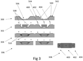
- FIG. 3 An embodiment of the invention is shown in Figure 3 .
- the embodiment is presented for a transistor 308 comprising a base 400, a collector 402 and an emitter 404.
- the embodiment is not limited to this transistor example, it is applicable to any semiconductor device.
- pockets 506 with a sidewall of about 45 degrees or any other suitable angle are created.
- the pockets 506 are partially coated with a solderable/glueable re-distribution layer 500. This can be achieved by printing, plating, or any other equivalent technology.
- the solderable/glueable re-distribution layer 500 comprises a first re-distribution layer part 502 and a second re-distribution layer part 504.
- a die comprising a base contact and an emitter contact
- a die is placed with its face downwards, i.e. flipped, in the pocket.
- the base contact 400 and the emitter contact 404 are connected to the second re-distribution layer part 504 and the second re-distribution layer part 502 respectively.
- connection between the base contact 400 and the emitter contact 404 and the second re-distribution layer part 504 and the first re-distribution layer part 502 can be done glue, soldering, or any other suitable way.
- the gaps 508 between the dies and the pockets are filled with an isolating material 510.
- an isolating material secures the stability of the dies and protects the dies against environment.
- a separation of the transistors is executed.
- a top view of a separated transistor is indicated with the reference number 308.
- a semiconductor device in this particular example a transistor, has all contacts on the same side. Such fan out of the transistor contacts secures the low costs of the semiconductor device production and at the same time eliminates the need for wire bond, lead frames and/or moulding.
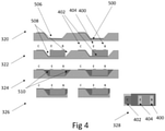
- FIG. 4 An embodiment of the invention is shown in Figure 4 .
- the embodiment is presented for a transistor 328 comprising a base 400, a collector 402 and an emitter 404.
- the embodiment is not limited to this transistor example, it is applicable to any semiconductor device.
- pockets 506 with a sidewall of about 45 degrees or any other suitable angle are created.
- the pockets 506 are partially coated with a solderable/glueable re-distribution layer 500. This can be achieved by printing, plating, or any other equivalent technology.
- a die comprising a base contact 400 and an emitter contact 404, is placed with its face upwards, in the pocket 506.
- the collector contact 402 is placed with its face downwards. In this way the collector contact 402 is connected to the solderable/glueable re-distribution layer 500.
- connection between the collector contact 402 and the solderable/glueable re-distribution layer 500 can be done glue, soldering, or any other suitable way.
- the gaps 508 between the dies and the pockets are filled with an isolating material 510.
- an isolating material secures the stability of the dies and protects the dies against environment.
- a separation of the transistors is executed.
- a top view of a separated transistor is indicated with the reference number 328.
- the transistor 328 shown in Figure 4 has all contacts on the same side. Such fan out of the transistor contacts secures the low costs of the semiconductor device production and at the same time eliminates the need for wire bond, lead frames and/or moulding.
- the package of this semiconductor device does not require vias since the form of the carrier allows to have only one redistribution layer on one side of the carrier.
- FIG. 5 An embodiment of the invention is shown in Figure 5 .
- the embodiment is presented for a transistor 348 comprising a base 400, a collector 402 and an emitter 404.
- the embodiment is not limited to this transistor example, it is applicable to any semiconductor device.
- pockets 506 with a sidewall of about 45 degrees or any other suitable angle are created.
- the pockets 506 are partially coated with a solderable/glueable re-distribution layer 500.
- the solderable/glueable re-distribution layer 500 comprises a first re-distribution layer part 502 and a second re-distribution layer part 504.
- the second re-distribution layer part 504 comprises two parts, a third re-distribution layer part 520 and a fourth re-distribution layer part which are isolated from each other.
- the third re-distribution layer part 520 is visible in Figure 5
- the fourth re-distribution layer part is behind the third re-distribution layer part and it is therefore not visible in Figure 5 .
- a die comprising a base contact 400, the collector contact 402 and an emitter contact 404, is placed on side in the pocket.
- the side walls of the die are insulated.
- the collector contact 402 is connected to the first re-distribution layer part 502.
- the emitter contact 404 and the base contact 400 are connected to the third re-distribution layer part 520 and the fourth re-distribution layer part, respectively.
- connection between the collector contact 402, the base contact 400 and the emitter contact 404 with the first re-distribution layer part 502, the third re-distribution layer part 520 and the fourth re-distribution layer part, respectively, can be done glue, soldering, or any other suitable way.
- the gaps 508 between the dies and the pockets are filled with an isolating material 510.
- an isolating material secures the stability of the dies and protects the dies against environment.
- a separation of the transistors is executed.
- a top view of a separated transistor is indicated with the reference number 348.
- the transistor 348 shown in Figure 5 has all contacts on the same side. Such fan out of the transistor contacts secures the low costs of the semiconductor device production and at the same time eliminates the need for wire bond, lead frames and/or moulding.
- the package of this semiconductor device does not require vias since the form of the carrier allows to have only one redistribution layer on one side of the carrier.
Landscapes
- Die Bonding (AREA)
- Structures Or Materials For Encapsulating Or Coating Semiconductor Devices Or Solid State Devices (AREA)
Priority Applications (3)
| Application Number | Priority Date | Filing Date | Title |
|---|---|---|---|
| EP20186729.8A EP3944304A1 (fr) | 2020-07-20 | 2020-07-20 | Dispositif semi-conducteur et son procédé de fabrication |
| CN202110813737.5A CN113964099A (zh) | 2020-07-20 | 2021-07-19 | 半导体装置及其制造方法 |
| US17/380,220 US20220020679A1 (en) | 2020-07-20 | 2021-07-20 | Semiconductor device and a method of manufacture |
Applications Claiming Priority (1)
| Application Number | Priority Date | Filing Date | Title |
|---|---|---|---|
| EP20186729.8A EP3944304A1 (fr) | 2020-07-20 | 2020-07-20 | Dispositif semi-conducteur et son procédé de fabrication |
Publications (1)
| Publication Number | Publication Date |
|---|---|
| EP3944304A1 true EP3944304A1 (fr) | 2022-01-26 |
Family
ID=71737994
Family Applications (1)
| Application Number | Title | Priority Date | Filing Date |
|---|---|---|---|
| EP20186729.8A Pending EP3944304A1 (fr) | 2020-07-20 | 2020-07-20 | Dispositif semi-conducteur et son procédé de fabrication |
Country Status (3)
| Country | Link |
|---|---|
| US (1) | US20220020679A1 (fr) |
| EP (1) | EP3944304A1 (fr) |
| CN (1) | CN113964099A (fr) |
Citations (6)
| Publication number | Priority date | Publication date | Assignee | Title |
|---|---|---|---|---|
| US6340842B1 (en) * | 1998-04-02 | 2002-01-22 | Oki Electric Industry Co., Ltd. | Semiconductor device in a recess of a semiconductor plate |
| US20020008325A1 (en) * | 2000-05-11 | 2002-01-24 | Mitutoyo Corporation | Functional device unit and method of producing the same |
| US6867499B1 (en) * | 1999-09-30 | 2005-03-15 | Skyworks Solutions, Inc. | Semiconductor packaging |
| US9305852B1 (en) * | 2014-11-11 | 2016-04-05 | Texas Instruments Incorporated | Silicon package for embedded electronic system having stacked semiconductor chips |
| US20170301596A1 (en) * | 2014-11-06 | 2017-10-19 | Texas Instruments Incorporated | Silicon package for embedded semiconductor chip and power converter |
| US20180005993A1 (en) * | 2016-06-30 | 2018-01-04 | Winbond Electronics Corp. | Package and packaging process of a semiconductor device |
Family Cites Families (22)
| Publication number | Priority date | Publication date | Assignee | Title |
|---|---|---|---|---|
| TWI227570B (en) * | 2003-12-11 | 2005-02-01 | South Epitaxy Corp | Light-emitting diode packaging structure |
| KR101181112B1 (ko) * | 2005-10-27 | 2012-09-14 | 엘지이노텍 주식회사 | 발광 다이오드, 발광 다이오드 제조 방법 및 발광 다이오드 모듈 |
| US20070210340A1 (en) * | 2006-03-10 | 2007-09-13 | Zampardi Peter J | GaAs power transistor |
| US8201326B2 (en) * | 2008-12-23 | 2012-06-19 | Infineon Technologies Ag | Method of manufacturing a semiconductor device |
| US8513062B2 (en) * | 2010-02-16 | 2013-08-20 | Infineon Technologies Ag | Method of manufacturing a semiconductor device with a carrier having a cavity and semiconductor device |
| TWI462340B (zh) * | 2010-09-08 | 2014-11-21 | 晶元光電股份有限公司 | 一種發光結構及其製造方法 |
| WO2012049742A1 (fr) * | 2010-10-13 | 2012-04-19 | 日立オートモティブシステムズ株式会社 | Capteur d'écoulement et son procédé de production, et module de capteur d'écoulement et son procédé de production |
| US8994048B2 (en) * | 2010-12-09 | 2015-03-31 | Stats Chippac, Ltd. | Semiconductor device and method of forming recesses in substrate for same size or different sized die with vertical integration |
| US9178123B2 (en) * | 2012-12-10 | 2015-11-03 | LuxVue Technology Corporation | Light emitting device reflective bank structure |
| US9159700B2 (en) * | 2012-12-10 | 2015-10-13 | LuxVue Technology Corporation | Active matrix emissive micro LED display |
| US9252375B2 (en) * | 2013-03-15 | 2016-02-02 | LuxVue Technology Corporation | Method of fabricating a light emitting diode display with integrated defect detection test |
| US20140306331A1 (en) * | 2013-04-11 | 2014-10-16 | Infineon Technologies Austria Ag | Chip and chip arrangement |
| US9484504B2 (en) * | 2013-05-14 | 2016-11-01 | Apple Inc. | Micro LED with wavelength conversion layer |
| US9111464B2 (en) * | 2013-06-18 | 2015-08-18 | LuxVue Technology Corporation | LED display with wavelength conversion layer |
| US9640519B2 (en) * | 2014-11-11 | 2017-05-02 | Texas Instruments Incorporated | Photo-sensitive silicon package embedding self-powered electronic system |
| JP6676308B2 (ja) * | 2015-08-07 | 2020-04-08 | ローム株式会社 | 半導体装置 |
| JP2017037900A (ja) * | 2015-08-07 | 2017-02-16 | ローム株式会社 | 半導体装置およびその製造方法 |
| JP6595840B2 (ja) * | 2015-08-20 | 2019-10-23 | ローム株式会社 | 半導体装置およびその製造方法 |
| KR102503215B1 (ko) * | 2016-03-28 | 2023-02-24 | 삼성전자 주식회사 | 발광 소자 패키지 |
| JP6789886B2 (ja) * | 2017-06-09 | 2020-11-25 | 株式会社東芝 | 電子装置 |
| US11264527B2 (en) * | 2018-10-01 | 2022-03-01 | Medtronic, Inc. | Integrated circuit package and system using same |
| JP7267767B2 (ja) * | 2019-02-20 | 2023-05-02 | ローム株式会社 | 半導体装置および半導体装置の製造方法 |
-
2020
- 2020-07-20 EP EP20186729.8A patent/EP3944304A1/fr active Pending
-
2021
- 2021-07-19 CN CN202110813737.5A patent/CN113964099A/zh active Pending
- 2021-07-20 US US17/380,220 patent/US20220020679A1/en active Pending
Patent Citations (6)
| Publication number | Priority date | Publication date | Assignee | Title |
|---|---|---|---|---|
| US6340842B1 (en) * | 1998-04-02 | 2002-01-22 | Oki Electric Industry Co., Ltd. | Semiconductor device in a recess of a semiconductor plate |
| US6867499B1 (en) * | 1999-09-30 | 2005-03-15 | Skyworks Solutions, Inc. | Semiconductor packaging |
| US20020008325A1 (en) * | 2000-05-11 | 2002-01-24 | Mitutoyo Corporation | Functional device unit and method of producing the same |
| US20170301596A1 (en) * | 2014-11-06 | 2017-10-19 | Texas Instruments Incorporated | Silicon package for embedded semiconductor chip and power converter |
| US9305852B1 (en) * | 2014-11-11 | 2016-04-05 | Texas Instruments Incorporated | Silicon package for embedded electronic system having stacked semiconductor chips |
| US20180005993A1 (en) * | 2016-06-30 | 2018-01-04 | Winbond Electronics Corp. | Package and packaging process of a semiconductor device |
Also Published As
| Publication number | Publication date |
|---|---|
| CN113964099A (zh) | 2022-01-21 |
| US20220020679A1 (en) | 2022-01-20 |
Similar Documents
| Publication | Publication Date | Title |
|---|---|---|
| US6828665B2 (en) | Module device of stacked semiconductor packages and method for fabricating the same | |
| US5247423A (en) | Stacking three dimensional leadless multi-chip module and method for making the same | |
| US10681801B2 (en) | Mounting assembly with a heatsink | |
| US9130064B2 (en) | Method for fabricating leadframe-based semiconductor package with connecting pads top and bottom surfaces of carrier | |
| KR20000048471A (ko) | 다수의 전원/접지면을 갖는 볼 그리드 어레이 패키지 | |
| US20090261465A1 (en) | Semiconductor device and its manufacturing method | |
| US20090310322A1 (en) | Semiconductor Package | |
| US7790504B2 (en) | Integrated circuit package system | |
| US20070130554A1 (en) | Integrated Circuit With Dual Electrical Attachment Pad Configuration | |
| KR101474189B1 (ko) | 집적회로 패키지 | |
| US6573595B1 (en) | Ball grid array semiconductor package with resin coated metal core | |
| JP2001168233A (ja) | 多重回線グリッド・アレイ・パッケージ | |
| IE50430B1 (en) | Integrated circuit package | |
| US7498666B2 (en) | Stacked integrated circuit | |
| EP3944304A1 (fr) | Dispositif semi-conducteur et son procédé de fabrication | |
| US20050023659A1 (en) | Semiconductor chip package and stacked module having a functional part and packaging part arranged on a common plane | |
| KR20010063236A (ko) | 적층 패키지와 그 제조 방법 | |
| US10236270B2 (en) | Interposer and semiconductor module for use in automotive applications | |
| KR100199286B1 (ko) | 홈이 형성된 인쇄 회로 기판을 갖는 칩 스케일 패키지 | |
| US20030080418A1 (en) | Semiconductor device having power supply pads arranged between signal pads and substrate edge | |
| JPS617657A (ja) | マルチチツプパツケ−ジ | |
| KR100762871B1 (ko) | 칩크기 패키지 제조방법 | |
| KR20020028473A (ko) | 적층 패키지 | |
| KR19980025890A (ko) | 리드 프레임을 이용한 멀티 칩 패키지 | |
| KR20030012192A (ko) | 다이 적층형 윈도우 칩 스케일 패키지 |
Legal Events
| Date | Code | Title | Description |
|---|---|---|---|
| PUAI | Public reference made under article 153(3) epc to a published international application that has entered the european phase |
Free format text: ORIGINAL CODE: 0009012 |
|
| STAA | Information on the status of an ep patent application or granted ep patent |
Free format text: STATUS: THE APPLICATION HAS BEEN PUBLISHED |
|
| AK | Designated contracting states |
Kind code of ref document: A1 Designated state(s): AL AT BE BG CH CY CZ DE DK EE ES FI FR GB GR HR HU IE IS IT LI LT LU LV MC MK MT NL NO PL PT RO RS SE SI SK SM TR |
|
| STAA | Information on the status of an ep patent application or granted ep patent |
Free format text: STATUS: REQUEST FOR EXAMINATION WAS MADE |
|
| 17P | Request for examination filed |
Effective date: 20220726 |
|
| RBV | Designated contracting states (corrected) |
Designated state(s): AL AT BE BG CH CY CZ DE DK EE ES FI FR GB GR HR HU IE IS IT LI LT LU LV MC MK MT NL NO PL PT RO RS SE SI SK SM TR |
|
| STAA | Information on the status of an ep patent application or granted ep patent |
Free format text: STATUS: EXAMINATION IS IN PROGRESS |