EP3945424B1 - Procédé de gestion d'alimentation de mémoire et système de processeur - Google Patents
Procédé de gestion d'alimentation de mémoire et système de processeur Download PDFInfo
- Publication number
- EP3945424B1 EP3945424B1 EP21175301.7A EP21175301A EP3945424B1 EP 3945424 B1 EP3945424 B1 EP 3945424B1 EP 21175301 A EP21175301 A EP 21175301A EP 3945424 B1 EP3945424 B1 EP 3945424B1
- Authority
- EP
- European Patent Office
- Prior art keywords
- memory bank
- memory
- heap
- bank
- section identifier
- Prior art date
- Legal status (The legal status is an assumption and is not a legal conclusion. Google has not performed a legal analysis and makes no representation as to the accuracy of the status listed.)
- Active
Links
Images




Classifications
-
- G—PHYSICS
- G06—COMPUTING OR CALCULATING; COUNTING
- G06F—ELECTRIC DIGITAL DATA PROCESSING
- G06F1/00—Details not covered by groups G06F3/00 - G06F13/00 and G06F21/00
- G06F1/26—Power supply means, e.g. regulation thereof
- G06F1/32—Means for saving power
- G06F1/3203—Power management, i.e. event-based initiation of a power-saving mode
- G06F1/3234—Power saving characterised by the action undertaken
- G06F1/325—Power saving in peripheral device
- G06F1/3275—Power saving in memory, e.g. RAM, cache
-
- G—PHYSICS
- G06—COMPUTING OR CALCULATING; COUNTING
- G06F—ELECTRIC DIGITAL DATA PROCESSING
- G06F12/00—Accessing, addressing or allocating within memory systems or architectures
- G06F12/02—Addressing or allocation; Relocation
- G06F12/0223—User address space allocation, e.g. contiguous or non contiguous base addressing
- G06F12/023—Free address space management
-
- G—PHYSICS
- G06—COMPUTING OR CALCULATING; COUNTING
- G06F—ELECTRIC DIGITAL DATA PROCESSING
- G06F1/00—Details not covered by groups G06F3/00 - G06F13/00 and G06F21/00
- G06F1/26—Power supply means, e.g. regulation thereof
- G06F1/32—Means for saving power
- G06F1/3203—Power management, i.e. event-based initiation of a power-saving mode
- G06F1/3234—Power saving characterised by the action undertaken
- G06F1/3287—Power saving characterised by the action undertaken by switching off individual functional units in the computer system
-
- G—PHYSICS
- G06—COMPUTING OR CALCULATING; COUNTING
- G06F—ELECTRIC DIGITAL DATA PROCESSING
- G06F12/00—Accessing, addressing or allocating within memory systems or architectures
- G06F12/02—Addressing or allocation; Relocation
- G06F12/06—Addressing a physical block of locations, e.g. base addressing, module addressing, memory dedication
-
- G—PHYSICS
- G06—COMPUTING OR CALCULATING; COUNTING
- G06F—ELECTRIC DIGITAL DATA PROCESSING
- G06F8/00—Arrangements for software engineering
- G06F8/70—Software maintenance or management
- G06F8/75—Structural analysis for program understanding
-
- H—ELECTRICITY
- H04—ELECTRIC COMMUNICATION TECHNIQUE
- H04L—TRANSMISSION OF DIGITAL INFORMATION, e.g. TELEGRAPHIC COMMUNICATION
- H04L63/00—Network architectures or network communication protocols for network security
- H04L63/04—Network architectures or network communication protocols for network security for providing a confidential data exchange among entities communicating through data packet networks
- H04L63/0428—Network architectures or network communication protocols for network security for providing a confidential data exchange among entities communicating through data packet networks wherein the data content is protected, e.g. by encrypting or encapsulating the payload
- H04L63/0442—Network architectures or network communication protocols for network security for providing a confidential data exchange among entities communicating through data packet networks wherein the data content is protected, e.g. by encrypting or encapsulating the payload wherein the sending and receiving network entities apply asymmetric encryption, i.e. different keys for encryption and decryption
-
- H—ELECTRICITY
- H04—ELECTRIC COMMUNICATION TECHNIQUE
- H04L—TRANSMISSION OF DIGITAL INFORMATION, e.g. TELEGRAPHIC COMMUNICATION
- H04L63/00—Network architectures or network communication protocols for network security
- H04L63/16—Implementing security features at a particular protocol layer
- H04L63/166—Implementing security features at a particular protocol layer at the transport layer
-
- G—PHYSICS
- G06—COMPUTING OR CALCULATING; COUNTING
- G06F—ELECTRIC DIGITAL DATA PROCESSING
- G06F2212/00—Indexing scheme relating to accessing, addressing or allocation within memory systems or architectures
- G06F2212/10—Providing a specific technical effect
- G06F2212/1028—Power efficiency
-
- Y—GENERAL TAGGING OF NEW TECHNOLOGICAL DEVELOPMENTS; GENERAL TAGGING OF CROSS-SECTIONAL TECHNOLOGIES SPANNING OVER SEVERAL SECTIONS OF THE IPC; TECHNICAL SUBJECTS COVERED BY FORMER USPC CROSS-REFERENCE ART COLLECTIONS [XRACs] AND DIGESTS
- Y02—TECHNOLOGIES OR APPLICATIONS FOR MITIGATION OR ADAPTATION AGAINST CLIMATE CHANGE
- Y02D—CLIMATE CHANGE MITIGATION TECHNOLOGIES IN INFORMATION AND COMMUNICATION TECHNOLOGIES [ICT], I.E. INFORMATION AND COMMUNICATION TECHNOLOGIES AIMING AT THE REDUCTION OF THEIR OWN ENERGY USE
- Y02D10/00—Energy efficient computing, e.g. low power processors, power management or thermal management
Definitions
- This disclosure relates to a method for memory power management and processor system including power management.
- Low power processor systems such as microcontrollers may be configured to operate as Internet of Things (IoT) devices which may have a relatively long inactive period and a shorter active period of operation.
- IoT Internet of Things
- the IoT system including the microcontroller may be in a sleep mode to minimize the power consumption.
- the device may then transition from the sleep mode to an active mode to execute the required operations before transitioning back to a sleep mode.
- devices which operate as end-points in a network such as a Zigbee or other network may operate as a so-called sleepy device.
- Such a device when included in a network may also have to execute one or more cryptographic operations when in active mode for example to authenticate the device within the network or to authenticate a particular data transfer.
- US 2018/253556 A1 describes the selective restoration and authentication of a secure image.
- a method of power management for a processor system including a processor coupled to a memory, wherein the comprises a plurality of memory banks, the memory further comprising a region configurable as a heap region, wherein the processor is operable to execute instructions comprising one or more cryptographic operations; and wherein the method comprises: allocating at least one memory bank to the heap region dependent on a predetermined memory size required for execution of at least one cryptographic operation; allocating at least one further memory bank to the heap region; and switching from a first operating mode to a second operating mode by setting the at least one memory bank to an active state; setting the at least one further memory bank to an active state; switching from the second operating mode to the first operating mode by: setting the at least one memory bank to a retention state, wherein a memory bank in a retention state cannot be read but data in the memory bank are retained ; setting the at least one further memory bank to a power-down state.
- the at least one memory bank may be configured to store a public key.
- the at least one cryptographic operation may comprise a transport layer security (TLS) handshake operation.
- TLS transport layer security
- the at least one cryptographic operation may comprise at least one of an encryption operation and a decryption operation.
- the at least one memory bank and the at least one further memory bank may be non-contiguous.
- allocating at least one memory bank to the heap region may further comprise dividing the heap region into a plurality of sections, each section corresponding to a respective memory bank.
- the method may further comprise providing an identifier for each cryptographic operation, providing the required heap size for each cryptographic operation and providing a section identifier comprising the address of a memory bank used as a starting point for each cryptographic operation.
- the method may further comprise switching from the first operating mode to the second operating mode by: setting a first memory bank to the active state; checking whether the section identifier corresponds to the first memory bank; in response to the section identifier corresponding to the first memory bank, determining whether the heap size exceeds the available memory in the first memory bank; in response to the heap size exceeding the available memory in the first memory bank; setting a second memory bank to the active state; in response to the section identifier not corresponding to the first memory bank, setting a third memory bank corresponding to the section identifier to the active state.
- the method may further comprise checking whether the section identifier corresponds to the first memory bank; allocating the first memory bank to the heap region; in response to the section identifier corresponding to the first memory bank, determining whether the heap size exceeds the available memory in the first memory bank; in response to the heap size exceeding the available memory in the first memory bank; allocating a second memory bank to the heap region; in response to the section identifier not corresponding to the first memory bank, allocating a third memory bank corresponding to the section identifier to the heap region.
- the method may further comprise determining the predetermined memory size required for execution of at least one cryptographic operation by : determining the memory size to store the crypto-session elements for the at least one cryptographic operation; determining the memory size to store the at least one cryptographic operation.
- determining the predetermined memory size required for execution of at least one cryptographic operation may further comprise running a static code analysis and a run-time code analysis.
- a processor system comprising a processor coupled to a memory comprising a plurality of memory banks, the memory further comprising a region configurable as a heap region, wherein the processor is operable to execute instructions comprising one or more cryptographic operations; and wherein the processor system is configured to: allocate at least one memory bank to the heap region dependent on a predetermined memory size required for execution of at least one cryptographic operation; allocate at least one further memory bank to the heap region; further configured to switch from a first operating mode to a second operating mode by: setting the at least one memory bank to an active state; setting the at least one further memory bank to an active state; and further configured to switch from the second operating mode to the first operating mode by setting the at least one memory bank to a retention state wherein a memory bank in a retention state cannot be read but data in the memory bank are retained and setting the at least one further memory bank to a power-down state.
- the processor system may be further configured to provide an identifier for each cryptographic operation, provide the required heap size for each cryptographic operation and provide a section identifier comprising the address of a memory bank used as a starting point for each cryptographic operation.
- the processor system may be further configured switch between a first operating mode and a second operating mode by setting a first memory bank to the active state; checking whether the section identifier corresponds to the first memory bank; in response to the section identifier corresponding to the first memory bank, determining whether the heap size exceeds the available memory in the first memory bank ; in response to the heap size exceeding the available memory in the first memory bank ; setting a second memory bank to the active state; in response to the section identifier not corresponding to the first memory bank, setting a third memory bank corresponding to the section identifier to the active state.
- the processor system may be further configured to check whether the section identifier corresponds to the first memory bank; allocate the first memory bank to the heap region; in response to the section identifier corresponding to the first memory bank, determining whether the heap size exceeds the available memory in the first memory bank; in response to the heap size exceeding the available memory in the first memory bank ; allocating a second memory bank to the heap region; in response to the section identifier not corresponding to the first memory bank, allocating a third memory bank corresponding to the section identifier to the heap region.
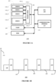
- FIG. 1A shows an example processor system 100.
- the processor system 100 may be a single device including a central processing unit (CPU) 108 which may be a microprocessor or microcontroller.
- the CPU 108 may include a number of registers including a stack pointer register.
- the processor system 100 may further include a communication interface 112 which may be for example a wired or wireless transceiver for communication with other devices, a static random access memory (SRAM) 110, a read only memory (ROM) 104 and a non-volatile Flash memory 102.
- the Flash 102 and ROM 104 may store the software or firmware executable by the CPU 108.
- the SRAM 110 may include a number of memory banks 110_1, 110_2, 110_3, 110_4 of different sizes coupled to an SRAM controller 106 by connections 116_1, 116_2, 116_3, 116_4.
- processor system 100 four memory banks are shown but in other examples fewer or more memory banks may be used. In other example systems more than one SRAM controller 106 may be used to control further memory banks.
- the CPU 102, communication interface 112, SRAM controller 106, ROM 104 and Flash 102 may be coupled together via a communication bus 114.
- the processor system 100 may be implemented on a single device for example a system-on-chip (SoC).
- SoC system-on-chip
- one or more of the Flash 102, ROM 104 and the SRAM 110 may be implemented on a separate device or separate devices.
- the SRAM controller 106 may control the memory banks 110_1, 110_2, 110_3, 110_4 and provide data access to the communication bus 114.
- the SRAM controller 106 may control the power to each memory bank 110_1, 110_2, 110_3, 110_4 independently according to the following operating states.
- the processor system 100 may also include other peripherals (not shown) which may be coupled to the communication bus 114.
- the SRAM controller 106 and other peripherals may have interrupt connections (not shown ) to the CPU 102.
- SRAM as used in the present disclosure may refer to a volatile read-write memory which loses information when power is removed.
- non-volatile memory may refer to any read-write memory which retains information when power is removed, for example Flash memory.
- Memory addresses as referred to in the present disclosure may refer to physical addresses or virtual addresses.
- Figure 1B illustrates a plot 150 of the power consumption on the y-axis 154 versus time on the x-axis 152 in different operating modes for the processor system 100 configured as an IoT device.
- the IOT device may execute a full start-up following which the IOT device may be in a phase of normal operation 158 which may be referred to as a wake cycle or wake up cycle.
- Phases 156 and 158 may consume relatively large amounts of power.
- the IOT device may execute a power-down operation to switch to a lower power mode which may be a standby or sleep mode during an inactive time period 160 which may be a much longer period compared to the active period 158.
- the IOT device may then repeatedly switch or transition between a normal operating mode during the active phase 158 and the lower-power mode during the inactive phase 160.
- FIG. 2 shows an example memory map 200 for a processor system having an SRAM controller and eight memory banks.
- the main memory map 214 consists of a flash region 202, a rom region 204, an SRAM control region 206 and a further region 208.
- the main memory map 210 also has reserved memory regions. The size of the SRAM control region corresponds to the total memory of each of the memory modules 210_1 to 210_8.
- Figure 3 shows an example linker placement 250 for an application that shows a typical algorithm using the different states of the memory banks of figure 2 .
- This example is based on the OpenThread stack which is a mesh networking stack for low-power devices over IPv6.
- a MTD (Minimal Thread Device) application built with the Mbed Transport Layer Security (TLS) library implements the TLS and Secure sockets layer (SLL) protocols together with the respective cryptographic algorithms.
- Table 1 shows the following sections of classical layout for a C program for an ARM-based processor system for the example application: Table 1 Text Data Bss Total (Dec) Total (Hex) 249832 612 26364 276808 43948
- Two banks of 16Kb 210_1, 210_2 are used mainly for a reserved section 254, Thread and Application Data 256 section, bss section 258, and Heap 260 while one 4Kb bank 210_8 is used for the Stack 262.
- these 3 memory banks 210_1, 210_2 and 210_8 are kept in retention state for saving power.
- the Power manager controls the memory controller to shut down the memory banks 210_3, 210_4, 210_5, 210_6, 210_7.
- the Bss section includes approximately 26Kb. Part of this section is 12Kb of the heap space needed for cryptographic operations.
- the memory for the heap region is partly using predefined blocks of memory in the application code which are reserved during compile-time rather than blocks which are dynamically allocated and freed during run-time, for example using the C programming language malloc() and free() function calls.
- the heap is at least partly indicated as being part of the Bss section but it will be appreciated that the heap region may be considered to be a separate region in memory.
- the Heap space starts in the first 16Kb bank 210_1 and ends in the second 16Kb bank 210_2.
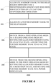
- Figure 4 shows a method of memory power management 300 according to an embodiment.
- the method 300 may be applied to a processor system, for example the processor system 100 having multiple memory banks of SRAM.
- a memory bank may be allocated to the heap region dependent on a predetermined memory size required for the execution of at least one cryptographic operation.
- a further memory bank may be allocated to the heap region.
- the allocated memory bank may be set to an active state and the further memory bank may also be set to an active state.
- the allocated memory bank may be set to a retention state and the further memory bank may be set to an inactive or power-down state.
- the first operating mode may include operating modes such as sleep mode or standby mode or where a device is powered off.
- the term operating mode as used in the present disclosure may include modes in which a device implementing the method is inactive as well as active.
- the method 300 uses precomputed required space for each crypto operation such that the heap space can be split in multiple regions by taking into consideration the size of the SRAM banks. Using this method, the smallest memory bank is put in the active state only when a crypto computation is imminent. This precomputed required space for each crypto operation might be determined by a combination of static and runtime code analysis.
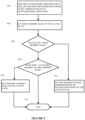
- Figure 5 shows a method of memory power management 400 according to an embodiment.
- the method 400 may be applied to a processor system, for example the processor system 100 having multiple memory banks of SRAM.
- the method 400 may be applied during a wake up cycle which may be a first part of the active cycle during or after transitioning from a standby mode or low power mode for a low-power microcontrollers system.
- step 402 for each cryptographic operation an identifier, the required heap size, section identifier including start address may be provided.
- a first memory bank which may be denoted as Bank common may be set to an active state from a retention state.
- step 406 a check may be made to determine whether the section identifier corresponds to the first memory bank Bank common .
- the first memory bank Bank common may also be referred to as the crypto-session memory bank. Part of Bank common is used to store crypto-session information.
- the section identifier corresponding to Bank common may be denoted as Scommon.
- step 408 a comparison is made between the predetermined heap size and the available memory in the first memory bank. If the predetermined heap size is greater than available memory, the method proceeds to step 410 and a second memory bank may transition to an active state from a down state. Following step 410 the method 400 terminates at step 414.
- step 408 if the heap size is less than or equal to the available memory in the first memory bank, the method proceeds straight to step 414 where the process terminates.
- step 406 if the section identifier does not correspond to the first memory bank, the method proceeds to step 412 and a memory bank corresponds to the address indicated by the section identifier transitions to an active state from a power down state. Successive memory banks after the first memory bank identified by the section identifier may also be used depending on the predetermined heap size provided in step 402. These memory banks may transition to the active state from a power-down state. Following step 412, the method 400 proceeds to step 414 and terminates.
- Method 400 may be implemented for example in software executable on a central processor included as part of a processor system which implements the power management method 400 before each crypto operation.
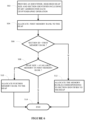
- Figure 6 shows a method of memory heap allocation 500 according to an embodiment.
- the method 500 may be applied to a processor system, for example the processor system 100 having multiple memory banks of SRAM.
- the memory heap allocation method 500 is complementary to the power management method 400.
- the method 500 may be applied during a wake up cycle for a low-power microcontrollers system.
- step 502 for each cryptographic operation implemented by the processor system an identifier, the required heap size and a section identifier including a start address may be provided.
- a first memory bank Bank common may be allocated to the heap.
- the first memory bank may also be referred to as the crypto-session memory bank
- a check may be made to determine whether the section identifier corresponds to the first memory bank Bank common which may be in a retention state.
- the section identifier corresponding to Bank common may be denoted as S common . If the section identifier is equal to S common , the method proceeds to step 508 where a comparison is made between the predetermined heap size and the first memory bank size.
- step 510 a second memory bank may be allocated to the heap. Bank common already stores the crypto-session information so some space is not available for the heap. Following step 510 the method 500 terminates at step 514.
- step 508 if the heap size is less than or equal to the first memory bank size, the method proceeds straight to step 514 where the process terminates. In some examples in addition to the second memory bank, further memory banks may be allocated.
- step 506 if the section identifier does not correspond to the first memory bank, the method proceeds to step 512 and a memory bank corresponding to the memory bank having an address indicated by the section identifier is allocated to the heap. Successive memory banks after the first memory bank identified by the section identifier may also be allocated to the heap depending on the predetermined heap size provided in step 502. Following step 512, the method 500 proceeds to step 514 and terminates.
- Method 500 may be implemented for example in software executable on a processor which implements the heap allocation method 500 before each crypto operation.
- Figure 7 shows a method 600 of determining a crypto operation identifier according to an embodiment.
- step 602 the main sections of the application that use crypto operations and allocates heap space are identified. This identification step may be done for example by static code analysis.
- the delimiter for these sections may be a power-down cycle in which a device may transition to a lower power operating mode such as a sleep or standby mode.
- An identifier may be assigned for each crypto operation denoted as crypto_op_id.
- step 604 the structures that are kept for the duration of the whole crypto session may be identified.
- the following notation is used for these structures: C1, C2..., Cn.
- An identifier (id) may be assigned for each of these structures (struct_id).
- the public key of a peer obtained after a DTLS handshake might be a crypto-session element. This public key may be used for multiple encrypt operations.
- step 606 using run-time analysis, the maximum heap space required by each of these crypto operations and data structures may be determined.
- the DTLS handshake operation could require 8Kb of SRAM, while a decrypt operation could require only 3Kb of SRAM.
- a linker file may be built.
- the most advantageous power-save solution from a SRAM perspective that can accommodate C total Kb may be computed by choosing a continuous SRAM bank subset which can accommodate the C total Kb and which minimize the amount of unused SRAM space.
- a single 4Kb SRAM bank may be chosen.
- a 4Kb and a 8Kb SRAM module may be chosen instead of a 16Kb SRAM module. Two modules, one of 4Kb and one of 8Kb, typically require less power than a 16Kb module.
- the SRAM banks chosen may be contiguous or non-contiguous.
- step 612 a linker section having as starting point address the first SRAM bank chosen before is defined. This section is denoted S common as previously described.
- a global table (notation: Op_table) may be built with entries of the following type:
- This global table may be used for example by power management method 400 and heap allocation method 500.
- Figure 8 shows a linker placement 700 according to an example embodiment. Linker placement as illustrated is for the same application used for linker placement 250 using the memory banks of figure 2 .
- One bank of 16Kb 210_1 is used for a reserve section 702, the Thread and Application Data 704, and the bss section 706.
- the stack 708 is allocated to 4K memory bank 210_8.
- the heap section 710 is allocated in two sections. A first heap section 710_1 is allocated to a 4 K memory bank 210_7 and a second heap section 710_2 is allocated to an 8K section 210_6.
- two SRAM banks 210_7, 210_6, one of 4Kb and one of 8Kb are used and no space is wasted.
- the 4Kb bank 210_7 is kept in retention mode (for keeping the crypto-session structures) while the 8Kb bank 210_6 is totally shut down. So instead of keeping one 16Kb SRAM bank in retention most of the time, only a 4Kb SRAM bank is kept in retention;
- Embodiments describe a method and apparatus for partitioning the heap space by maximizing the hardware capabilities of SRAM modules.
- Embodiments may selectively activate memory banks only when needed and it can dynamically adapt the number of used banks such that this number is kept at a minimum.
- Embodiments described herein are directed to power management for SRAM memories. However, it will be appreciated that the method may be applied to other volatile memory types such as DRAM. with a low power retention mode where only refresh is performed and bus access is disabled The required space for each crypto operations may be precomputed such that the heap space can be split in multiple regions by taking into consideration the size of the SRAM banks. Using methods described herein, the smallest memory bank may be set in the active state only when a crypto computation is imminent.
- a linker file may define more than one section for the heap by taking into consideration the SRAM architecture.
- a heap-allocation method may allocate the crypto-session information in the smallest possible SRAM region. In some examples this region may not be the smallest SRAM bank.
- a power management method may determine during wake cycles which SRAM bank or banks corresponding to the heap should be transitioned to an active state and during sleep cycles determine which SRAM bank corresponding to the heap should be transitioned either to a retention state or power down state.
- processor systems may be configured as IoT devices.
- processor systems may be configured to use OpenThread and or Zigbee software stacks.
- the processor system may be configured to operate as network node clients requiring high level of security and which have relatively long inactive periods.
- the processor system includes a processor coupled to a memory comprising a plurality of memory banks.
- the memory has a region configurable as a heap region.
- the processor system is operable to execute instructions comprising one or more cryptographic operations.
- At least one memory bank is allocated to the heap region dependent on a predetermined memory size required for execution of at least one cryptographic operation.
- At least one further memory bank is allocated to the heap region.
- the processor system may switch between first and second operating states.
- the first operating state has a lower power consumption than the second operating state.
- the processor system switches between a first and second operating mode by setting at least one memory bank and at least one further memory bank to an active state.
- the processor system switches between the second and first operating mode by setting at least one memory bank to a retention state and the at least one further memory bank to a power-down state.
- the set of instructions/method steps described above are implemented as functional and software instructions embodied as a set of executable instructions which are effected on a computer or machine which is programmed with and controlled by said executable instructions. Such instructions are loaded for execution on a processor (such as one or more CPUs).
- processor includes microprocessors, microcontrollers, processor modules or subsystems (including one or more microprocessors or microcontrollers), or other control or computing devices.
- a processor can refer to a single component or to plural components.
- the set of instructions/methods illustrated herein and data and instructions associated therewith are stored in respective storage devices, which are implemented as one or more non-transient machine or computer-readable or computer-usable storage media or mediums.
- Such computer-readable or computer usable storage medium or media is (are) considered to be part of an article (or article of manufacture).
- An article or article of manufacture can refer to any manufactured single component or multiple components.
- the non-transient machine or computer usable media or mediums as defined herein excludes signals, but such media or mediums may be capable of receiving and processing information from signals and/or other transient mediums.
- Example embodiments of the material discussed in this specification can be implemented in whole or in part through network, computer, or data based devices and/or services. These may include cloud, internet, intranet, mobile, desktop, processor, look-up table, microcontroller, consumer equipment, infrastructure, or other enabling devices and services. As may be used herein and in the claims, the following non-exclusive definitions are provided.
- one or more instructions or steps discussed herein are automated.
- the terms automated or automatically mean controlled operation of an apparatus, system, and/or process using computers and/or mechanical/electrical devices without the necessity of human intervention, observation, effort and/or decision.
Landscapes
- Engineering & Computer Science (AREA)
- Theoretical Computer Science (AREA)
- General Engineering & Computer Science (AREA)
- Physics & Mathematics (AREA)
- General Physics & Mathematics (AREA)
- Computer Security & Cryptography (AREA)
- Computer Hardware Design (AREA)
- Computing Systems (AREA)
- Computer Networks & Wireless Communication (AREA)
- Signal Processing (AREA)
- Software Systems (AREA)
- Power Sources (AREA)
- Storage Device Security (AREA)
Claims (15)
- Procédé de gestion d'alimentation (300, 400, 500) pour un système processeur (100), le système processeur comportant un processeur (108) couplé à une mémoire (110), la mémoire comprenant une pluralité de bancs mémoire (110_1, 110_2, 110_3, 110_4), la mémoire comprenant en outre une zone configurable comme une zone de tas (260), le processeur (108) étant apte à exécuter des instructions comprenant une ou plusieurs opérations cryptographiques ; et le procédé (300) comprenant :l'allocation d'au moins un banc mémoire (302) à la zone de tas en fonction d'une taille mémoire prédéterminée nécessaire à l'exécution d'au moins une opération cryptographique ;l'allocation d'au moins un autre banc mémoire (304) à la zone de tas ; etla commutation depuis un premier mode de fonctionnement sur un deuxième mode de fonctionnement (306) par :mise à un état actif de l'au moins un banc mémoire ;mise à un état actif de l'au moins un banc mémoire ; etla commutation depuis le deuxième mode de fonctionnement sur le premier mode de fonctionnement (308) par :mise à un état de rétention de l'au moins un banc mémoire, un banc mémoire dans un état de rétention n'étant pas lisible mais des données dans le banc mémoire étant retenues ;mise à un état actif de l'au moins un banc mémoire ;
- Procédé selon la revendication 1, dans lequel l'au moins un banc mémoire est configuré pour stocker une clé publique.
- Procédé selon la revendication 1 ou 2, dans lequel l'au moins une opération cryptographique comprend une opération de prise de contact du protocole de sécurité de la couche de transport, TLS.
- Procédé selon l'une quelconque des revendications précédentes, dans lequel l'au moins une opération cryptographique comprend une opération de chiffrement et/ou une opération de déchiffrement.
- Procédé selon l'une quelconque des revendications précédentes, dans lequel l'au moins un banc mémoire et l'au moins un autre banc mémoire sont non contigus.
- Procédé selon l'une quelconque des revendications précédentes, dans lequel l'allocation d'au moins un banc mémoire à la zone de tas comprend en outre la division de la zone de tas en une pluralité de sections (710_1), (710_2), chaque section correspondant à un banc mémoire (210_7, 210_6) respectif.
- Procédé selon la revendication 6, comprenant en outre la fourniture d'un identifiant (402) pour chaque opération cryptographique, la fourniture de la taille de tas nécessaire pour chaque opération cryptographique et la fourniture d'un identifiant de section comprenant l'adresse d'un banc mémoire utilisée comme point de départ pour chaque opération cryptographique.
- Procédé selon la revendication 7, comprenant en outre la commutation depuis le premier mode de fonctionnement sur le deuxième mode de fonctionnement parmise à l'état actif d'un premier banc mémoire (404) ;vérification si l'identifiant de section correspond ou non au premier banc mémoire (406) ;si l'identifiant de section correspond au premier banc mémoire, détermination si la taille de tas dépasse ou non la mémoire disponible dans le premier banc mémoire (408) ;si la taille de tas dépasse la mémoire disponible dans le premier banc mémoire, mise à l'état actif d'un deuxième banc mémoire (410) ;si l'identifiant de section ne correspond pas au premier banc mémoire, mise à l'état actif d'un troisième banc mémoire correspondant à l'identifiant de section (412).
- Procédé selon la revendication 7, comprenant en outre :la vérification si l'identifiant de section correspond ou non au premier banc mémoire (506) ;l'allocation du premier banc mémoire à la zone de tas (504) ;si l'identifiant de section correspond au premier banc mémoire, la détermination si la taille de tas dépasse ou non la mémoire disponible dans le premier banc mémoire (508) ;si la taille de tas dépasse la mémoire disponible dans le premier banc mémoire, l'allocation d'un deuxième banc mémoire à la zone de tas (510) ;si l'identifiant de section ne correspond pas au premier banc mémoire, l'allocation d'un troisième banc mémoire correspondant à l'identifiant de section à la zone de tas (512) .
- Procédé selon l'une quelconque des revendications précédentes, comprenant en outre la détermination de la taille mémoire prédéterminée nécessaire à l'exécution d'au moins une opération cryptographique par :détermination de la taille mémoire pour stocker les éléments de session cryptographique pour l'au moins une opération cryptographique ;détermination de la taille mémoire pour stocker l'au moins une opération cryptographique.
- Procédé selon la revendication 10, dans lequel la détermination de la taille mémoire prédéterminée nécessaire à l'exécution d'au moins une opération cryptographique comprend en outre l'exécution d'une analyse de code statique et d'une analyse de code d'exécution.
- Système processeur (100), comprenant un processeur (108) couplé à une mémoire (110) comprenant une pluralité de bancs mémoire (110_1, 110_2, 110_3, 110_4), la mémoire comprenant en outre une zone configurable comme une zone de tas (260), le processeur (108) étant apte à exécuter des instructions comprenant une ou plusieurs opérations cryptographiques ; et le système processeur étant configuré pour :allouer au moins un banc mémoire (302) à la zone de tas en fonction d'une taille mémoire prédéterminée nécessaire à l'exécution d'au moins une opération cryptographique ;allouer au moins un autre banc mémoire (304) à la zone de tas ; etconfiguré en outre pour commuter depuis un premier mode de fonctionnement sur un deuxième mode de fonctionnement (306) par :mise à un état actif de l'au moins un banc mémoire ;mise à un état actif de l'au moins un banc mémoire ;pour commuter depuis le deuxième mode de fonctionnement sur le premier mode de fonctionnement (308) par :mise à un état de rétention de l'au moins un banc mémoire, un banc mémoire dans un état de rétention n'étant pas lisible mais des données dans le banc mémoire étant retenues ;mise à un état hors tension de l'au moins un autre banc mémoire.
- Procédé selon la revendication 12, comprenant en outre la fourniture d'un identifiant (402) pour chaque opération cryptographique, la fourniture de la taille de tas nécessaire pour chaque opération cryptographique et la fourniture d'un identifiant de section comprenant l'adresse d'un banc mémoire utilisée comme point de départ pour chaque opération cryptographique.
- Système processeur selon la revendication 13, configuré en outre pour commuter depuis le premier mode de fonctionnement sur le deuxième mode de fonctionnement par :mise à l'état actif d'un premier banc mémoire (404) ;vérification si l'identifiant de section correspond ou non au premier banc mémoire (406) ;si l'identifiant de section correspond au premier banc mémoire, détermination si la taille de tas dépasse ou non la mémoire disponible dans le premier banc mémoire (408) ;si la taille de tas dépasse la mémoire disponible dans le premier banc mémoire, mise à l'état actif d'un deuxième banc mémoire (410) ;si l'identifiant de section ne correspond pas au premier banc mémoire, mise à l'état actif d'un troisième banc mémoire correspondant à l'identifiant de section (412).
- Système processeur selon la revendication 13 ou 14, configuré en outre pour :vérifier si l'identifiant de section correspond ou non au premier banc mémoire (506) ;allouer le premier banc mémoire à la zone de tas (504) ;si l'identifiant de section correspond au premier banc mémoire, déterminer si la taille de tas dépasse ou non la mémoire disponible dans le premier banc mémoire (508) ;si la taille de tas dépasse la mémoire disponible dans le premier banc mémoire, allouer un deuxième banc mémoire à la zone de tas (510) ;si l'identifiant de section ne correspond pas au premier banc mémoire, allouer un troisième banc mémoire correspondant à l'identifiant de section à la zone de tas (512) .
Applications Claiming Priority (1)
| Application Number | Priority Date | Filing Date | Title |
|---|---|---|---|
| RO202000485 | 2020-07-31 |
Publications (2)
| Publication Number | Publication Date |
|---|---|
| EP3945424A1 EP3945424A1 (fr) | 2022-02-02 |
| EP3945424B1 true EP3945424B1 (fr) | 2024-01-17 |
Family
ID=76059757
Family Applications (1)
| Application Number | Title | Priority Date | Filing Date |
|---|---|---|---|
| EP21175301.7A Active EP3945424B1 (fr) | 2020-07-31 | 2021-05-21 | Procédé de gestion d'alimentation de mémoire et système de processeur |
Country Status (2)
| Country | Link |
|---|---|
| US (1) | US11907040B2 (fr) |
| EP (1) | EP3945424B1 (fr) |
Families Citing this family (1)
| Publication number | Priority date | Publication date | Assignee | Title |
|---|---|---|---|---|
| EP3945424B1 (fr) * | 2020-07-31 | 2024-01-17 | NXP USA, Inc. | Procédé de gestion d'alimentation de mémoire et système de processeur |
Family Cites Families (12)
| Publication number | Priority date | Publication date | Assignee | Title |
|---|---|---|---|---|
| US7100013B1 (en) * | 2002-08-30 | 2006-08-29 | Nvidia Corporation | Method and apparatus for partial memory power shutoff |
| US7206890B2 (en) * | 2004-05-19 | 2007-04-17 | Sun Microsystems, Inc. | System and method for reducing accounting overhead during memory allocation |
| US7418568B2 (en) * | 2005-01-05 | 2008-08-26 | Sap Ag | Memory management technique |
| JP4855102B2 (ja) * | 2006-02-23 | 2012-01-18 | 株式会社日立製作所 | 計算機システム及び管理計算機とストレージシステム並びに記憶領域割当量制御方法 |
| JP4711269B2 (ja) * | 2008-11-21 | 2011-06-29 | インターナショナル・ビジネス・マシーンズ・コーポレーション | メモリ電力制御方法及びメモリ電力制御プログラム |
| US9798370B2 (en) * | 2009-03-30 | 2017-10-24 | Lenovo (Singapore) Pte. Ltd. | Dynamic memory voltage scaling for power management |
| US9104413B2 (en) * | 2012-11-05 | 2015-08-11 | Qualcomm Incorporated | System and method for dynamic memory power management |
| US9612648B2 (en) * | 2013-08-08 | 2017-04-04 | Qualcomm Incorporated | System and method for memory channel interleaving with selective power or performance optimization |
| KR101803284B1 (ko) * | 2016-11-15 | 2017-12-04 | 인천대학교 산학협력단 | 메모리 사용량에 근거한 에너지 효율적 디바이스 주파수 변경 방법 및 장치 |
| US20180253556A1 (en) * | 2017-03-02 | 2018-09-06 | Qualcomm Incorporated | Selective restoration and authentication of a secure image |
| US10162543B1 (en) * | 2017-12-15 | 2018-12-25 | Qualcomm Incorporated | System and method for power mode selection in a computing device |
| EP3945424B1 (fr) * | 2020-07-31 | 2024-01-17 | NXP USA, Inc. | Procédé de gestion d'alimentation de mémoire et système de processeur |
-
2021
- 2021-05-21 EP EP21175301.7A patent/EP3945424B1/fr active Active
- 2021-06-10 US US17/303,908 patent/US11907040B2/en active Active
Also Published As
| Publication number | Publication date |
|---|---|
| US11907040B2 (en) | 2024-02-20 |
| EP3945424A1 (fr) | 2022-02-02 |
| US20220035434A1 (en) | 2022-02-03 |
Similar Documents
| Publication | Publication Date | Title |
|---|---|---|
| EP1671230B1 (fr) | Synchronisation de gestion de systeme et allocation de memoire efficaces | |
| US6546472B2 (en) | Fast suspend to disk | |
| TW477928B (en) | Method and apparatus for dynamically changing the sizes of pools that control the power consumption levels of memory devices | |
| EP3596580B1 (fr) | Redémarrage efficace à énergie rapide à partir d'un mode de puissance ultra faible pour un système sur puce | |
| US5532945A (en) | Power budgetting in a computer system having removable devices | |
| CN107210057B (zh) | 具有自刷新节电模式的固态驱动器 | |
| US9606913B2 (en) | Electronic circuit for and method of executing an application program stored in a one-time-programmable (OTP) memory in a system on chip (SoC) | |
| US20100235662A1 (en) | Server power manager and method for dynamically managing server power consumption | |
| TW201011525A (en) | Method and controller for power management | |
| US20180225059A1 (en) | Operating mode memory migration | |
| US10108250B2 (en) | Memory module, system including the same | |
| CN117581189A (zh) | 降低远存储器中的存储器功率使用 | |
| CN112181286A (zh) | 半导体系统和用于操作半导体系统的方法 | |
| EP3945424B1 (fr) | Procédé de gestion d'alimentation de mémoire et système de processeur | |
| US10496303B2 (en) | Method for reducing power consumption memory, and computer device | |
| US11556253B1 (en) | Reducing power consumption by selective memory chip hibernation | |
| US20210263846A1 (en) | Processor system | |
| KR20080083878A (ko) | 디바이스의 대기전류 감소를 위한 방법 및 장치 | |
| CN106708239A (zh) | 一种功耗调整方法及装置 | |
| US12327039B2 (en) | Method for controlling clock of controller and storage system | |
| US11442522B2 (en) | Method of controlling performance boosting of semiconductor device based on at least user input and feedback from previous boosting policies and semiconductor device performing the method | |
| JP5369941B2 (ja) | データ処理装置、データ処理方法、およびデータ処理プログラム | |
| JPH1196756A (ja) | 半導体記憶装置 | |
| CN120686965A (zh) | 操作系统的切换方法、装置及电子设备 | |
| CN113805689A (zh) | 处理系统及处理方法、信号生成器及信号生成方法 |
Legal Events
| Date | Code | Title | Description |
|---|---|---|---|
| PUAI | Public reference made under article 153(3) epc to a published international application that has entered the european phase |
Free format text: ORIGINAL CODE: 0009012 |
|
| STAA | Information on the status of an ep patent application or granted ep patent |
Free format text: STATUS: THE APPLICATION HAS BEEN PUBLISHED |
|
| AK | Designated contracting states |
Kind code of ref document: A1 Designated state(s): AL AT BE BG CH CY CZ DE DK EE ES FI FR GB GR HR HU IE IS IT LI LT LU LV MC MK MT NL NO PL PT RO RS SE SI SK SM TR |
|
| STAA | Information on the status of an ep patent application or granted ep patent |
Free format text: STATUS: REQUEST FOR EXAMINATION WAS MADE |
|
| 17P | Request for examination filed |
Effective date: 20220802 |
|
| RBV | Designated contracting states (corrected) |
Designated state(s): AL AT BE BG CH CY CZ DE DK EE ES FI FR GB GR HR HU IE IS IT LI LT LU LV MC MK MT NL NO PL PT RO RS SE SI SK SM TR |
|
| GRAP | Despatch of communication of intention to grant a patent |
Free format text: ORIGINAL CODE: EPIDOSNIGR1 |
|
| STAA | Information on the status of an ep patent application or granted ep patent |
Free format text: STATUS: GRANT OF PATENT IS INTENDED |
|
| RIC1 | Information provided on ipc code assigned before grant |
Ipc: G06F 1/3287 20190101ALI20231002BHEP Ipc: G06F 1/3234 20190101ALI20231002BHEP Ipc: G06F 12/02 20060101AFI20231002BHEP |
|
| INTG | Intention to grant announced |
Effective date: 20231018 |
|
| GRAS | Grant fee paid |
Free format text: ORIGINAL CODE: EPIDOSNIGR3 |
|
| GRAA | (expected) grant |
Free format text: ORIGINAL CODE: 0009210 |
|
| STAA | Information on the status of an ep patent application or granted ep patent |
Free format text: STATUS: THE PATENT HAS BEEN GRANTED |
|
| AK | Designated contracting states |
Kind code of ref document: B1 Designated state(s): AL AT BE BG CH CY CZ DE DK EE ES FI FR GB GR HR HU IE IS IT LI LT LU LV MC MK MT NL NO PL PT RO RS SE SI SK SM TR |
|
| REG | Reference to a national code |
Ref country code: GB Ref legal event code: FG4D |
|
| REG | Reference to a national code |
Ref country code: CH Ref legal event code: EP |
|
| REG | Reference to a national code |
Ref country code: DE Ref legal event code: R096 Ref document number: 602021008653 Country of ref document: DE |
|
| REG | Reference to a national code |
Ref country code: IE Ref legal event code: FG4D |
|
| REG | Reference to a national code |
Ref country code: LT Ref legal event code: MG9D |
|
| REG | Reference to a national code |
Ref country code: NL Ref legal event code: MP Effective date: 20240117 |
|
| REG | Reference to a national code |
Ref country code: AT Ref legal event code: MK05 Ref document number: 1651011 Country of ref document: AT Kind code of ref document: T Effective date: 20240117 |
|
| PG25 | Lapsed in a contracting state [announced via postgrant information from national office to epo] |
Ref country code: NL Free format text: LAPSE BECAUSE OF FAILURE TO SUBMIT A TRANSLATION OF THE DESCRIPTION OR TO PAY THE FEE WITHIN THE PRESCRIBED TIME-LIMIT Effective date: 20240117 |
|
| PG25 | Lapsed in a contracting state [announced via postgrant information from national office to epo] |
Ref country code: NL Free format text: LAPSE BECAUSE OF FAILURE TO SUBMIT A TRANSLATION OF THE DESCRIPTION OR TO PAY THE FEE WITHIN THE PRESCRIBED TIME-LIMIT Effective date: 20240117 |
|
| PG25 | Lapsed in a contracting state [announced via postgrant information from national office to epo] |
Ref country code: IS Free format text: LAPSE BECAUSE OF FAILURE TO SUBMIT A TRANSLATION OF THE DESCRIPTION OR TO PAY THE FEE WITHIN THE PRESCRIBED TIME-LIMIT Effective date: 20240517 |
|
| PG25 | Lapsed in a contracting state [announced via postgrant information from national office to epo] |
Ref country code: LT Free format text: LAPSE BECAUSE OF FAILURE TO SUBMIT A TRANSLATION OF THE DESCRIPTION OR TO PAY THE FEE WITHIN THE PRESCRIBED TIME-LIMIT Effective date: 20240117 |
|
| PG25 | Lapsed in a contracting state [announced via postgrant information from national office to epo] |
Ref country code: GR Free format text: LAPSE BECAUSE OF FAILURE TO SUBMIT A TRANSLATION OF THE DESCRIPTION OR TO PAY THE FEE WITHIN THE PRESCRIBED TIME-LIMIT Effective date: 20240418 |
|
| PG25 | Lapsed in a contracting state [announced via postgrant information from national office to epo] |
Ref country code: RS Free format text: LAPSE BECAUSE OF FAILURE TO SUBMIT A TRANSLATION OF THE DESCRIPTION OR TO PAY THE FEE WITHIN THE PRESCRIBED TIME-LIMIT Effective date: 20240417 Ref country code: HR Free format text: LAPSE BECAUSE OF FAILURE TO SUBMIT A TRANSLATION OF THE DESCRIPTION OR TO PAY THE FEE WITHIN THE PRESCRIBED TIME-LIMIT Effective date: 20240117 |
|
| PG25 | Lapsed in a contracting state [announced via postgrant information from national office to epo] |
Ref country code: ES Free format text: LAPSE BECAUSE OF FAILURE TO SUBMIT A TRANSLATION OF THE DESCRIPTION OR TO PAY THE FEE WITHIN THE PRESCRIBED TIME-LIMIT Effective date: 20240117 |
|
| PG25 | Lapsed in a contracting state [announced via postgrant information from national office to epo] |
Ref country code: AT Free format text: LAPSE BECAUSE OF FAILURE TO SUBMIT A TRANSLATION OF THE DESCRIPTION OR TO PAY THE FEE WITHIN THE PRESCRIBED TIME-LIMIT Effective date: 20240117 |
|
| PG25 | Lapsed in a contracting state [announced via postgrant information from national office to epo] |
Ref country code: RS Free format text: LAPSE BECAUSE OF FAILURE TO SUBMIT A TRANSLATION OF THE DESCRIPTION OR TO PAY THE FEE WITHIN THE PRESCRIBED TIME-LIMIT Effective date: 20240417 Ref country code: NO Free format text: LAPSE BECAUSE OF FAILURE TO SUBMIT A TRANSLATION OF THE DESCRIPTION OR TO PAY THE FEE WITHIN THE PRESCRIBED TIME-LIMIT Effective date: 20240417 Ref country code: LT Free format text: LAPSE BECAUSE OF FAILURE TO SUBMIT A TRANSLATION OF THE DESCRIPTION OR TO PAY THE FEE WITHIN THE PRESCRIBED TIME-LIMIT Effective date: 20240117 Ref country code: IS Free format text: LAPSE BECAUSE OF FAILURE TO SUBMIT A TRANSLATION OF THE DESCRIPTION OR TO PAY THE FEE WITHIN THE PRESCRIBED TIME-LIMIT Effective date: 20240517 Ref country code: HR Free format text: LAPSE BECAUSE OF FAILURE TO SUBMIT A TRANSLATION OF THE DESCRIPTION OR TO PAY THE FEE WITHIN THE PRESCRIBED TIME-LIMIT Effective date: 20240117 Ref country code: GR Free format text: LAPSE BECAUSE OF FAILURE TO SUBMIT A TRANSLATION OF THE DESCRIPTION OR TO PAY THE FEE WITHIN THE PRESCRIBED TIME-LIMIT Effective date: 20240418 Ref country code: FI Free format text: LAPSE BECAUSE OF FAILURE TO SUBMIT A TRANSLATION OF THE DESCRIPTION OR TO PAY THE FEE WITHIN THE PRESCRIBED TIME-LIMIT Effective date: 20240117 Ref country code: ES Free format text: LAPSE BECAUSE OF FAILURE TO SUBMIT A TRANSLATION OF THE DESCRIPTION OR TO PAY THE FEE WITHIN THE PRESCRIBED TIME-LIMIT Effective date: 20240117 Ref country code: BG Free format text: LAPSE BECAUSE OF FAILURE TO SUBMIT A TRANSLATION OF THE DESCRIPTION OR TO PAY THE FEE WITHIN THE PRESCRIBED TIME-LIMIT Effective date: 20240117 Ref country code: AT Free format text: LAPSE BECAUSE OF FAILURE TO SUBMIT A TRANSLATION OF THE DESCRIPTION OR TO PAY THE FEE WITHIN THE PRESCRIBED TIME-LIMIT Effective date: 20240117 |
|
| PG25 | Lapsed in a contracting state [announced via postgrant information from national office to epo] |
Ref country code: PL Free format text: LAPSE BECAUSE OF FAILURE TO SUBMIT A TRANSLATION OF THE DESCRIPTION OR TO PAY THE FEE WITHIN THE PRESCRIBED TIME-LIMIT Effective date: 20240117 Ref country code: PT Free format text: LAPSE BECAUSE OF FAILURE TO SUBMIT A TRANSLATION OF THE DESCRIPTION OR TO PAY THE FEE WITHIN THE PRESCRIBED TIME-LIMIT Effective date: 20240517 |
|
| PG25 | Lapsed in a contracting state [announced via postgrant information from national office to epo] |
Ref country code: SE Free format text: LAPSE BECAUSE OF FAILURE TO SUBMIT A TRANSLATION OF THE DESCRIPTION OR TO PAY THE FEE WITHIN THE PRESCRIBED TIME-LIMIT Effective date: 20240117 Ref country code: PT Free format text: LAPSE BECAUSE OF FAILURE TO SUBMIT A TRANSLATION OF THE DESCRIPTION OR TO PAY THE FEE WITHIN THE PRESCRIBED TIME-LIMIT Effective date: 20240517 Ref country code: PL Free format text: LAPSE BECAUSE OF FAILURE TO SUBMIT A TRANSLATION OF THE DESCRIPTION OR TO PAY THE FEE WITHIN THE PRESCRIBED TIME-LIMIT Effective date: 20240117 Ref country code: LV Free format text: LAPSE BECAUSE OF FAILURE TO SUBMIT A TRANSLATION OF THE DESCRIPTION OR TO PAY THE FEE WITHIN THE PRESCRIBED TIME-LIMIT Effective date: 20240117 |
|
| PG25 | Lapsed in a contracting state [announced via postgrant information from national office to epo] |
Ref country code: DK Free format text: LAPSE BECAUSE OF FAILURE TO SUBMIT A TRANSLATION OF THE DESCRIPTION OR TO PAY THE FEE WITHIN THE PRESCRIBED TIME-LIMIT Effective date: 20240117 |
|
| PG25 | Lapsed in a contracting state [announced via postgrant information from national office to epo] |
Ref country code: SM Free format text: LAPSE BECAUSE OF FAILURE TO SUBMIT A TRANSLATION OF THE DESCRIPTION OR TO PAY THE FEE WITHIN THE PRESCRIBED TIME-LIMIT Effective date: 20240117 |
|
| REG | Reference to a national code |
Ref country code: DE Ref legal event code: R097 Ref document number: 602021008653 Country of ref document: DE |
|
| PG25 | Lapsed in a contracting state [announced via postgrant information from national office to epo] |
Ref country code: EE Free format text: LAPSE BECAUSE OF FAILURE TO SUBMIT A TRANSLATION OF THE DESCRIPTION OR TO PAY THE FEE WITHIN THE PRESCRIBED TIME-LIMIT Effective date: 20240117 Ref country code: CZ Free format text: LAPSE BECAUSE OF FAILURE TO SUBMIT A TRANSLATION OF THE DESCRIPTION OR TO PAY THE FEE WITHIN THE PRESCRIBED TIME-LIMIT Effective date: 20240117 |
|
| PG25 | Lapsed in a contracting state [announced via postgrant information from national office to epo] |
Ref country code: SK Free format text: LAPSE BECAUSE OF FAILURE TO SUBMIT A TRANSLATION OF THE DESCRIPTION OR TO PAY THE FEE WITHIN THE PRESCRIBED TIME-LIMIT Effective date: 20240117 |
|
| PG25 | Lapsed in a contracting state [announced via postgrant information from national office to epo] |
Ref country code: SM Free format text: LAPSE BECAUSE OF FAILURE TO SUBMIT A TRANSLATION OF THE DESCRIPTION OR TO PAY THE FEE WITHIN THE PRESCRIBED TIME-LIMIT Effective date: 20240117 Ref country code: SK Free format text: LAPSE BECAUSE OF FAILURE TO SUBMIT A TRANSLATION OF THE DESCRIPTION OR TO PAY THE FEE WITHIN THE PRESCRIBED TIME-LIMIT Effective date: 20240117 Ref country code: RO Free format text: LAPSE BECAUSE OF FAILURE TO SUBMIT A TRANSLATION OF THE DESCRIPTION OR TO PAY THE FEE WITHIN THE PRESCRIBED TIME-LIMIT Effective date: 20240117 Ref country code: EE Free format text: LAPSE BECAUSE OF FAILURE TO SUBMIT A TRANSLATION OF THE DESCRIPTION OR TO PAY THE FEE WITHIN THE PRESCRIBED TIME-LIMIT Effective date: 20240117 Ref country code: DK Free format text: LAPSE BECAUSE OF FAILURE TO SUBMIT A TRANSLATION OF THE DESCRIPTION OR TO PAY THE FEE WITHIN THE PRESCRIBED TIME-LIMIT Effective date: 20240117 Ref country code: CZ Free format text: LAPSE BECAUSE OF FAILURE TO SUBMIT A TRANSLATION OF THE DESCRIPTION OR TO PAY THE FEE WITHIN THE PRESCRIBED TIME-LIMIT Effective date: 20240117 |
|
| PLBE | No opposition filed within time limit |
Free format text: ORIGINAL CODE: 0009261 |
|
| STAA | Information on the status of an ep patent application or granted ep patent |
Free format text: STATUS: NO OPPOSITION FILED WITHIN TIME LIMIT |
|
| PG25 | Lapsed in a contracting state [announced via postgrant information from national office to epo] |
Ref country code: IT Free format text: LAPSE BECAUSE OF FAILURE TO SUBMIT A TRANSLATION OF THE DESCRIPTION OR TO PAY THE FEE WITHIN THE PRESCRIBED TIME-LIMIT Effective date: 20240117 |
|
| 26N | No opposition filed |
Effective date: 20241018 |
|
| REG | Reference to a national code |
Ref country code: CH Ref legal event code: PL |
|
| PG25 | Lapsed in a contracting state [announced via postgrant information from national office to epo] |
Ref country code: IT Free format text: LAPSE BECAUSE OF FAILURE TO SUBMIT A TRANSLATION OF THE DESCRIPTION OR TO PAY THE FEE WITHIN THE PRESCRIBED TIME-LIMIT Effective date: 20240117 |
|
| PG25 | Lapsed in a contracting state [announced via postgrant information from national office to epo] |
Ref country code: MC Free format text: LAPSE BECAUSE OF FAILURE TO SUBMIT A TRANSLATION OF THE DESCRIPTION OR TO PAY THE FEE WITHIN THE PRESCRIBED TIME-LIMIT Effective date: 20240117 |
|
| PG25 | Lapsed in a contracting state [announced via postgrant information from national office to epo] |
Ref country code: LU Free format text: LAPSE BECAUSE OF NON-PAYMENT OF DUE FEES Effective date: 20240521 |
|
| PG25 | Lapsed in a contracting state [announced via postgrant information from national office to epo] |
Ref country code: MC Free format text: LAPSE BECAUSE OF FAILURE TO SUBMIT A TRANSLATION OF THE DESCRIPTION OR TO PAY THE FEE WITHIN THE PRESCRIBED TIME-LIMIT Effective date: 20240117 Ref country code: LU Free format text: LAPSE BECAUSE OF NON-PAYMENT OF DUE FEES Effective date: 20240521 Ref country code: CH Free format text: LAPSE BECAUSE OF NON-PAYMENT OF DUE FEES Effective date: 20240531 |
|
| REG | Reference to a national code |
Ref country code: BE Ref legal event code: MM Effective date: 20240531 |
|
| PG25 | Lapsed in a contracting state [announced via postgrant information from national office to epo] |
Ref country code: IE Free format text: LAPSE BECAUSE OF NON-PAYMENT OF DUE FEES Effective date: 20240521 |
|
| PG25 | Lapsed in a contracting state [announced via postgrant information from national office to epo] |
Ref country code: SI Free format text: LAPSE BECAUSE OF FAILURE TO SUBMIT A TRANSLATION OF THE DESCRIPTION OR TO PAY THE FEE WITHIN THE PRESCRIBED TIME-LIMIT Effective date: 20240117 Ref country code: BE Free format text: LAPSE BECAUSE OF NON-PAYMENT OF DUE FEES Effective date: 20240531 |
|
| PG25 | Lapsed in a contracting state [announced via postgrant information from national office to epo] |
Ref country code: FR Free format text: LAPSE BECAUSE OF NON-PAYMENT OF DUE FEES Effective date: 20240531 |
|
| PGFP | Annual fee paid to national office [announced via postgrant information from national office to epo] |
Ref country code: DE Payment date: 20250423 Year of fee payment: 5 |
|
| P01 | Opt-out of the competence of the unified patent court (upc) registered |
Free format text: CASE NUMBER: APP_29904/2025 Effective date: 20250623 |
|
| PG25 | Lapsed in a contracting state [announced via postgrant information from national office to epo] |
Ref country code: CY Free format text: LAPSE BECAUSE OF FAILURE TO SUBMIT A TRANSLATION OF THE DESCRIPTION OR TO PAY THE FEE WITHIN THE PRESCRIBED TIME-LIMIT; INVALID AB INITIO Effective date: 20210521 |
|
| PG25 | Lapsed in a contracting state [announced via postgrant information from national office to epo] |
Ref country code: HU Free format text: LAPSE BECAUSE OF FAILURE TO SUBMIT A TRANSLATION OF THE DESCRIPTION OR TO PAY THE FEE WITHIN THE PRESCRIBED TIME-LIMIT; INVALID AB INITIO Effective date: 20210521 |
|
| GBPC | Gb: european patent ceased through non-payment of renewal fee |
Effective date: 20250521 |
|
| PG25 | Lapsed in a contracting state [announced via postgrant information from national office to epo] |
Ref country code: GB Free format text: LAPSE BECAUSE OF NON-PAYMENT OF DUE FEES Effective date: 20250521 |