EP3945541A1 - Impulsanordnung, stromversorgungsanordnung und verfahren mit der verwendung der impulsanordnung - Google Patents
Impulsanordnung, stromversorgungsanordnung und verfahren mit der verwendung der impulsanordnung Download PDFInfo
- Publication number
- EP3945541A1 EP3945541A1 EP20461554.6A EP20461554A EP3945541A1 EP 3945541 A1 EP3945541 A1 EP 3945541A1 EP 20461554 A EP20461554 A EP 20461554A EP 3945541 A1 EP3945541 A1 EP 3945541A1
- Authority
- EP
- European Patent Office
- Prior art keywords
- pulsing
- unit
- output port
- assembly
- plasma reactor
- Prior art date
- Legal status (The legal status is an assumption and is not a legal conclusion. Google has not performed a legal analysis and makes no representation as to the accuracy of the status listed.)
- Withdrawn
Links
Images

Classifications
-
- H—ELECTRICITY
- H01—ELECTRIC ELEMENTS
- H01J—ELECTRIC DISCHARGE TUBES OR DISCHARGE LAMPS
- H01J37/00—Discharge tubes with provision for introducing objects or material to be exposed to the discharge, e.g. for the purpose of examination or processing thereof
- H01J37/32—Gas-filled discharge tubes
- H01J37/32009—Arrangements for generation of plasma specially adapted for examination or treatment of objects, e.g. plasma sources
-
- H—ELECTRICITY
- H01—ELECTRIC ELEMENTS
- H01J—ELECTRIC DISCHARGE TUBES OR DISCHARGE LAMPS
- H01J37/00—Discharge tubes with provision for introducing objects or material to be exposed to the discharge, e.g. for the purpose of examination or processing thereof
- H01J37/32—Gas-filled discharge tubes
- H01J37/34—Gas-filled discharge tubes operating with cathodic sputtering
- H01J37/3411—Constructional aspects of the reactor
- H01J37/3444—Associated circuits
-
- H—ELECTRICITY
- H01—ELECTRIC ELEMENTS
- H01J—ELECTRIC DISCHARGE TUBES OR DISCHARGE LAMPS
- H01J37/00—Discharge tubes with provision for introducing objects or material to be exposed to the discharge, e.g. for the purpose of examination or processing thereof
- H01J37/32—Gas-filled discharge tubes
- H01J37/34—Gas-filled discharge tubes operating with cathodic sputtering
- H01J37/3464—Operating strategies
- H01J37/3467—Pulsed operation, e.g. HIPIMS
-
- H—ELECTRICITY
- H01—ELECTRIC ELEMENTS
- H01J—ELECTRIC DISCHARGE TUBES OR DISCHARGE LAMPS
- H01J2237/00—Discharge tubes exposing object to beam, e.g. for analysis treatment, etching, imaging
- H01J2237/32—Processing objects by plasma generation
- H01J2237/327—Arrangements for generating the plasma
-
- H—ELECTRICITY
- H01—ELECTRIC ELEMENTS
- H01J—ELECTRIC DISCHARGE TUBES OR DISCHARGE LAMPS
- H01J37/00—Discharge tubes with provision for introducing objects or material to be exposed to the discharge, e.g. for the purpose of examination or processing thereof
- H01J37/32—Gas-filled discharge tubes
- H01J37/32009—Arrangements for generation of plasma specially adapted for examination or treatment of objects, e.g. plasma sources
- H01J37/32082—Radio frequency generated discharge
- H01J37/32137—Radio frequency generated discharge controlling of the discharge by modulation of energy
- H01J37/32146—Amplitude modulation, includes pulsing
-
- H—ELECTRICITY
- H02—GENERATION; CONVERSION OR DISTRIBUTION OF ELECTRIC POWER
- H02J—ELECTRIC POWER NETWORKS; CIRCUIT ARRANGEMENTS OR SYSTEMS FOR SUPPLYING OR DISTRIBUTING ELECTRIC POWER; SYSTEMS FOR STORING ELECTRIC ENERGY
- H02J7/00—Circuit arrangements for charging or discharging batteries or for supplying loads from batteries
- H02J7/34—Parallel operation in networks using both storage and other DC sources, e.g. providing buffering
- H02J7/345—Parallel operation in networks using both storage and other DC sources, e.g. providing buffering using capacitors as storage or buffering devices
Definitions
- the invention relates to a pulsing assembly for delivering power to a plasma reactor, comprising: a first pulsing unit comprising:
- a further aspect of the invention relates to a power supply arrangement having a pulsing assembly.
- a further aspect of the invention relates to a method of supplying power to a plasma reactor using a pulsing assembly.
- the invention relates to a pulsing assembly for delivering power to a plasma reactor, comprising:
- a pulsing unit in the meaning of this disclosure may be any kind of unit which is able und in particular configured to deliver electrical energy in form of pulses, such as voltage pulses, current pulses or power pulses. This may be done by electrical switches such as transistors, connected to a control configured to switch the switches on and off or by other electrical circuity.
- This configuration allows using a high voltage power supply and a low voltage power supply as power sources. This configuration allows further having high voltage pulses at both outputs with the usage of the high voltage power supply and the low voltage power supply as power sources.
- the voltage of the low voltage power supply may be shifted using the energy storage component.
- a bootstrap topology may be used to shift the voltage of the low voltage power supply.
- the first pulsing unit can be used to generate high voltage pulses for a first load in the plasma reactor.
- the second pulsing unit may be used to also supply high voltage pulses using low voltage components to a second load of the plasma reactor.
- High voltages (HV) in the meaning of this disclosure may be in the range of 1 kV or higher, in particular in the range of 3 kV or higher.
- Low voltages in the meaning of this disclosure may be below 1 kV, in particular in the range of 500 V or below.
- a port in the meaning of this disclosure may be any kind of electrical connection assembly such as a plug, connector, terminal, pin, branch, hookup, etc.
- the first load may be a working area and the second load may be an additional part of the plasma reactor.
- the working area may be the area where the target or the substrate of the plasma process is placed.
- An additional part may be a part which helps to ignite or form the plasma or give the plasma process a direction such as an additional anode or cathode, a shielding, bias etc.
- the energy storage component may be connected between the output of the first pulsing unit and the second pulsing unit. Thus, the potential of the second pulsing unit can be shifted effectively.
- the pulsing assembly may be configured to deliver energy from the first input port to the first output port during a first pulsing time period, in particular deliver pulse energy to the first output port.
- the first load can be supplied with high voltage pulses.
- the pulsing assembly may be configured to charge the energy storage component with energy, preferably from a power source connected to the second input port, during a second pulsing time period.
- the second pulsing time period may be a time period in which the first load is not supplied with pulse energy.
- the first pulsing time period and the second pulsing time period may alternate.
- the pulsing assembly may be configured to deliver energy from the energy storage component to the second output port during a third pulsing time period.
- the energy storage component may be charged to the voltage of the second power source and the potential of the energy storage component may be shifted to the voltage of the first voltage source.
- a high voltage can be supplied to the second load.
- a voltage can be supplied to the second load the absolute value of which is higher than the absolute value of the voltage of each power source.
- the pulsing assembly may be configured to provide a voltage pulse measured to ground at at least one of the output ports that is higher than the output voltages of each of the pulsing units.
- the third pulsing time period may be synchronized with the first pulsing time period and, preferably, start with or after the start of the first pulsing time period and, preferably, end with or before the end of the first pulsing time period.
- the third pulsing time period may be the time period during which the first load is supplied with pulse energy.
- the energy storage component may be charged.
- the voltage at the first output is lifted up and then the third pulsing time period can start and energy from the energy storage component can be transferred to the second load.
- the third pulsing time period should take place during first pulsing time period.
- the first and third pulsing time periods may be synchronized or asynchronous.
- a charging circuit may be provided for charging the energy storage component. Thus, the charging becomes more efficient.
- the first pulsing unit may comprise a high side switch connected to, preferably between, the first input port and the first output port.
- the second pulsing unit may comprise a high side switch connected to, preferably between, the energy storage component and/or the second input port and second output port.
- the first pulsing unit may also comprise a low side switch connected to the first output port and a common port of the first pulsing unit which is preferably connectable to ground. Ground can be connected to protection earth and/or a shield.
- the second pulsing unit may comprise a low side switch connected to the second output port and the first output port.
- a rectifying component preferably a diode, may be provided between the energy storage component and the second input port.
- the second power source can be disconnected from the energy storage component during pulse generation.
- the rectifying component may be provided between the second input port and the high side switch of the second pulsing unit.
- the second power source can be disconnected from the second pulsing unit during pulse generation.
- the switches in the first pulsing unit and a rectifying component may be the only high voltage components of the pulsing assembly. All other components may be low voltage components.
- Both pulsing units may comprise a series connection of a high side switch and a low side switch.
- the low side switch of second pulsing unit may be connected between the second output port and the first output of the first pulsing unit. This configuration allows both pulsing units to provide voltage pulses at their outputs.
- the high side switch of the first pulsing unit and the high side switch of the second pulsing unit are configured to be switched in a synchronized manner, in particular simultaneously, on and/or off. Synchronous switching allows for high efficiency and low power losses.
- a control may be provided for the switches in order to control the switching of the switches and thus also the charging and discharging of the energy storage component.
- the pulsing assembly may be configured to provide a voltage pulse at the second output port that has a higher amplitude than the voltages of each pulse unit respectively.
- the invention also relates to a power supply arrangement for supplying power to a plasma reactor, the power supply arrangement may comprise:
- the power sources may be coupled, i.e. not be independent.
- the output power of the power sources can be combined.
- the power sources may be different, in particular a high and low voltage power source. Such an arrangement needs fewer high voltage (HV) components.
- the plasma reactor may be configured for etching or deposition.
- HV components in the meaning of this disclosure may be components configured to be used in the range of 1 kV or higher, in particular in the range of 3 kV or higher.
- the first and/or second power source may be a DC power source.
- the voltage of second power source may be lower than voltage of first power source.
- the invention also relates to a method of supplying power to a plasma reactor using a pulsing assembly, in particular a pulsing assembly according to the invention, comprising the method steps:
- the absolute value of the voltage at the second output port to ground may be higher than the voltages at each of the input ports.
- the voltages at the input ports may be equal or different. If the voltages are equal, there may be only one voltage source.
- the voltage at the first input port may be higher than voltage at second input port.
- the voltage at the second output port may be higher than voltage at the first output port by the voltage of the storage component.
- the first pulsing unit connected to the first power source may be used to shift the potential of the energy storage component.
- the second pulsing unit and the energy storage component may be used to provide the voltage to the second plasma reactor load.
- the absolute value of the voltage of the pulses at the first output port relative to a common port of the first pulsing unit may be higher than the absolute value of the voltage of the pulses at the second output port relative to the first output port.
- the third pulsing time period may correspond to the first pulsing time period or may be part of the first pulsing time period.
- the third pulsing time period may be synchronized with the first pulsing time period and, preferable start with or after the start of the first pulsing time period and, preferably end with or before the end of the first pulsing time period.
- the same voltage may be delivered to the first and second output port, in particular energy may be delivered from the first input port to both the first and second output ports.
- no energy may be delivered to the first output port and energy may be delivered from the second input port to the second output port.
- no energy may be delivered to any of output ports.
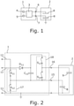
- Fig. 1 shows a power supply arrangement 1 connected to a plasma reactor 2.
- the plasma reactor 2 may be a plasma chamber. Inside the plasma reactor 2 a substrate can be processed. Either a layer of the substrate can be etched, or a layer can be deposited on the substrate.
- the power supply arrangement 1 comprises a pulsing assembly 3 connected to two power sources 4, 5 and has two power outputs 6, 7, which are connected to a first load 8 and a second load 9 of the plasma reactor 2.
- Fig. 2 shows a first embodiment of a pulsing assembly 3.
- the pulsing assembly 3 has a first pulsing unit 17 comprising a high side switch S11 and a low side switch S12.
- the switches S11, S12 are connected in series.
- the first pulsing unit 17 is connected to a common port 11 and a first input port 13.
- the first input port 13 and the common port 11 are configured to be connected to the first power source 4.
- the common port 11 is connected to ground.
- the pulsing assembly 3 furthermore has a second pulsing unit 18 comprising a high side switch S13 and a low side switch S14.
- the switches S13, S14 are connected in series.
- the second pulsing unit 18 is connected to an output port 15 of the first pulsing unit 17 and a second input port 12 via a rectifying component D11 embodied as a diode.
- the second input port 12 is configured to be connected to the second power source 5.
- the common port 11 is also configured to be connected to the second power source 5.
- the output port 15 of the first pulsing unit 17 is connected to the connection point of the switches S11, S12.
- the output port 15 is configured to be connected to the first load 8 of the plasma reactor 2, in particular via the output port 7 of the power supply arrangement 1 (output port 15 of the first pulsing unit 17 is connected to the output 7 of the power supply arrangement 1).
- the second pulsing unit 18 also comprises an output port 16, which is connected to the connection point of the switches S13, S14.
- the output port 16 is configured to be connected to the second load 9 of the plasma reactor 2, in particular via the output port 6 of the power supply arrangement 1 (output port 16 of the second pulsing unit 18 is connected to the output 6 of the power supply arrangement 1).
- An energy storage component C11 in this case embodied as capacitor, is connected to the output port 15 and the high side switch S13 and/or to input port 12 of the second pulsing unit 18 by rectifying component D11.
- switch S12 When switch S12 is switched on, the capacitive load 8 is discharged. At the same time the energy storage component C11 is charged to the voltage between ports 12 and 11 by rectifying component D11 and switch S12. This corresponds to a second pulsing time period. Usually, the voltage at the output port 16 should change in the same way as the voltage on the capacitive load 9, therefore switch S14 in the second pulsing unit 18 may be operated together with switch S12. Capacitive load 9 is discharged by switches S14 and S12. In order to supply the load 8 with the voltage of first input port 13, the switch S11 is switched on (and switch S12 is switched off). The load 8 is then charged to the voltage at input port 13 by switch S11.
- Fig 3 shows a second embodiment of a pulsing assembly 3, which corresponds to the pulsing assembly of Fig. 2 . Therefore, the same reference signs are being used. The only difference is that the polarity of the power sources 4, 5 is reversed.
- Fig. 4 shows in bold lines current paths for the state of discharging the capacitive loads 8, 9 of plasma reactor 2. To this end the switches S12 and S14 are closed and switches S11 and S13 are open. At the same time energy storage component C11 is charged via rectifying component D11 and switch S12 to the voltage at input port 12. This state corresponds to a second pulsing time period.
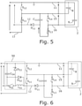
- Fig. 5 shows in bold lines the current paths for the state of pulse generation.
- Capacitive load 8 is charged via switch S11 to the voltage at input port 13.
- Load 9 is charged to voltage at output port 16 by switch S13.
- Energy for this charging comes from power source 4 and energy storage component C11, whose higher electrode is connected to output port 15.
- Rectifying component D11 is in blocking state, so voltage source 5 is disconnected from the circuit by this rectifying component.
- the situation shown in fig. 5 corresponds to the first and third pulsing time period.
- Figure 6 shows an embodiment of a pulsing assembly having a charging circuit 50 connected between second input port 12 and the second pulsing unit 18.
- Switches S13 and S14 can operate independently and the voltage on output 16 can be other than 0V
- the main advantage of the invention is to eliminate the need for a high voltage source and a high voltage pulsing unit to supply output port 16.
- the only extra high voltage element is a rectifying component D11 which is used to charge the energy storage component C11.
- Everything else to supply load 9 are low voltage elements: power source 5, pulsing unit 18 and energy storage component C11.
Landscapes
- Physics & Mathematics (AREA)
- Engineering & Computer Science (AREA)
- Plasma & Fusion (AREA)
- Chemical & Material Sciences (AREA)
- Analytical Chemistry (AREA)
- Plasma Technology (AREA)
- Generation Of Surge Voltage And Current (AREA)
Priority Applications (7)
| Application Number | Priority Date | Filing Date | Title |
|---|---|---|---|
| EP20461554.6A EP3945541A1 (de) | 2020-07-29 | 2020-07-29 | Impulsanordnung, stromversorgungsanordnung und verfahren mit der verwendung der impulsanordnung |
| PCT/EP2021/071165 WO2022023422A1 (en) | 2020-07-29 | 2021-07-28 | Pulsing assembly and power supply arrangement |
| EP21751566.7A EP4189724B1 (de) | 2020-07-29 | 2021-07-28 | Impulsanordnung, stromversorgungsanordnung und verfahren mit der verwendung der impulsanordnung |
| CN202180060454.6A CN116569304A (zh) | 2020-07-29 | 2021-07-28 | 脉冲发生组件和电源装置 |
| JP2023505889A JP7443620B2 (ja) | 2020-07-29 | 2021-07-28 | パルス化アセンブリ及び電力供給装置 |
| KR1020237003800A KR102845174B1 (ko) | 2020-07-29 | 2021-07-28 | 펄싱 어셈블리 및 전원 공급기 장치 |
| US18/160,315 US12322570B2 (en) | 2020-07-29 | 2023-01-27 | Pulsing assembly and power supply arrangement |
Applications Claiming Priority (1)
| Application Number | Priority Date | Filing Date | Title |
|---|---|---|---|
| EP20461554.6A EP3945541A1 (de) | 2020-07-29 | 2020-07-29 | Impulsanordnung, stromversorgungsanordnung und verfahren mit der verwendung der impulsanordnung |
Publications (1)
| Publication Number | Publication Date |
|---|---|
| EP3945541A1 true EP3945541A1 (de) | 2022-02-02 |
Family
ID=71894769
Family Applications (2)
| Application Number | Title | Priority Date | Filing Date |
|---|---|---|---|
| EP20461554.6A Withdrawn EP3945541A1 (de) | 2020-07-29 | 2020-07-29 | Impulsanordnung, stromversorgungsanordnung und verfahren mit der verwendung der impulsanordnung |
| EP21751566.7A Active EP4189724B1 (de) | 2020-07-29 | 2021-07-28 | Impulsanordnung, stromversorgungsanordnung und verfahren mit der verwendung der impulsanordnung |
Family Applications After (1)
| Application Number | Title | Priority Date | Filing Date |
|---|---|---|---|
| EP21751566.7A Active EP4189724B1 (de) | 2020-07-29 | 2021-07-28 | Impulsanordnung, stromversorgungsanordnung und verfahren mit der verwendung der impulsanordnung |
Country Status (6)
| Country | Link |
|---|---|
| US (1) | US12322570B2 (de) |
| EP (2) | EP3945541A1 (de) |
| JP (1) | JP7443620B2 (de) |
| KR (1) | KR102845174B1 (de) |
| CN (1) | CN116569304A (de) |
| WO (1) | WO2022023422A1 (de) |
Families Citing this family (1)
| Publication number | Priority date | Publication date | Assignee | Title |
|---|---|---|---|---|
| EP4738619A1 (de) | 2024-10-30 | 2026-05-06 | TRUMPF Huettinger Sp. Z o. o. | Hv-verbinder für industrielle stromausrüstung |
Citations (5)
| Publication number | Priority date | Publication date | Assignee | Title |
|---|---|---|---|---|
| EP0553410A1 (de) * | 1992-01-29 | 1993-08-04 | Leybold Aktiengesellschaft | Vorrichtung zum Beschichten eines Substrats, insbesondere mit elektrisch nichtleitenden Schichten |
| US20040055881A1 (en) * | 2002-09-25 | 2004-03-25 | Christie David J. | High peak power plasma pulsed supply with arc handling |
| WO2005005684A1 (en) * | 2003-07-10 | 2005-01-20 | Biocell Aktiebolag | Work piece processing by pulsed electric discharges in solid-gas plasma |
| WO2008071732A2 (en) * | 2006-12-12 | 2008-06-19 | Oc Oerlikon Balzers Ag | Rf substrate bias with high power impulse magnetron sputtering (hipims) |
| WO2019212592A1 (en) | 2018-05-03 | 2019-11-07 | Applied Materials, Inc. | Pulsed plasma (dc/rf) deposition of high quality c films for patterning |
Family Cites Families (44)
| Publication number | Priority date | Publication date | Assignee | Title |
|---|---|---|---|---|
| FR2547106B1 (fr) | 1983-05-30 | 1985-07-12 | Cem Comp Electro Mec | Dispositif d'equilibrage d'interrupteurs connectes en serie |
| FR2569067B1 (fr) | 1984-01-25 | 1986-12-05 | Jeumont Schneider | Montage en serie de transistors de puissance |
| US20020004309A1 (en) | 1990-07-31 | 2002-01-10 | Kenneth S. Collins | Processes used in an inductively coupled plasma reactor |
| US6488807B1 (en) | 1991-06-27 | 2002-12-03 | Applied Materials, Inc. | Magnetic confinement in a plasma reactor having an RF bias electrode |
| JPH06197522A (ja) | 1992-12-22 | 1994-07-15 | Toshiba Corp | 半導体スイッチ装置 |
| JP3036296B2 (ja) * | 1993-05-25 | 2000-04-24 | 富士通株式会社 | プラズマディスプレイ装置の電源装置 |
| JPH0767320A (ja) | 1993-08-25 | 1995-03-10 | Toshiba Fa Syst Eng Kk | 電力素子の駆動回路 |
| DE19651811B4 (de) * | 1996-12-13 | 2006-08-31 | Unaxis Deutschland Holding Gmbh | Vorrichtung zum Belegen eines Substrats mit dünnen Schichten |
| SG66453A1 (en) | 1997-04-23 | 1999-07-20 | Int Rectifier Corp | Resistor in series with bootstrap diode for monolithic gate device |
| DE19838389C1 (de) | 1998-08-24 | 2000-03-09 | Siemens Ag | Verfahren und Vorrichtung zur Steuerung eines abschaltbaren Stromrichterventils mit der Reihenschaltzahl Zwei oder größer |
| JP4101554B2 (ja) * | 2001-08-17 | 2008-06-18 | 株式会社神戸製鋼所 | スパッタ装置及び方法 |
| JP2004080891A (ja) | 2002-08-15 | 2004-03-11 | Origin Electric Co Ltd | 定電力電源装置、及びそれを用いてなるスパッタ装置 |
| JP2004103423A (ja) | 2002-09-10 | 2004-04-02 | Matsushita Electric Works Ltd | プラズマ処理方法及びプラズマ処理装置 |
| US6859087B2 (en) | 2002-10-31 | 2005-02-22 | International Rectifier Corporation | Half-bridge high voltage gate driver providing protection of a transistor |
| JP2004343899A (ja) | 2003-05-15 | 2004-12-02 | Toyota Motor Corp | プラズマ発生用電源装置および排ガス浄化システム |
| JP2005168275A (ja) | 2003-11-14 | 2005-06-23 | Sekisui Chem Co Ltd | プラズマ処理装置 |
| US6963498B2 (en) | 2004-02-02 | 2005-11-08 | International Rectifier Corporation | Bootstrap capacitor refresh circuit |
| JP5163207B2 (ja) | 2008-03-19 | 2013-03-13 | セイコーエプソン株式会社 | 液体噴射装置、及び印刷装置 |
| JP5037475B2 (ja) * | 2008-11-11 | 2012-09-26 | 株式会社神戸製鋼所 | スパッタ装置 |
| DE102009006154A1 (de) | 2009-01-26 | 2010-07-29 | Bergmann Meßgeräte Entwicklung KG | Hochspannungsschalter mit einstellbarem Strom |
| US8382999B2 (en) | 2009-03-26 | 2013-02-26 | Applied Materials, Inc. | Pulsed plasma high aspect ratio dielectric process |
| JP5520512B2 (ja) | 2009-04-09 | 2014-06-11 | 株式会社ソニー・コンピュータエンタテインメント | 情報処理装置および情報処理方法 |
| US8404598B2 (en) | 2009-08-07 | 2013-03-26 | Applied Materials, Inc. | Synchronized radio frequency pulsing for plasma etching |
| CN101984546B (zh) | 2010-02-05 | 2013-03-06 | 深圳市科陆变频器有限公司 | 功率开关器件串联限压电路 |
| DE102012021346A1 (de) * | 2012-11-01 | 2014-08-28 | Oerlikon Trading Ag, Trübbach | Leistungsverteiler zur definierten sequenziellen Leistungsverteilung |
| US9129776B2 (en) * | 2012-11-01 | 2015-09-08 | Advanced Energy Industries, Inc. | Differing boost voltages applied to two or more anodeless electrodes for plasma processing |
| DE102012222606A1 (de) | 2012-12-10 | 2014-06-26 | Trumpf Laser Gmbh + Co. Kg | Pockelszellentreiberschaltung und Verfahren zum Betrieb einer Pockelszelle |
| DE102013212099B4 (de) | 2013-06-25 | 2020-03-05 | Trumpf Laser Gmbh | Hochspannungsmodulation ohne Schleppfehler |
| CN203504399U (zh) | 2013-09-16 | 2014-03-26 | 王达开 | 一种功率开关器件串联限压电路 |
| JP2015136197A (ja) | 2014-01-16 | 2015-07-27 | 株式会社リコー | インバータ装置とプラズマ発生装置及びシート材改質装置 |
| EP2988403B1 (de) | 2014-08-19 | 2019-10-02 | General Electric Technology GmbH | Halbleiterschaltstrang |
| US9779919B2 (en) | 2015-01-09 | 2017-10-03 | Hitachi High-Technologies Corporation | Plasma processing apparatus and plasma processing method |
| CN105406722B (zh) | 2015-12-18 | 2018-10-02 | 北京理工大学 | 二极管钳位功率开关串联高压直流变压器 |
| CN105356779B (zh) | 2015-12-18 | 2018-09-21 | 北京理工大学 | 一种二极管钳位功率开关串联高压逆变器及其拓扑结构 |
| DE102016223314A1 (de) | 2016-11-24 | 2018-05-24 | Trumpf Laser Gmbh | Treiberschaltung, insbesondere für eine Pockelszelle und Verfahren zum Betrieb einer Treiberschaltung |
| EP3396700A1 (de) * | 2017-04-27 | 2018-10-31 | TRUMPF Hüttinger GmbH + Co. KG | Strommwandlungseinheit, plasmaverarbeitungsausrüstung und verfahren zur steuerung mehrerer plasmaprozesse |
| CN110771022B (zh) | 2017-06-12 | 2023-05-02 | 星火工业有限公司 | 具有用于磁控溅射的脉冲和离子通量控制的脉冲功率模块 |
| JP7565079B2 (ja) | 2017-09-07 | 2024-10-10 | ヴィスアイシー テクノロジーズ リミテッド | 高電圧高速スイッチング装置 |
| US10763150B2 (en) | 2017-09-20 | 2020-09-01 | Applied Materials, Inc. | System for coupling a voltage to spatially segmented portions of the wafer with variable voltage |
| US10714372B2 (en) | 2017-09-20 | 2020-07-14 | Applied Materials, Inc. | System for coupling a voltage to portions of a substrate |
| JP7033907B2 (ja) | 2017-12-21 | 2022-03-11 | 東京エレクトロン株式会社 | プラズマエッチング装置及びプラズマエッチング方法 |
| US10347500B1 (en) | 2018-06-04 | 2019-07-09 | Applied Materials, Inc. | Device fabrication via pulsed plasma |
| US11398369B2 (en) * | 2019-06-25 | 2022-07-26 | Applied Materials, Inc. | Method and apparatus for actively tuning a plasma power source |
| US11776788B2 (en) * | 2021-06-28 | 2023-10-03 | Applied Materials, Inc. | Pulsed voltage boost for substrate processing |
-
2020
- 2020-07-29 EP EP20461554.6A patent/EP3945541A1/de not_active Withdrawn
-
2021
- 2021-07-28 JP JP2023505889A patent/JP7443620B2/ja active Active
- 2021-07-28 KR KR1020237003800A patent/KR102845174B1/ko active Active
- 2021-07-28 WO PCT/EP2021/071165 patent/WO2022023422A1/en not_active Ceased
- 2021-07-28 CN CN202180060454.6A patent/CN116569304A/zh active Pending
- 2021-07-28 EP EP21751566.7A patent/EP4189724B1/de active Active
-
2023
- 2023-01-27 US US18/160,315 patent/US12322570B2/en active Active
Patent Citations (5)
| Publication number | Priority date | Publication date | Assignee | Title |
|---|---|---|---|---|
| EP0553410A1 (de) * | 1992-01-29 | 1993-08-04 | Leybold Aktiengesellschaft | Vorrichtung zum Beschichten eines Substrats, insbesondere mit elektrisch nichtleitenden Schichten |
| US20040055881A1 (en) * | 2002-09-25 | 2004-03-25 | Christie David J. | High peak power plasma pulsed supply with arc handling |
| WO2005005684A1 (en) * | 2003-07-10 | 2005-01-20 | Biocell Aktiebolag | Work piece processing by pulsed electric discharges in solid-gas plasma |
| WO2008071732A2 (en) * | 2006-12-12 | 2008-06-19 | Oc Oerlikon Balzers Ag | Rf substrate bias with high power impulse magnetron sputtering (hipims) |
| WO2019212592A1 (en) | 2018-05-03 | 2019-11-07 | Applied Materials, Inc. | Pulsed plasma (dc/rf) deposition of high quality c films for patterning |
Also Published As
| Publication number | Publication date |
|---|---|
| EP4189724B1 (de) | 2024-05-22 |
| KR20230028558A (ko) | 2023-02-28 |
| KR102845174B1 (ko) | 2025-08-11 |
| JP2023536110A (ja) | 2023-08-23 |
| US20230170184A1 (en) | 2023-06-01 |
| CN116569304A (zh) | 2023-08-08 |
| JP7443620B2 (ja) | 2024-03-05 |
| US12322570B2 (en) | 2025-06-03 |
| EP4189724A1 (de) | 2023-06-07 |
| EP4189724C0 (de) | 2024-05-22 |
| WO2022023422A1 (en) | 2022-02-03 |
Similar Documents
| Publication | Publication Date | Title |
|---|---|---|
| US20110074489A1 (en) | Inverter | |
| CN101124714B (zh) | 采用固态开关的高压脉冲电源 | |
| US6184741B1 (en) | Bidirectional charge pump generating either a positive or negative voltage | |
| US10855262B2 (en) | Systems and method for paralleled identical marx generators | |
| JP6691191B2 (ja) | 異常エネルギー保護付き電源変換システム及びその動作方法 | |
| CN112803572B (zh) | 具备故障重构功能的卫星电源系统 | |
| US10587188B2 (en) | Resonant pulsed voltage multiplier and capacitor charger | |
| EP4604377A1 (de) | Tief-hochsetz-wandler und stromversorgungssystem | |
| EP1543175B1 (de) | Gepulste plasmaenergieversorgung mit hoher spitzenleistung mit lichtbogenhandhabung | |
| EP4189724B1 (de) | Impulsanordnung, stromversorgungsanordnung und verfahren mit der verwendung der impulsanordnung | |
| US11888414B2 (en) | Driving circuit and driving method | |
| US20190319473A1 (en) | Energy storage system and method for direct coupling energy storage and power source | |
| JP5868401B2 (ja) | 交流電力を供給してプラズマを点火するための点火回路 | |
| CN115483675B (zh) | 电源切换装置及多输入电源 | |
| US20210111534A1 (en) | Driver circuit for laser diodes and circuit arrangement with such a driver circuit and laser diodes | |
| CN103855761B (zh) | 电动助力转向继电器的直流链电容器充放电控制装置及其方法 | |
| CN118523591B (zh) | 多种负载装备混合复用的脉冲电源拓扑结构及控制方法 | |
| US20260135377A1 (en) | Device and method for the voltage equalization of a plurality of two-terminal networks, and dc power distribution system | |
| EP4181350B1 (de) | Ladeanordnung für solarverfolger | |
| CN218243333U (zh) | 适用于安全防护的驱动电路 | |
| EP4181346A1 (de) | Solarbetriebenes batteriesystem mit mehrpegelwandler für traktionsstromnetze | |
| CN116774624A (zh) | 一种用于tvs可靠触发的双反馈控制电路 | |
| Kumar et al. | Design and Analysis of Dual Input DC-DC Converter for Integration of Multiple Energy Sources | |
| CN116964889A (zh) | 充电系统、电压转换器单元和存储单元 | |
| CN120768095A (zh) | 一种基于多级h桥级联的电压发生电路及其电压控制方法 |
Legal Events
| Date | Code | Title | Description |
|---|---|---|---|
| PUAI | Public reference made under article 153(3) epc to a published international application that has entered the european phase |
Free format text: ORIGINAL CODE: 0009012 |
|
| STAA | Information on the status of an ep patent application or granted ep patent |
Free format text: STATUS: THE APPLICATION HAS BEEN PUBLISHED |
|
| AK | Designated contracting states |
Kind code of ref document: A1 Designated state(s): AL AT BE BG CH CY CZ DE DK EE ES FI FR GB GR HR HU IE IS IT LI LT LU LV MC MK MT NL NO PL PT RO RS SE SI SK SM TR |
|
| STAA | Information on the status of an ep patent application or granted ep patent |
Free format text: STATUS: THE APPLICATION IS DEEMED TO BE WITHDRAWN |
|
| 18D | Application deemed to be withdrawn |
Effective date: 20220803 |