EP3948667B1 - Verbesserte karte mit fingerabdruckbiometriken - Google Patents
Verbesserte karte mit fingerabdruckbiometriken Download PDFInfo
- Publication number
- EP3948667B1 EP3948667B1 EP20784246.9A EP20784246A EP3948667B1 EP 3948667 B1 EP3948667 B1 EP 3948667B1 EP 20784246 A EP20784246 A EP 20784246A EP 3948667 B1 EP3948667 B1 EP 3948667B1
- Authority
- EP
- European Patent Office
- Prior art keywords
- sheet
- lead frame
- module
- contact pads
- opening
- Prior art date
- Legal status (The legal status is an assumption and is not a legal conclusion. Google has not performed a legal analysis and makes no representation as to the accuracy of the status listed.)
- Active
Links
Images


Classifications
-
- G—PHYSICS
- G06—COMPUTING OR CALCULATING; COUNTING
- G06K—GRAPHICAL DATA READING; PRESENTATION OF DATA; RECORD CARRIERS; HANDLING RECORD CARRIERS
- G06K19/00—Record carriers for use with machines and with at least a part designed to carry digital markings
- G06K19/06—Record carriers for use with machines and with at least a part designed to carry digital markings characterised by the kind of the digital marking, e.g. shape, nature, code
- G06K19/067—Record carriers with conductive marks, printed circuits or semiconductor circuit elements, e.g. credit or identity cards also with resonating or responding marks without active components
- G06K19/07—Record carriers with conductive marks, printed circuits or semiconductor circuit elements, e.g. credit or identity cards also with resonating or responding marks without active components with integrated circuit chips
- G06K19/0716—Record carriers with conductive marks, printed circuits or semiconductor circuit elements, e.g. credit or identity cards also with resonating or responding marks without active components with integrated circuit chips at least one of the integrated circuit chips comprising a sensor or an interface to a sensor
- G06K19/0718—Record carriers with conductive marks, printed circuits or semiconductor circuit elements, e.g. credit or identity cards also with resonating or responding marks without active components with integrated circuit chips at least one of the integrated circuit chips comprising a sensor or an interface to a sensor the sensor being of the biometric kind, e.g. fingerprint sensors
-
- G—PHYSICS
- G06—COMPUTING OR CALCULATING; COUNTING
- G06K—GRAPHICAL DATA READING; PRESENTATION OF DATA; RECORD CARRIERS; HANDLING RECORD CARRIERS
- G06K19/00—Record carriers for use with machines and with at least a part designed to carry digital markings
- G06K19/06—Record carriers for use with machines and with at least a part designed to carry digital markings characterised by the kind of the digital marking, e.g. shape, nature, code
- G06K19/067—Record carriers with conductive marks, printed circuits or semiconductor circuit elements, e.g. credit or identity cards also with resonating or responding marks without active components
- G06K19/07—Record carriers with conductive marks, printed circuits or semiconductor circuit elements, e.g. credit or identity cards also with resonating or responding marks without active components with integrated circuit chips
- G06K19/073—Special arrangements for circuits, e.g. for protecting identification code in memory
- G06K19/07309—Means for preventing undesired reading or writing from or onto record carriers
- G06K19/07345—Means for preventing undesired reading or writing from or onto record carriers by activating or deactivating at least a part of the circuit on the record carrier, e.g. ON/OFF switches
- G06K19/07354—Means for preventing undesired reading or writing from or onto record carriers by activating or deactivating at least a part of the circuit on the record carrier, e.g. ON/OFF switches by biometrically sensitive means, e.g. fingerprint sensitive
-
- B—PERFORMING OPERATIONS; TRANSPORTING
- B42—BOOKBINDING; ALBUMS; FILES; SPECIAL PRINTED MATTER
- B42D—BOOKS; BOOK COVERS; LOOSE LEAVES; PRINTED MATTER CHARACTERISED BY IDENTIFICATION OR SECURITY FEATURES; PRINTED MATTER OF SPECIAL FORMAT OR STYLE NOT OTHERWISE PROVIDED FOR; DEVICES FOR USE THEREWITH AND NOT OTHERWISE PROVIDED FOR; MOVABLE-STRIP WRITING OR READING APPARATUS
- B42D25/00—Information-bearing cards or sheet-like structures characterised by identification or security features; Manufacture thereof
- B42D25/20—Information-bearing cards or sheet-like structures characterised by identification or security features; Manufacture thereof characterised by a particular use or purpose
- B42D25/23—Identity cards
-
- B—PERFORMING OPERATIONS; TRANSPORTING
- B42—BOOKBINDING; ALBUMS; FILES; SPECIAL PRINTED MATTER
- B42D—BOOKS; BOOK COVERS; LOOSE LEAVES; PRINTED MATTER CHARACTERISED BY IDENTIFICATION OR SECURITY FEATURES; PRINTED MATTER OF SPECIAL FORMAT OR STYLE NOT OTHERWISE PROVIDED FOR; DEVICES FOR USE THEREWITH AND NOT OTHERWISE PROVIDED FOR; MOVABLE-STRIP WRITING OR READING APPARATUS
- B42D25/00—Information-bearing cards or sheet-like structures characterised by identification or security features; Manufacture thereof
- B42D25/30—Identification or security features, e.g. for preventing forgery
- B42D25/305—Associated digital information
-
- B—PERFORMING OPERATIONS; TRANSPORTING
- B42—BOOKBINDING; ALBUMS; FILES; SPECIAL PRINTED MATTER
- B42D—BOOKS; BOOK COVERS; LOOSE LEAVES; PRINTED MATTER CHARACTERISED BY IDENTIFICATION OR SECURITY FEATURES; PRINTED MATTER OF SPECIAL FORMAT OR STYLE NOT OTHERWISE PROVIDED FOR; DEVICES FOR USE THEREWITH AND NOT OTHERWISE PROVIDED FOR; MOVABLE-STRIP WRITING OR READING APPARATUS
- B42D25/00—Information-bearing cards or sheet-like structures characterised by identification or security features; Manufacture thereof
- B42D25/40—Manufacture
- B42D25/45—Associating two or more layers
- B42D25/455—Associating two or more layers using heat
-
- B—PERFORMING OPERATIONS; TRANSPORTING
- B42—BOOKBINDING; ALBUMS; FILES; SPECIAL PRINTED MATTER
- B42D—BOOKS; BOOK COVERS; LOOSE LEAVES; PRINTED MATTER CHARACTERISED BY IDENTIFICATION OR SECURITY FEATURES; PRINTED MATTER OF SPECIAL FORMAT OR STYLE NOT OTHERWISE PROVIDED FOR; DEVICES FOR USE THEREWITH AND NOT OTHERWISE PROVIDED FOR; MOVABLE-STRIP WRITING OR READING APPARATUS
- B42D25/00—Information-bearing cards or sheet-like structures characterised by identification or security features; Manufacture thereof
- B42D25/40—Manufacture
- B42D25/45—Associating two or more layers
- B42D25/46—Associating two or more layers using pressure
-
- G—PHYSICS
- G06—COMPUTING OR CALCULATING; COUNTING
- G06K—GRAPHICAL DATA READING; PRESENTATION OF DATA; RECORD CARRIERS; HANDLING RECORD CARRIERS
- G06K19/00—Record carriers for use with machines and with at least a part designed to carry digital markings
- G06K19/06—Record carriers for use with machines and with at least a part designed to carry digital markings characterised by the kind of the digital marking, e.g. shape, nature, code
- G06K19/067—Record carriers with conductive marks, printed circuits or semiconductor circuit elements, e.g. credit or identity cards also with resonating or responding marks without active components
- G06K19/07—Record carriers with conductive marks, printed circuits or semiconductor circuit elements, e.g. credit or identity cards also with resonating or responding marks without active components with integrated circuit chips
- G06K19/077—Constructional details, e.g. mounting of circuits in the carrier
- G06K19/07749—Constructional details, e.g. mounting of circuits in the carrier the record carrier being capable of non-contact communication, e.g. constructional details of the antenna of a non-contact smart card
- G06K19/07773—Antenna details
-
- G—PHYSICS
- G06—COMPUTING OR CALCULATING; COUNTING
- G06V—IMAGE OR VIDEO RECOGNITION OR UNDERSTANDING
- G06V40/00—Recognition of biometric, human-related or animal-related patterns in image or video data
- G06V40/10—Human or animal bodies, e.g. vehicle occupants or pedestrians; Body parts, e.g. hands
- G06V40/12—Fingerprints or palmprints
- G06V40/13—Sensors therefor
Definitions
- This application relates to an improved card with fingerprint biometrics.
- the card can be used to identify securely an individual using biometric analysis.
- the card has a processor with an internal memory and a biometric sensor.
- a user connects the card to a scanner directly using physical electrical contacts or remotely using an electromagnetic interface.
- the memory often stores data for the purpose of encryption.
- the biometric sensor is intended for obtaining a physical trait of the user, namely fingerprint.
- US2019/019005A1 shows a flexible electronic card that includes a card body, at least one cavity formed in the card body, and a fingerprint module configured to acquire a fingerprint of a user.
- EP3336759A1 shows a fingerprint sensing module that includes a fingerprint sensor device having a sensing array arranged on a side of the device, and connection pads for connecting the fingerprint sensor device to external circuitry and a fingerprint sensor device cover structure.
- KR20180123085A shows a method of manufacturing a smart card.
- US2014/124583A1 shows a smart card that comprises a top layer, a core layer of thermoset polymeric material, and a bottom layer comprising an Integrated Electronics Assembly.
- US2007/235548A1 shows an electronic inlay that includes a circuit board, a plurality of circuit components attached to the circuit board, a bottom cover sheet, a top cover sheet, and a layer of thermosetting material between the bottom and top cover sheets.
- KR101706592B1 shows a fingerprint recognition radio-frequency (RF) smart card with an enhanced security function.
- the fingerprint recognition RF smart card has a CPU directly connected to a combination chip to execute a control operation, thereby preventing card information stored in the combination chip from being transmitted to the outside when the fingerprint information measured by a fingerprint sensor does not match the fingerprint information of a user.
- US2013/207786A1 shows a passive secure data card that is provided with biometric authorization.
- the application provides an inlay for a biometric card.
- the inlay includes a first transparent overlay sheet, an antenna carrier sheet, a thickness compensation sheet, and a second transparent overlay sheet, and several components.
- the antenna carrier sheet is provided next to the first transparent overlay sheet, and it includes a microcontroller opening, a contact module lead frame opening, and a finger sensor lead frame opening.
- the thickness compensation sheet is provided next to the first transparent overlay sheet.
- the second transparent overlay sheet is provided next to the thickness compensation sheet.
- the components include a microcontroller, a module lead frame, a finger sensor lead frame, an antenna, and a plurality of electrical wires.
- the microcontroller is also called a processing module, such as a secure processing module. It is placed in the microcontroller opening.
- the module lead frame is adapted for being milled or cut, and it is placed in the contact module lead frame opening.
- the module lead frame comprises a plurality of first contact pads for contacting a card contact module.
- the lead frame refers to a metal structure for carrying an electrical signal from one part of the lead frame to another part of the lead frame.
- the card contact module is intended for contacting a card reader to exchanged information with the card reader.
- the finger sensor lead frame is adapted for being milled or cut, and it is provided in the sensor lead frame opening.
- the sensor lead frame comprising a plurality of second contact pads for contacting a fingerprint sensor.
- the antenna includes a coil of an electrical conductor being embedded in the antenna carrier sheet.
- the antenna is intended for receiving energy or signal from an external source and for transmitting the energy or signal to electrical components of the card.
- the electrical wires are electrically connected to electric contact pads of the microcontroller, to the first contact pads, to the second contact pads, and to the electrical conductor of the antenna.
- This inlay allows easy change of electrical connections between electrical components. In other words, a user can another finger sensor or contact module with different pin out with only a little effort to assign the electrical wires to different pins.
- One or more electrical wire can overlap with another electrical wire. This overlap allows flexible arrangement of electrical wires.
- An intermediate transparent PVC sheet can be provided next to the second transparent overlay sheet.
- the inlay can include one or more additional sheet or layer.
- the additional sheet enables the inlay to have different properties to meet different needs of use, such as additional layers for enhanced protection.
- the application provides a method of producing an inlay.
- the method includes a step of providing an antenna carrier sheet.
- the antenna carrier sheet is milled, cut, or punched to provide the antenna carrier sheet with several openings, namely a first opening, a second opening, and a third opening.
- the first opening is intended for receiving a part of the microcontroller, namely a printed circuit board of the microcontroller.
- the first opening is adapted for receiving the printed circuit board.
- the second opening is intended for receiving a module lead frame while the third opening is intended for receiving a sensor lead frame.
- An adhesive tape is then placed next to the antenna carrier sheet such that the antenna carrier sheet is attached to an adhesive layer of the adhesive tape.
- the antenna carrier sheet is later placed on a supporting surface, wherein the adhesive tape is resting on the supporting surface. This is to allow easy placement of parts into the openings of the antenna carrier sheet.
- the printed circuit board is afterward inserted into the first opening, wherein the printed circuit board is attached to the adhesive tape.
- the module lead frame is inserted into the second opening such that the module lead frame is attached to the adhesive tape.
- the sensor lead frame is inserted into the third opening, wherein the sensor lead frame is attached to the adhesive tape.
- the adhesive tape then keeps the printed circuit board, the module lead frame, and the sensor lead frame from moving with respect to the adhesive tape.
- An antenna comprising a coil of an electrical conductor is later embedded in the antenna carrier sheet.
- the embedding fixes the coil of the electrical conductor to the antenna carrier sheet. In a general sense, this step of embedding can be also be done before or after the above step of placing the adhesive tape next to the antenna carrier sheet.
- a plurality of electrical wires is afterwards attached to electrical contact pads of the printed circuit board, to electrical contact pads of the module lead frame, to electrical contact pads of the sensor lead frame, and to the electrical conductor of the antenna.
- a thickness compensation sheet is provided with an opening to receive a moulded part of the microcontroller.
- the printed circuit board is electrically attached to one or more semiconductor chips while the moulded part covers and protects the semiconductor chips.
- the thickness compensation sheet is then placed next to the antenna carrier sheet such that the opening receives the moulded part of the microcontroller.
- the adhesive tape is afterwards removed from the antenna carrier sheet.
- a first transparent overlay sheet is afterwards provided next to the antenna carrier sheet.
- the first transparent overlay sheet touches the antenna carrier sheet.
- a second transparent overlay sheet is also placed next to the thickness compensation sheet, wherein the second transparent overlay sheet touches the thickness compensation sheet. This step can be done before or after the step of removing the adhesive tape from the antenna carrier sheet.
- the first transparent overlay sheet, the antenna carrier sheet, the thickness compensation sheet, and the second transparent overlay sheet are then laminated, wherein these sheets are pressed against each other to form the complete or final inlay 12.
- the method can include a further step of providing an intermediate transparent PVC sheet next to the second transparent overlay sheet.
- the intermediate transparent PVC sheet then touches the second transparent overlay sheet.
- the application provides a biometric card.
- the card includes an inlay.
- the inlay comprises a first transparent overlay sheet, an antenna carrier sheet, a thickness compensation sheet, a second transparent overlay sheet, a microcontroller, first contact pads of a module lead frame, second contact pads of a sensor lead frame, an antenna, and a plurality of electrical wires.
- the antenna carrier sheet is provided next to the first transparent overlay sheet and it comprises a microcontroller opening, a module lead frame opening, and a sensor lead frame opening.
- the thickness compensation sheet is provided next to the first transparent overlay sheet.
- the second transparent overlay sheet is provided next to the thickness compensation sheet.
- the microcontroller is provided in the microcontroller opening.
- the first contact pads of the module lead frame are provided in the module lead frame opening.
- the second contact pads of the sensor lead frame are provided in the sensor lead frame opening.
- the antenna includes a coil of electrical conductor being embedded in the antenna carrier sheet.
- the electrical wires are electrically connected to contact pads of the microcontroller, to the first contact pads, to the second contact pads, and to the electrical conductor of the antenna.
- the card also includes a first printed PVC sheet, a first transparent PVC sheet, a second printed PVC sheet, a second transparent PVC sheet, a fingerprint sensor, and a contact module.
- the first printed PVC sheet is provided next to a first transparent overlay sheet of the inlay.
- the first transparent PVC sheet is provided next to the first printed PVC sheet.
- the second printed PVC sheet is provided next a second transparent overlay sheet of the inlay.
- the second printed PVC sheet is provided next to the intermediate transparent PVC sheet.
- the second transparent PVC sheet is provided next to the second printed PVC sheet.
- the first transparent PVC sheet, the first printed PVC sheet, and the first transparent overlay sheet comprise a contact module opening and a fingerprint sensor opening.
- the contact module is provided in the contact module opening and it is electrically connected to the first contact pads.
- the fingerprint sensor is provided in the fingerprint sensor opening and it is electrically connected to the second contact pads.
- An intermediate transparent PVC sheet can be provided between the second transparent overlay sheet and the second printed PVC sheet.
- One or more electrical wires can overlap with another electrical wire.
- the card often includes a first electrically conductive substance for electrically connecting the contact module to the first contact pads.
- the card often includes a second electrically conductive substance for electrically connecting the fingerprint sensor to the second contact pads.
- the application provides a method of producing a card.
- the method includes a step of providing the above-mentioned inlay.
- a first printed PVC sheet is then provided next to a first transparent overlay sheet of the inlay. After this, a first transparent PVC sheet is provided next to the first transparent PVC sheet.
- a second printed PVC sheet is later provided next to a second transparent overlay sheet of the inlay. Following this, a second transparent PVC sheet is provided next to the second printed PVC sheet.
- the second printed PVC sheet can be provided before or after the step of providing the first printed PVC sheet.
- a first major surface of the first transparent PVC sheet is afterwards milled or cut such that a module lead frame body of a module lead frame is electrically detached from module lead frame contact pads of the module lead frame.
- the module lead frame contact pads are electrically isolated from each other.
- the first major surface is milled or cut such that a sensor lead frame body of a sensor lead frame is electrically detached from sensor lead frame contact pads of the sensor lead frame.
- the sensor lead frame contact pads are electrically isolated from each other.
- the first major surface is milled or cut for providing a first recess to receive a contact module.
- the first major surface is also milled or cut for providing a second recess to receive a fingerprint sensor.
- the above-mentioned steps of milling can be done different orders or sequences.
- the step of detaching the module lead frame contact pads from each other can be done before or after the step of detaching the sensor lead frame contact pads from each other.
- the step of milling to provide the first recess can be done before or after the step of milling to provide the second recess.
- the step of milling to provide the first or second recess can be done before or after the step of detaching the module lead frame contact pads or detaching the sensor lead frame contact pads from each other.
- the method often includes a step of inserting a contact module into the first recess, wherein the contact module is electrically connected to the module lead frame contact pads and a step of inserting a fingerprint sensor into the second recess, wherein the fingerprint sensor is electrically connected to the sensor lead frame contact pads.
- a first electrically conductive substance is often provided to electrically connect the contact module to the module lead frame contact pads.
- a second electrically conductive substance is often provided to electrically connect the fingerprint sensor to the sensor lead frame contact pads.
- Some parts of the embodiments have similar parts.
- the similar parts may have the same names or the similar part numbers with an alphabet symbol.
- the description of one similar part also applies by reference to another similar part, where appropriate, thereby reducing repetition of text without limiting the disclosure.
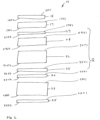
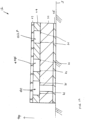
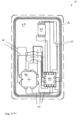
- Fig. 1 shows a card 10 with fingerprint biometrics.
- the card 10 includes an improved inlay 12, a plurality of flat sheets, and a plurality of electronic modules.
- the inlay 12 and the flat sheets have essentially the same rectangular shape.
- the inlay 12 and the flat sheets are arranged in a stack, wherein an outer edge of the inlay 12 is placed next to outer edges of the flat sheets.
- the inlay 12 is positioned between the flat sheets.
- the electronic modules are embedded in the flat sheets and in the inlay 12.
- the flat sheets include a first transparent polyvinyl chloride (PVC) sheet 15, a first printed PVC sheet 17, an intermediate transparent PVC sheet 20, and a second printed PVC sheet 23, and a second transparent PVC sheet 25.
- PVC polyvinyl chloride
- a first major surface 15S1 of the first transparent PVC sheet 15 acts as an external surface of the chip 10 that a user can touch.
- a second major surface 15S2 of the first transparent PVC sheet 15 is placed next to a first major surface 17S1 of the first printed PVC sheet 17.
- the second major surface 15S1 is positioned opposite the first major surface 15S2.
- a second major surface 17S2 of the first printed PVC sheet 17 is placed next to a first major surface of the inlay 12.
- the second major surface 17S2 is positioned opposite the first major surface 17S1.
- a second major surface of the inlay 12 is placed next to a first major surface 20S1 of the intermediate transparent PVC sheet 20.
- the second major surface of the inlay 12 is positioned opposite the first major surface of the inlay 12.
- a second major surface 20S2 of the intermediate transparent PVC sheet 20 is placed next to a first major surface 23S1 of the second printed PVC sheet 23.
- the second major surface 20S2 is positioned opposite the first major surface 20S1.
- a second major surface 23S2 of the second printed PVC sheet 23 is placed next to a first major surface 25S1 of the second transparent PVC sheet 25.
- the second major surface 23S2 is positioned opposite the first major surface 23S1.
- a second major surface 25S2 of the second transparent PVC sheet 25 acts as an external surface of the chip 10 that a user can touch.
- the second major surface 25S2 is positioned opposite the first major surface 25S1.
- the inlay 12 includes a first transparent overlay sheet 27, an antenna carrier sheet 29, a thickness compensation sheet 32, a second transparent overlay sheet 35.
- the antenna carrier sheet 29 is also called an antenna sheet.
- a first major surface 27S1 of the first transparent overlay sheet 27 is placed next to the second major surface 17S2 of the first printed PVC sheet 17.
- a second major surface 27S2 of the first transparent overlay sheet 27 is placed next to a first major surface 29S1 of the antenna carrier sheet 29.
- the second major surface 27S2 is positioned opposite the first major surface 27S1.
- a second major surface 29S2 of the antenna carrier sheet 29 is placed next to a first major surface 32S1 of the thickness compensation sheet 32.
- the second major surface 29S2 is positioned opposite the first major surface 29S1.
- a second major surface 32S2 of the thickness compensation sheet 32 is placed next to a first major surface 35S1 of the second transparent overlay sheet 35.
- the second major surface 32S2 is positioned opposite the first major surface 32S1.
- a second major surface 35S2 of the second transparent overlay sheet 35 is placed next to the first major surface 20S1 of the intermediate transparent PVC sheet 20.
- the second major surface 35S2 is position opposite the first major surface 35S1.
- the electronic modules include a secure processing module 40, a contact module 43 with contact pads 43CP of a millable module lead frame, a fingerprint sensor 46 with lead frame contact pads 46CP of a millable sensor lead frame, and a plurality of module electrical wires W.
- the secure processing module 40 is also called a computing processor or a microcontroller.
- the module lead frame and the sensor lead frame are adapted for milled or cut. In other words, the material and design of the module lead frame and the sensor lead frame are selected such that the module lead frame and the sensor lead frame are suitable for being milled.
- the secure processing module 40 it includes a printed circuit board (PCB) 40PCB and a moulded part 40MP. One end of the moulded part 40MP is attached to a surface of the PCB 40PCB.
- PCB printed circuit board
- the PCB 40PCB includes an essentially rectangular sheet, one or more semiconductor chips, and several electrical contact pads.
- the rectangular sheet of the PCB 40PCB comprises a composite material that is flame resistant.
- the composite material includes a woven fiberglass cloth with an epoxy resin binder.
- the electrical contact pads are placed on outer parts or edges of a contact surface of the rectangular sheet.
- the semiconductor chips are placed on an inner or central part of the above-mentioned contact surface of the rectangular sheet of the PCB 40PCB.
- the semiconductor chips are electrically connected to the electrical contact pads via a plurality of chip electrical wires.
- the moulded part 40MP has a shape essentially of a rectangular block.
- the moulded part 40MP is attached to the contact surface of the rectangular sheet of the PCB 40PCB and it encapsulates and covers the semiconductor chips.
- the rectangular sheet of the PCB 40PCB and the antenna carrier sheet 29 have about the same thickness.
- the moulded part 40MP has a height that is about the same as the thickness of the compensation sheet 32.
- the rectangular sheet of the PCB 40PCB is inserted in an opening of the antenna carrier sheet 29 while the moulded part 40MP is inserted in an opening of the compensation sheet 32.
- the insertion is done such that the contact surface of the rectangular sheet is aligned with the second major surface 29S2 of the antenna carrier sheet 29.
- the contact module 43 has a shape essentially of a rectangular block.
- the contact module 43 has a first surface and a second surface that is placed opposite the first surface.
- the first surface includes a plurality of external module contact pads.
- the second surface includes a plurality of inner module contact pads.
- the external module contact pads are adapted for contacting electrical terminals of a card reader (not shown here).
- the contact module 43 is inserted in an opening of the first transparent PVC sheet 15, an opening of the first printed PVC sheet 17, and an opening of the first transparent overlay sheet 27.
- the insertion is done such that the first surface of the contact module 43 is aligned essentially with the first major surface 15S1 of the first transparent PVC sheet 15 and that the second surface of the contact module 43 is aligned essentially with the first major surface 29S1 of the antenna carrier sheet 29.
- the module lead frame contact pads 43CP have a thickness that is about the same as the thickness of the antenna carrier sheet 29.
- the module lead frame contact pads 43CP are inserted in an opening of the antenna carrier sheet 29. The insertion is done such that first ends 43CP1 of the module lead frame contact pads 43CP lie in a plane of the first major surface 29S1 of the antenna carrier sheet 29. These first ends 43CP1 of the module lead frame contact pads 43CP are also placed next to the above-mentioned corresponding inner module contact pads.
- the module lead frame contact pads 43CP are also electrically connected to the inner module contact pads via an electrically conductive substance, such as an Anisotropic Conductive Film (ACF) adhesive.
- ACF Anisotropic Conductive Film
- Second ends 43CP2 of the module lead frame contact pads 43CP lie in a plane of the second major surface 29S2 of the antenna carrier sheet 29.
- the fingerprint sensor 46 it includes a first rectangular part 46P1 and a second rectangular part 46P2, which is attached to the first rectangular part 46P1, as seen in Fig. 1 .
- the first rectangular part 46P1 has a first surface and a second surface that is placed opposite the first surface.
- the first surface includes a plurality of external sensor contact pads.
- the second surface includes a plurality of inner sensor contact pads.
- the external sensor contact pads are adapted for contacting a finger of a user (not shown here) to sense and obtain fingerprint information of the finger.
- the first rectangular part 46P1 is inserted in an opening of the first transparent PVC sheet 15, an opening of the first printed PVC sheet 17, and an opening of the first transparent overlay sheet 27.
- the insertion is done such that the first surface of the first rectangular part 46P1 is aligned essentially with the first major surface 15S1 of the first transparent PVC sheet 15 and that the second surface of the first rectangular part 46P1 is aligned essentially with the first major surface 29S1 of the antenna carrier sheet 29.
- the sensor lead frame contact pads 46CP have a thickness that is about the same as the thickness of the antenna carrier sheet 29.
- the sensor lead frame contact pads 46CP are inserted in an opening of the antenna carrier sheet 29.
- the insertion is done such that first ends 46CP1 of the sensor lead frame contact pads 46CP lie in a plane of the first major surface 29S1 of the antenna carrier sheet 29.
- the sensor lead frame contact pads 46CP are also placed next to the above-mentioned corresponding inner module contact pads.
- the sensor lead frame contact pads 46CP are also electrically connected to the inner sensor contact pads via an electrically conductive substance, such as an Anisotropic Conductive Film (ACF) adhesive.
- ACF Anisotropic Conductive Film
- Second ends 46CP2 of the sensor lead frame contact pads 46CP lie in a plane of the second major surface 29S2 of the antenna carrier sheet 29.
- one end of the second rectangular part 46P2 is attached to an inner part of the second surface of the first rectangular part 46P1.
- the second rectangular part 46P2 is inserted in an opening of the antenna carrier sheet 29, an opening of the thickness compensation sheet 32, an opening of the second transparent overlay sheet 35, and a recess of the intermediate transparent PVC sheet 20.
- the insertion is done such that a first surface of the second rectangular part 46P2 is aligned essentially with the first major surface 29S1 of the antenna carrier sheet 29.
- the module electrical wires W are placed in a plane of the second major surface 29S2 of the antenna carrier sheet 29.
- the module electrical wires W are electrically connected to the electrical contact pads of the PCB 40PCB of the secure processing module 40, to the module lead frame contact pads 43CP, which are electrically connected to the corresponding inner module contact pads of the contact module 43, and to the sensor lead frame contact pads 46CP, which are electrically connected to the corresponding inner sensor contact pads of the fingerprint sensor 46.
- the first transparent PVC sheet 15 has a thickness of about 50 microns
- the first printed PVC sheet 17 has a thickness of about 100 microns
- the first transparent overlay sheet 27 has a thickness of about 50 microns.
- the antenna carrier sheet 29 has a thickness of about 120 microns
- the thickness compensation sheet 32 has a thickness of about 250 microns
- the second transparent overlay sheet 35 has a thickness of about 50 microns
- the intermediate transparent PVC sheet 20 has a thickness of about 50 microns
- the second printed PVC sheet 23 has a thickness of about 150 microns
- the second transparent PVC sheet has a thickness of about 50 microns.
- the intermediate transparent PVC sheet 20 is left away.
- the second transparent overlay sheet 35 has a thickness of about 100 microns.
- the card has external dimensions that comply with the standard International Organization for Standardization (ISO)/ International Electrotechnical Commission (IEC) 7816.
- ISO International Organization for Standardization
- IEC International Electrotechnical Commission
- the external module contact pads of the contact module 43 have dimensions that comply with the ISO/ IEC 7816.
- the external sensor contact pads of the fingerprint sensor 46 are intended for contacting a finger of a user for sensing and obtaining fingerprint information of the finger.
- the fingerprint sensor 46 later sends the fingerprint information to the secure processing module 40.
- the external module contact pads of the contact module 43 are intended for contacting electrical terminals of a card reader (not shown here).
- the external module contact pads allow exchange of data or information between the secure processing module 40 and the card reader.
- the secure processing module 40 is used for storing a reference template data. The secure processing module 40 then compares the user fingerprint information with the reference template data. If the secure processing module 40 determines the user fingerprint information matches with the reference template data, then the secure processing module 40 transmits a corresponding match signal to the card reader.
- a user can print words and pictures on the first printed PVC sheet 17, wherein the first transparent PVC sheet 15 allows a reader to see these words and pictures, which are printed on the first printed PVC sheet 17.
- a user can print words and pictures on the second printed PVC sheet 23, wherein the second transparent PVC sheet 25 allows a reader to see these words and pictures, which are printed on the second printed PVC sheet 23.
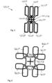
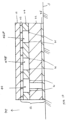
- Fig. 5 shows a module lead frame 43LF.
- the module lead frame 43LF includes a module lead frame body 43LFB, six module lead frame fingers 43LFF, and six module lead frame contact pads 43CP.
- the module lead frame body 43LFB is connected to the module lead frame fingers 43LFF.
- the module lead frame fingers 43LFF are connected to the corresponding module lead frame contact pads 43CP.
- Fig. 6 shows a sensor lead frame 46LF.
- the sensor lead frame 46LF includes a sensor lead frame body 46LFB, eight sensor lead frame fingers 46LFF, and eight sensor lead frame contact pads 46CP.
- the sensor lead frame body 46LFB is connected to the sensor lead frame fingers 46LFF.
- the sensor lead frame fingers 46LFF are connected to the corresponding sensor lead frame contact pads 46CP.
- the inlay 12 can include 4 or more layers.
- the inlay 12 can have 5 layers, an intermediate transparent PVC sheet being provided next to the second transparent overlay sheet 35.
- the card 10 can include 8 or more layers. In other words, the card can have 9 or 10 layers.
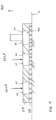
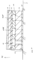
- the method includes a step of providing an antenna carrier sheet 29, as one of plurality of antenna carrier sheets in a large material sheet.
- the antenna carrier sheet 29 is punched to provide a first opening O1 for receiving the printed circuit board 40PCB of the secure processing module 40, a second opening O2 for receiving a module lead frame 43LF, and a third opening O3 for receiving a sensor lead frame 46LF. This is shown in Fig. 7 .
- An intermediary self-adhesive tape 28 is then placed on the first major surface 29S1 of the antenna carrier sheet 29 such that the self-adhesive tape 28 covers the antenna carrier sheet 29.
- the intermediary self-adhesive tape 28 and the antenna carrier sheet 29 are also placed such that a non-adhesive surface of the self-adhesive tape 28 is resting on a support surface S, while a self-adhesive surface of the self-adhesive tape 28 faces the first major surface 29S1. This is shown in Fig. 7 .
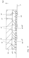
- a secure processing module 40 is later picked and placed into the first opening O1, wherein the printed circuit board 40PCB of the secure processing module 40 contacts the self-adhesive tape 28 and is attached to the adhesive layer of the self-adhesive tape 28.
- the adhesive layer acts to fix the printed circuit board 40PCB to the self-adhesive tape 28.
- the self-adhesive tape 28 prevents the printed circuit board 40PCB from falling off.
- the insertion is also done such that the electrical contact pads of the printed circuit board 40PCB lie in the plane of the first major surface 29S1 of the antenna carrier sheet 29, as illustrated in Fig. 8 .
- a module lead frame 43LF is inserted into the second opening O2, wherein the module lead frame 43LF contacts the self-adhesive tape 28 and is attached to the adhesive layer of the self-adhesive tape 28.
- the adhesive layer acts to fix the module lead frame 43LF to the self-adhesive tape 28.
- the insertion is also done such that an exposed surface of the module lead frame 43LF lie in the plane of the first major surface 29S1 of the antenna carrier sheet 29, as illustrated in Fig. 8 .
- a sensor lead frame 46LF is picked and is placed in the third opening O3. wherein the sensor lead frame 46LF contacts the self-adhesive tape 28 and is attached to the adhesive layer of the self-adhesive tape 28.
- the adhesive layer acts to fix the sensor lead frame 46LF to the self-adhesive tape 28.
- the insertion is done such that an exposed surface of the sensor lead frame 46LF lie in the plane of the first major surface 29S1 of the antenna carrier sheet 29, as illustrated in Fig. 8 .
- An antenna A comprises a coil of electrical conductor is also placed on and is embedded into the antenna carrier sheet 29. In other words, the antenna A is firmly attached to the antenna carrier sheet 29. A heated tool presses the antenna onto the antenna carrier sheet 29, which includes a thermoplastic material.
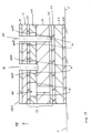
- the antenna A is shown in Fig. 22 , which shows a view of a top of the cash 10 of Fig. 1 when the layers 27, 29, 17, 15 are transparent.
- Electrical wires W are afterward electrically connected to the electrical contact pads of the printed circuit board 40PCB of the secure processing module 40, to the second ends 43CP2 of the module lead frame contact pads 43CP, and to the second ends 46CP2 of the sensor lead frame contact pads 46CP, as illustrated in Fig. 9 .
- the attachment of the electrical wires W is done using thermal compression bonding.
- the attachment of the electrical wires W is done using ultrasonic bonding.
- the ultrasonic bonding refers to rubbing together two pieces of metal with high energy such that surface impurities on surfaces of these two metals are scrubbed away and that underlying atoms of the metals are brought into close contact for bonding.
- the energy for this mechanically rubbing of the two metals is provided by a tool that vibrates mechanically at an ultrasonic frequency.
- the electrical wires W also electrically connects the electrical conductor of the antenna A to the electrical contact pads of the printed circuit board 40PCB of the secure processing module 40.
- the electrical wires W can overlap each other, as seen in Fig. 22 .
- a thickness compensation sheet 32 is provided as one of a plurality of compensation sheets in a large material sheet MS.
- the large material sheet MS is illustrated in Fig. 23 .
- the thickness compensation sheet 32 is punched to provide an opening to receive the moulded part 40MP of the secure processing module 40.
- the thickness compensation sheet 32 is later placed on the 29S2 of the antenna carrier sheet 29 such the thickness compensation sheet 32 covers the outer end of the antenna carrier sheet 29. The placing is also done such the opening of the thickness compensation sheet 32 receives the moulded part 40MP, as illustrated in Fig. 10 .
- the partial inlay 12 is then flipped or turned over, wherein the self-adhesive tape 28 is then removed and replaced by a first transparent overlay sheet 27 is provided as one of a plurality of transparent overlay sheets in a large material sheet.
- the partial inlay 12 is later flipped over again, wherein the first transparent overlay sheet 27 is resting and touching the support surface S, as seen Fig. 11 .
- a second transparent overlay sheet 35 is provided as one of a plurality of transparent overlay sheets in a large material sheet and it is placed on the thickness compensation sheet 32 such that the second transparent overlay sheet 35 covers the thickness compensation sheet 32, as illustrated in Fig. 11 .
- the first transparent overlay sheet 27, the antenna carrier sheet 29, the thickness compensation sheet 32, and the second transparent overlay sheet 35 are then laminated, wherein these sheets are pressed against each other to form the complete inlay 12.
- the electrical wires W allows flexible electrical connections between the secure processing module 40 and the module lead frame contact pads 43CP and between the secure processing module 40 and the sensor lead frame contact pads 46CP.
- the electrical connections can be configured easily by simply setting software parameters for defining required connections between parts. A user can then easily adapt its production process to use a different part with a different contact pad configuration. This is different from the printed circuit board that provides fixed electrical connections between parts.
- a method of producing a card using the inlay 12 is described below.
- the method includes a step of resting the inlay 12 on the support surface S, wherein the second transparent overlay sheet 35 is touching the support surface S, as illustrated in Fig. 12 .
- a first printed PVC sheet 17 as one of a plurality of printed PVC sheets in a large material sheet is then provided and it is placed on the first transparent overlay sheet 27 of the inlay 12, such that the first printed PVC sheet 17 covers the first transparent overlay sheet 27, as illustrated in Fig. 13 .
- a first transparent PVC sheet 15 is then provided as one of a plurality of transparent PVC sheets in a large material sheet and it is then placed on the first printed PVC sheet 17 such that the first transparent PVC sheet 15 covers the first printed PVC sheet 17, as illustrated in Fig. 14 .
- the partial card 10 is then flipped over such that the first transparent PVC sheet 15 is resting on and touching the support surface S, as illustrated in Fig. 15 .
- An intermediate transparent PVC sheet 20 is provided as one of a plurality of intermediate transparent PVC sheets in a large material sheet and it is afterward placed on the second transparent overlay sheet 35 of the inlay 12 such that the intermediate transparent PVC sheet 20 covers the second transparent overlay sheet 35, as illustrated in Fig. 16 .
- a second printed PVC sheet 23 is provided as one of a plurality of printed PVC sheets in a large material sheet and it is later placed on the intermediate transparent PVC sheet 20 such that the second printed PVC sheet 23 covers the intermediate transparent PVC sheet 20, as illustrated in Fig. 17 .
- the intermediate transparent PVC sheet 20 is left away.
- a second transparent PVC sheet 25 is provided as one of a plurality of transparent PVC sheets in a large material sheet and it is afterward placed on the second printed PVC sheet 23 such that the second transparent PVC sheet 25 covers the second printed PVC sheet 23, as illustrated in Fig. 18 .
- the second transparent PVC sheet 25 is placed on the support surface S, as illustrated in Fig. 19 .
- a sharp rotating tool is then applied perpendicularly to the first major surface 15S1 to cut or mill into the first major surface 15S1.
- the milling is done deep enough such that the module lead frame body 43LFB is cut such that it is electrically detached from the module lead frame contact pads 43CP.
- the milling creates a recess R1 that extends from the first major surface 15S1 to the module lead frame body 43LFB.
- This milling also creates a shallow hole in the thickness compensation sheet 32.
- the recess R1 extends from the first major surface 15S1 into a part of the thickness compensation sheet 32.
- the recess R1 is shown in Fig. 19 .
- the first major surface 15S1 is milled into the partial card 10 such that the sensor lead frame body 46LFB is cut such that it is electrically detached from the sensor lead frame contact pads 46CP.
- the milling creates a recess R2 that extends from the first major surface 15S1 to the sensor lead frame body 46LFB. This recess R2 is shown in Fig. 19 .
- This milling also creates a hole or recess R5 that goes through the thickness compensation sheet 32 and into the second transparent overlay sheet 35.
- the recess R5 extends from the thickness compensation sheet 32 and into the second transparent overlay sheet 35. This recess R5 is large enough to receive the second rectangular part 46P2 of the fingerprint sensor 46.
- the recess R5 is shown in Fig. 20 .
- the first major surface 15S1 is then milled again to create a bigger recess R3 that extends from the first major surface 15S1 to the module lead frame contact pads 43CP.
- This recess R3 is large enough to receive the contact module 43.
- the milling also exposes the module lead frame contact pads 43CP.
- the recess R3 is shown in Fig. 20 . Put differently, the milling eats into the module lead frame contact pads 43CP.
- the first major surface 15S1 is then milled again to create a bigger recess R4 that extends the first major surface 15S1 to the sensor lead frame contact pads 46CP.
- This recess is large enough to receive the first rectangular part 46P1 of the fingerprint sensor 46.
- the milling also exposes the sensor lead frame contact pads 46CP.
- the recess R4 is shown in Fig. 20 . The milling eats into the sensor lead frame contact pads 46CP.
- the milling steps can also be applied in a reversed order or other sequence.
- the milling step to electrically detach the module lead frame body 43LFB from the module lead frame contact pads 43CP can be done before or after the step of milling to create recess R3.
- the milling step to electrically detach the sensor lead frame body 46LFB from the sensor lead frame contact pads 46CP can be done before or after the step of milling to create the recess R4.
- An electrically conductive substance is later placed either on the inner module contact pads of the contact module 43 or on the exposed module lead frame contact pads 43CP.
- the contact module 43 is later inserted in the respective recess such that the inner module contact pads of the contact module 43 are electrically connected to the module lead frame contact pads 43CP via the electrically conductive substance.
- an electrically conductive substance is later placed either on the inner sensor contact pads of the fingerprint sensor 46 or on the exposed sensor lead frame contact pads 46CP.
- the fingerprint sensor 46 is then inserted in the respective recess such that the inner sensor contact pads of the fingerprint sensor 46 are electrically connected to the sensor lead frame contact pads 46CP via the electrically conductive substance to form the complete card 10, as illustrated in Fig. 1 .
Landscapes
- Engineering & Computer Science (AREA)
- Computer Hardware Design (AREA)
- Theoretical Computer Science (AREA)
- Physics & Mathematics (AREA)
- General Physics & Mathematics (AREA)
- Microelectronics & Electronic Packaging (AREA)
- Manufacturing & Machinery (AREA)
- Computer Networks & Wireless Communication (AREA)
- Computer Security & Cryptography (AREA)
- General Engineering & Computer Science (AREA)
- Multimedia (AREA)
- Human Computer Interaction (AREA)
- Automation & Control Theory (AREA)
- Credit Cards Or The Like (AREA)
- Image Input (AREA)
Claims (14)
- Einlage (12) für eine Karte (10), wobei die Einlage (12) Folgendes aufweist:eine erste transparente Deckschicht (27),eine Antennenträgerschicht (29), die neben der ersten transparenten Deckschicht (27) vorgesehen ist, wobei die Antennenträgerschicht (29) eine Mikrocontrolleröffnung (O1), eine Kontaktmodul-Leiterrahmenöffnung (O2) und eine Fingersensor-Leiterrahmenöffnung (O3) aufweist,eine Dickenausgleichsschicht (32), die neben der Antennenträgerschicht (29) vorgesehen ist,eine zweite transparente Deckschicht (35), die neben der Dickenausgleichsschicht (32) vorgesehen ist,einen Mikrocontroller (40), der in der Mikrocontrolleröffnung (O1) vorgesehen ist,einen Modul-Leiterrahmen (43LF), der ausgebildet ist, gefräst zu werden, und in der Kontaktmodul-Leiterrahmenöffnung (O2) vorgesehen ist, wobei der Modul-Leiterrahmen (43LFB) eine Mehrzahl von ersten Kontaktflächen (43CP) zum Kontaktieren eines Kontaktmoduls (43) aufweist,einen Fingersensor-Leiterrahmen (46LF), der ausgebildet ist, gefräst zu werden und in der Fingersensor-Leiterrahmenöffnung (O3) vorgesehen ist, wobei der Fingersensor-Leiterrahmen (46LF) eine Mehrzahl von zweiten Kontaktflächen (46CP) zum Kontaktieren eines Fingerabdrucksensors (46) aufweist,eine Antenne (A) aufweisend eine Spule aus einem Leiter, die in die Antennenträgerschicht (29) eingebettet ist, undeine Mehrzahl von elektrischen Drähten (W), die mit dem Mikrocontroller (40), mit den ersten Kontaktflächen (43CP), mit den zweiten Kontaktflächen (46CP) und mit der Antenne (A) verbunden sind.
- Einlage (12) nach Anspruch 1, wobei
mindestens ein elektrischer Draht mit einem anderen elektrischen Draht überlappt. - Einlage (12) nach Anspruch 1, zudem aufweisend
eine transparente PVC-Zwischenschicht (20), die neben der zweiten transparenten Deckschicht (35) vorgesehen ist. - Verfahren zum Herstellen einer Einlage, wobei das Verfahren Folgendes aufweist:Vorsehen einer Antennenträgerschicht (29),Vorsehen der Antennenträgerschicht (29) mit einer ersten Öffnung (O1) zur Aufnahme einer Leiterplatte (40PCB) eines Mikrocontrollers (40), einer zweiten Öffnung (O2) zur Aufnahme eines Modul-Leiterrahmens (43LF) und einer dritten Öffnung (O3) zur Aufnahme eines Sensor-Leiterrahmens (46LF),Vorsehen eines Klebebandes (28) neben der Antennenträgerschicht (29),Einsetzen der Leiterplatte (40PCB) in die erste Öffnung (O1), Einsetzen des Modul-Leiterrahmens (43LF) in die zweite Öffnung (O2), Einsetzen des Sensor-Leiterrahmens (46LF) in die dritte Öffnung (O3), wobei die Leiterplatte (40PCB), der Modul-Leiterrahmens (43LF) und der Sensor-Leiterrahmen (46LF) an dem Klebeband (28) befestigt werden,Einbetten einer Antenne (A) aufweisend eine Spule aus einem Leiter in die Antennenträgerschicht (29),Befestigen einer Mehrzahl von elektrischen Drähten (W) an elektrischen Kontaktflächen der Leiterplatte (40PCB), an dem Modul-Leiterrahmen (43LF), an dem Sensor-Leiterrahmen (46LF) und an der Antenne (A),Vorsehen einer Dickenausgleichsschicht (32) mit einer Öffnung zur Aufnahme eines Formteils (40MP) des Mikrocontrollers (40),Vorsehen der Dickenausgleichsschicht (32) neben der Antennenträgerschicht (29),Entfernen des Klebebandes (28) von der Antennenträgerschicht (29),Vorsehen einer ersten transparenten Deckschicht (27) neben der Antennenträgerschicht (29), undVorsehen einer zweiten transparenten Deckschicht (35) neben der Dickenausgleichsschicht (32).
- Verfahren nach Anspruch 4 zudem aufweisend
Vorsehen einer transparente PVC-Zwischenschicht (20) neben der zweiten transparenten Deckschicht (35). - Karte (10), aufweisend
eine Einlage (12) nach Anspruch 1,
wobei die Karte weiterhin Folgendes aufweist:eine erste bedruckte PVC-Schicht (17), die neben einer ersten transparenten Deckschicht (27) der Einlage (12) vorgesehen ist,eine erste transparente PVC-Schicht (15), die neben der ersten bedruckten PVC-Schicht (17) vorgesehen ist,eine zweite bedruckte PVC-Schicht (23), die neben einer zweiten transparenten Deckschicht (35) der Einlage (12) vorgesehen ist,eine zweite bedruckte PVC-Schicht (23), die neben der transparenten PVC-Zwischenschicht (20) vorgesehen ist,eine zweite transparente PVC-Schicht (25), die neben der zweiten bedruckten PVC-Schicht (23) vorgesehen ist, wobei die erste transparente PVC-Schicht (15), die erste bedruckte PVC-Schicht (17) und die erste transparente Deckschicht (27) eine Kontaktmodulöffnung und eine Fingerabdrucksensoröffnung aufweisen,ein Kontaktmodul (43), das in der Kontaktmodulöffnung vorgesehen ist und elektrisch mit den ersten Kontaktflächen (43CP) verbunden ist, undeinen Fingerabdrucksensor (46), der in der Fingerabdrucksensoröffnung vorgesehen ist und elektrisch mit den zweiten Kontaktflächen (46CP) verbunden ist. - Karte nach Anspruch 6, weiterhin aufweisend
eine transparente PVC-Zwischenschicht (20), die zwischen der zweiten transparenten Deckschicht (35) und der zweiten bedruckten PVC-Schicht (23) vorgesehen ist. - Karte nach Anspruch 6, wobei
mindestens ein elektrischer Draht mit einem anderen elektrischen Draht überlappt. - Karte nach Anspruch 6, weiterhin aufweisend
eine erste elektrisch leitende Substanz zur elektrischen Verbindung des Kontaktmoduls (43) mit den ersten Kontaktflächen (43CP). - Karte nach Anspruch 6, weiterhin aufweisend
eine zweite elektrisch leitende Substanz zur elektrischen Verbindung des Fingerabdrucksensors (46) mit den zweiten Kontaktflächen (46CP). - Verfahren zum Herstellen einer Karte, wobei das Verfahren aufweist:Vorsehen einer Einlage nach dem Verfahren zum Herstellen einer Einlage nach Anspruch 4,Vorsehen einer ersten bedruckten PVC-Schicht (17) neben einer ersten transparenten Deckschicht (27) der Einlage (12),Vorsehen einer ersten transparenten PVC-Schicht (15) neben der ersten transparenten PVC-Schicht (15),Vorsehen einer zweiten bedruckten PVC-Schicht (23) neben einer zweiten transparenten Deckschicht (35) der Einlage (12),Vorsehen einer zweiten transparenten PVC-Schicht (25) neben der zweiten bedruckten PVC-Schicht (23),Fräsen einer ersten Hauptoberfläche (15S1) der ersten transparenten PVC-Schicht (15), so dass ein Modul-Leiterrahmenkörper (43LFB) eines Modul-Leiterrahmens (43LF) elektrisch von Modul-Leiterrahmen-Kontaktflächen (43CP) des Modul-Leiterrahmens (43LF) getrennt wird,Fräsen der ersten Hauptoberfläche (15S1), so dass ein Sensor-Leiterrahmenkörper (46LFB) eines Sensor-Leiterrahmens (46LF) elektrisch von Sensor-Leiterrahmen-Kontaktflächen (46CP) des Sensor-Leiterrahmens (46LF) getrennt wird,Fräsen der ersten Hauptfläche (15S1), um eine erste Ausnehmung zur Aufnahme eines Kontaktmoduls (43) vorzusehen, undFräsen der ersten Hauptfläche (15S1), um eine zweite Ausnehmung zur Aufnahme eines Fingerabdrucksensors (46) vorzusehen.
- Verfahren nach Anspruch 11, weiterhin aufweisendEinsetzen eines Kontaktmoduls (43) in die erste Ausnehmung, wobei das Kontaktmodul (43) elektrisch mit den Modul-Leiterrahmen-Kontaktflächen (43CP) verbunden wird, undEinsetzen eines Fingerabdrucksensors (46) in die zweite Ausnehmung, wobei der Fingerabdrucksensor (46) elektrisch mit den Sensor-Leiterrahmen-Kontaktflächen (46CP) verbunden wird.
- Verfahren nach Anspruch 11, weiterhin aufweisend
Vorsehen einer ersten elektrisch leitenden Substanz zur elektrischen Verbindung des Kontaktmoduls (43) mit den Modul-Leiterrahmen-Kontaktflächen (43CP). - Verfahren nach Anspruch 11, weiterhin aufweisend
Vorsehen einer zweiten elektrisch leitenden Substanz zur elektrischen Verbindung des Fingerabdrucksensors (46) mit den Sensor-Leiterrahmen-Kontaktflächen (46CP).
Applications Claiming Priority (2)
| Application Number | Priority Date | Filing Date | Title |
|---|---|---|---|
| SG10201902933WA SG10201902933WA (en) | 2019-04-01 | 2019-04-01 | An improved card with fingerprint biometrics |
| PCT/SG2020/050199 WO2020204831A1 (en) | 2019-04-01 | 2020-04-01 | An improved card with fingerprint biometrics |
Publications (3)
| Publication Number | Publication Date |
|---|---|
| EP3948667A1 EP3948667A1 (de) | 2022-02-09 |
| EP3948667A4 EP3948667A4 (de) | 2022-12-21 |
| EP3948667B1 true EP3948667B1 (de) | 2024-10-30 |
Family
ID=72667488
Family Applications (1)
| Application Number | Title | Priority Date | Filing Date |
|---|---|---|---|
| EP20784246.9A Active EP3948667B1 (de) | 2019-04-01 | 2020-04-01 | Verbesserte karte mit fingerabdruckbiometriken |
Country Status (6)
| Country | Link |
|---|---|
| US (2) | US11769029B2 (de) |
| EP (1) | EP3948667B1 (de) |
| CN (1) | CN113632103A (de) |
| HU (1) | HUE069949T2 (de) |
| SG (1) | SG10201902933WA (de) |
| WO (2) | WO2020204815A2 (de) |
Families Citing this family (4)
| Publication number | Priority date | Publication date | Assignee | Title |
|---|---|---|---|---|
| CN116997905A (zh) * | 2021-03-23 | 2023-11-03 | 指纹卡安娜卡敦知识产权有限公司 | 指纹传感器模块和用于制造指纹传感器模块的方法 |
| US12217114B2 (en) | 2021-07-15 | 2025-02-04 | Linxens Holding | Lead-frame, card body of a smart card, smart card, and method of forming a smart card |
| WO2023095918A1 (ja) * | 2021-11-29 | 2023-06-01 | 凸版印刷株式会社 | インレット及びカード型媒体 |
| CN116933830A (zh) | 2022-04-06 | 2023-10-24 | 群创光电股份有限公司 | 卡片装置及制造卡片装置的方法 |
Family Cites Families (18)
| Publication number | Priority date | Publication date | Assignee | Title |
|---|---|---|---|---|
| US7070112B2 (en) * | 1999-09-07 | 2006-07-04 | American Express Travel Related Services Company, Inc. | Transparent transaction device |
| PA8581901A1 (es) * | 2002-09-10 | 2004-05-21 | Ivi Smart Technologies Inc | Verificacion biometrica segura de identidad |
| WO2006101493A1 (en) | 2005-03-23 | 2006-09-28 | Cardxx, Inc. | Method for making advanced smart cards with integrated electronics using isotropic thermoset adhesive materials with high quality exterior surfaces |
| US7599192B2 (en) * | 2005-04-11 | 2009-10-06 | Aveso, Inc. | Layered structure with printed elements |
| EP2013821B1 (de) | 2006-04-10 | 2011-10-12 | Innovatier, Inc. | Elektronisches einlagemodul für elektronikkarten und etiketten, elektronikkarte und verfahren zur herstellung derartiger elektronischer einlagemodule und karten |
| US8322624B2 (en) * | 2007-04-10 | 2012-12-04 | Feinics Amatech Teoranta | Smart card with switchable matching antenna |
| KR20100114133A (ko) * | 2008-03-18 | 2010-10-22 | 픽셀옵틱스, 인크. | 진보한 전기-활성 광학 장치 |
| US8823497B2 (en) * | 2012-02-14 | 2014-09-02 | International Business Machines Corporation | Secure data card with passive RFID chip and biometric sensor |
| EP3035173B1 (de) * | 2014-12-15 | 2018-02-07 | Nxp B.V. | Benutzerschnittstelleneinheit, elektronische Vorrichtung und Herstellungsverfahren |
| US9792516B2 (en) * | 2016-01-26 | 2017-10-17 | Next Biometrics Group Asa | Flexible card with fingerprint sensor |
| GB2548639A (en) | 2016-03-24 | 2017-09-27 | Zwipe As | Method of manufacturing a smartcard |
| KR101706592B1 (ko) | 2016-09-21 | 2017-02-15 | 유비씨엔(주) | 보안기능이 강화된 지문인식 rf 스마트카드 및 그 제어방법 |
| US10395164B2 (en) * | 2016-12-15 | 2019-08-27 | Fingerprint Cards Ab | Fingerprint sensing module and method for manufacturing the fingerprint sensing module |
| FR3063555B1 (fr) * | 2017-03-03 | 2021-07-09 | Linxens Holding | Carte a puce et procede de fabrication d’une carte a puce |
| SE1750836A1 (en) * | 2017-06-28 | 2018-12-29 | Fingerprint Cards Ab | Fingerprint sensor module comprising antenna and method for manufacturing a fingerprint sensor module |
| FR3069081B1 (fr) | 2017-07-17 | 2021-08-20 | Safran Identity & Security | Carte electronique comprenant un capteur d'empreinte et procede de fabrication d'une telle carte |
| CN207397314U (zh) * | 2017-08-25 | 2018-05-22 | 苏晓虎 | 一种带有指纹识别模块的电子卡片 |
| GB2584434A (en) * | 2019-05-31 | 2020-12-09 | Advanide Holdings Pte Ltd | Enrolment device for a biometric smart card |
-
2019
- 2019-04-01 SG SG10201902933WA patent/SG10201902933WA/en unknown
-
2020
- 2020-03-25 WO PCT/SG2020/050160 patent/WO2020204815A2/en not_active Ceased
- 2020-04-01 US US17/598,326 patent/US11769029B2/en active Active
- 2020-04-01 EP EP20784246.9A patent/EP3948667B1/de active Active
- 2020-04-01 CN CN202080024495.5A patent/CN113632103A/zh active Pending
- 2020-04-01 HU HUE20784246A patent/HUE069949T2/hu unknown
- 2020-04-01 WO PCT/SG2020/050199 patent/WO2020204831A1/en not_active Ceased
-
2023
- 2023-09-19 US US18/370,200 patent/US20240013021A1/en not_active Abandoned
Also Published As
| Publication number | Publication date |
|---|---|
| US20220180142A1 (en) | 2022-06-09 |
| CN113632103A (zh) | 2021-11-09 |
| HUE069949T2 (hu) | 2025-04-28 |
| WO2020204831A1 (en) | 2020-10-08 |
| SG10201902933WA (en) | 2020-11-27 |
| EP3948667A1 (de) | 2022-02-09 |
| EP3948667A4 (de) | 2022-12-21 |
| US11769029B2 (en) | 2023-09-26 |
| US20240013021A1 (en) | 2024-01-11 |
| WO2020204815A2 (en) | 2020-10-08 |
Similar Documents
| Publication | Publication Date | Title |
|---|---|---|
| EP3948667B1 (de) | Verbesserte karte mit fingerabdruckbiometriken | |
| EP3159832B1 (de) | Authentifizierungstoken | |
| US8172978B2 (en) | Reinforced radio frequency identification device support and its manufacturing method | |
| CN104380313B (zh) | 制造电子卡的方法 | |
| CN109271835B (zh) | 具有指纹采集器的电子板及其制造方法 | |
| CN108780516B (zh) | 制造智能卡的方法 | |
| US20050139685A1 (en) | Design & method for manufacturing low-cost smartcards with embedded fingerprint authentication system modules | |
| CN114341876A (zh) | 生物识别智能卡的登记装置 | |
| CN105512715B (zh) | 芯片卡模块装置、芯片卡装置和用于制造芯片卡装置的方法 | |
| TW200414064A (en) | Subscriber identification module, subscriber identification module holder, IC module, IC card and IC card holder | |
| CN103119616A (zh) | 聚碳酸酯制射频识别设备及其制造方法 | |
| CN114600123A (zh) | 具有生物识别特征的金属卡 | |
| US10268942B2 (en) | Packaged electronic module and manufacturing method thereof | |
| CN105378760A (zh) | Ic模块、双ic卡、以及ic模块的制造方法 | |
| CN115552410B (zh) | 卡式介质 | |
| CN101243457B (zh) | 包含数据传送步骤的电子产品的制作方法及所制得的成品 | |
| CN116529734A (zh) | 卡型介质以及卡型介质的制造方法 | |
| KR101249137B1 (ko) | 콤비카드 제조방법 | |
| WO2022243432A1 (en) | Manufacturing a smartcard | |
| KR20080084767A (ko) | 전자카드 모듈 및 그 제조방법 | |
| KR102856550B1 (ko) | 전자 카드 제조 방법 | |
| JP4085790B2 (ja) | Icカードの製造方法 | |
| WO2025083441A1 (en) | Sensor module | |
| TW202248903A (zh) | 製造智慧卡 | |
| JP2024041553A (ja) | Icカード、icカードの処理方法、カード処理システム、ic交換セット |
Legal Events
| Date | Code | Title | Description |
|---|---|---|---|
| STAA | Information on the status of an ep patent application or granted ep patent |
Free format text: STATUS: THE INTERNATIONAL PUBLICATION HAS BEEN MADE |
|
| PUAI | Public reference made under article 153(3) epc to a published international application that has entered the european phase |
Free format text: ORIGINAL CODE: 0009012 |
|
| STAA | Information on the status of an ep patent application or granted ep patent |
Free format text: STATUS: REQUEST FOR EXAMINATION WAS MADE |
|
| 17P | Request for examination filed |
Effective date: 20210924 |
|
| AK | Designated contracting states |
Kind code of ref document: A1 Designated state(s): AL AT BE BG CH CY CZ DE DK EE ES FI FR GB GR HR HU IE IS IT LI LT LU LV MC MK MT NL NO PL PT RO RS SE SI SK SM TR |
|
| DAV | Request for validation of the european patent (deleted) | ||
| DAX | Request for extension of the european patent (deleted) | ||
| REG | Reference to a national code |
Ref country code: DE Ref legal event code: R079 Free format text: PREVIOUS MAIN CLASS: G06K0019073000 Ipc: G06K0019070000 Ref country code: DE Ref legal event code: R079 Ref document number: 602020040396 Country of ref document: DE Free format text: PREVIOUS MAIN CLASS: G06K0019073000 Ipc: G06K0019070000 |
|
| A4 | Supplementary search report drawn up and despatched |
Effective date: 20221121 |
|
| RIC1 | Information provided on ipc code assigned before grant |
Ipc: G06V 40/13 20220101ALI20221115BHEP Ipc: B42D 25/46 20140101ALI20221115BHEP Ipc: B42D 25/455 20140101ALI20221115BHEP Ipc: B42D 25/305 20140101ALI20221115BHEP Ipc: B42D 25/23 20140101ALI20221115BHEP Ipc: G06K 19/07 20060101AFI20221115BHEP |
|
| GRAP | Despatch of communication of intention to grant a patent |
Free format text: ORIGINAL CODE: EPIDOSNIGR1 |
|
| STAA | Information on the status of an ep patent application or granted ep patent |
Free format text: STATUS: GRANT OF PATENT IS INTENDED |
|
| INTG | Intention to grant announced |
Effective date: 20240521 |
|
| GRAS | Grant fee paid |
Free format text: ORIGINAL CODE: EPIDOSNIGR3 |
|
| GRAA | (expected) grant |
Free format text: ORIGINAL CODE: 0009210 |
|
| STAA | Information on the status of an ep patent application or granted ep patent |
Free format text: STATUS: THE PATENT HAS BEEN GRANTED |
|
| AK | Designated contracting states |
Kind code of ref document: B1 Designated state(s): AL AT BE BG CH CY CZ DE DK EE ES FI FR GB GR HR HU IE IS IT LI LT LU LV MC MK MT NL NO PL PT RO RS SE SI SK SM TR |
|
| REG | Reference to a national code |
Ref country code: GB Ref legal event code: FG4D |
|
| REG | Reference to a national code |
Ref country code: CH Ref legal event code: EP |
|
| REG | Reference to a national code |
Ref country code: IE Ref legal event code: FG4D |
|
| REG | Reference to a national code |
Ref country code: DE Ref legal event code: R096 Ref document number: 602020040396 Country of ref document: DE |
|
| P01 | Opt-out of the competence of the unified patent court (upc) registered |
Free format text: CASE NUMBER: APP_65833/2024 Effective date: 20241213 |
|
| REG | Reference to a national code |
Ref country code: LT Ref legal event code: MG9D |
|
| REG | Reference to a national code |
Ref country code: NL Ref legal event code: MP Effective date: 20241030 |
|
| PG25 | Lapsed in a contracting state [announced via postgrant information from national office to epo] |
Ref country code: IS Free format text: LAPSE BECAUSE OF FAILURE TO SUBMIT A TRANSLATION OF THE DESCRIPTION OR TO PAY THE FEE WITHIN THE PRESCRIBED TIME-LIMIT Effective date: 20250228 Ref country code: PT Free format text: LAPSE BECAUSE OF FAILURE TO SUBMIT A TRANSLATION OF THE DESCRIPTION OR TO PAY THE FEE WITHIN THE PRESCRIBED TIME-LIMIT Effective date: 20250228 Ref country code: HR Free format text: LAPSE BECAUSE OF FAILURE TO SUBMIT A TRANSLATION OF THE DESCRIPTION OR TO PAY THE FEE WITHIN THE PRESCRIBED TIME-LIMIT Effective date: 20241030 |
|
| PG25 | Lapsed in a contracting state [announced via postgrant information from national office to epo] |
Ref country code: FI Free format text: LAPSE BECAUSE OF FAILURE TO SUBMIT A TRANSLATION OF THE DESCRIPTION OR TO PAY THE FEE WITHIN THE PRESCRIBED TIME-LIMIT Effective date: 20241030 Ref country code: NL Free format text: LAPSE BECAUSE OF FAILURE TO SUBMIT A TRANSLATION OF THE DESCRIPTION OR TO PAY THE FEE WITHIN THE PRESCRIBED TIME-LIMIT Effective date: 20241030 |
|
| PGFP | Annual fee paid to national office [announced via postgrant information from national office to epo] |
Ref country code: BG Payment date: 20250310 Year of fee payment: 6 |
|
| PG25 | Lapsed in a contracting state [announced via postgrant information from national office to epo] |
Ref country code: ES Free format text: LAPSE BECAUSE OF FAILURE TO SUBMIT A TRANSLATION OF THE DESCRIPTION OR TO PAY THE FEE WITHIN THE PRESCRIBED TIME-LIMIT Effective date: 20241030 |
|
| PG25 | Lapsed in a contracting state [announced via postgrant information from national office to epo] |
Ref country code: NO Free format text: LAPSE BECAUSE OF FAILURE TO SUBMIT A TRANSLATION OF THE DESCRIPTION OR TO PAY THE FEE WITHIN THE PRESCRIBED TIME-LIMIT Effective date: 20250130 |
|
| PG25 | Lapsed in a contracting state [announced via postgrant information from national office to epo] |
Ref country code: GR Free format text: LAPSE BECAUSE OF FAILURE TO SUBMIT A TRANSLATION OF THE DESCRIPTION OR TO PAY THE FEE WITHIN THE PRESCRIBED TIME-LIMIT Effective date: 20250131 Ref country code: LV Free format text: LAPSE BECAUSE OF FAILURE TO SUBMIT A TRANSLATION OF THE DESCRIPTION OR TO PAY THE FEE WITHIN THE PRESCRIBED TIME-LIMIT Effective date: 20241030 |
|
| PG25 | Lapsed in a contracting state [announced via postgrant information from national office to epo] |
Ref country code: PL Free format text: LAPSE BECAUSE OF FAILURE TO SUBMIT A TRANSLATION OF THE DESCRIPTION OR TO PAY THE FEE WITHIN THE PRESCRIBED TIME-LIMIT Effective date: 20241030 |
|
| REG | Reference to a national code |
Ref country code: HU Ref legal event code: AG4A Ref document number: E069949 Country of ref document: HU |
|
| PG25 | Lapsed in a contracting state [announced via postgrant information from national office to epo] |
Ref country code: RS Free format text: LAPSE BECAUSE OF FAILURE TO SUBMIT A TRANSLATION OF THE DESCRIPTION OR TO PAY THE FEE WITHIN THE PRESCRIBED TIME-LIMIT Effective date: 20250130 |
|
| PG25 | Lapsed in a contracting state [announced via postgrant information from national office to epo] |
Ref country code: SM Free format text: LAPSE BECAUSE OF FAILURE TO SUBMIT A TRANSLATION OF THE DESCRIPTION OR TO PAY THE FEE WITHIN THE PRESCRIBED TIME-LIMIT Effective date: 20241030 |
|
| PGFP | Annual fee paid to national office [announced via postgrant information from national office to epo] |
Ref country code: DE Payment date: 20250202 Year of fee payment: 6 |
|
| PG25 | Lapsed in a contracting state [announced via postgrant information from national office to epo] |
Ref country code: DK Free format text: LAPSE BECAUSE OF FAILURE TO SUBMIT A TRANSLATION OF THE DESCRIPTION OR TO PAY THE FEE WITHIN THE PRESCRIBED TIME-LIMIT Effective date: 20241030 |
|
| PGFP | Annual fee paid to national office [announced via postgrant information from national office to epo] |
Ref country code: HU Payment date: 20250325 Year of fee payment: 6 |
|
| PG25 | Lapsed in a contracting state [announced via postgrant information from national office to epo] |
Ref country code: EE Free format text: LAPSE BECAUSE OF FAILURE TO SUBMIT A TRANSLATION OF THE DESCRIPTION OR TO PAY THE FEE WITHIN THE PRESCRIBED TIME-LIMIT Effective date: 20241030 |
|
| PGFP | Annual fee paid to national office [announced via postgrant information from national office to epo] |
Ref country code: FR Payment date: 20250425 Year of fee payment: 6 |
|
| PG25 | Lapsed in a contracting state [announced via postgrant information from national office to epo] |
Ref country code: RO Free format text: LAPSE BECAUSE OF FAILURE TO SUBMIT A TRANSLATION OF THE DESCRIPTION OR TO PAY THE FEE WITHIN THE PRESCRIBED TIME-LIMIT Effective date: 20241030 |
|
| PGFP | Annual fee paid to national office [announced via postgrant information from national office to epo] |
Ref country code: AT Payment date: 20250423 Year of fee payment: 6 |
|
| PG25 | Lapsed in a contracting state [announced via postgrant information from national office to epo] |
Ref country code: SK Free format text: LAPSE BECAUSE OF FAILURE TO SUBMIT A TRANSLATION OF THE DESCRIPTION OR TO PAY THE FEE WITHIN THE PRESCRIBED TIME-LIMIT Effective date: 20241030 |
|
| PG25 | Lapsed in a contracting state [announced via postgrant information from national office to epo] |
Ref country code: CZ Free format text: LAPSE BECAUSE OF FAILURE TO SUBMIT A TRANSLATION OF THE DESCRIPTION OR TO PAY THE FEE WITHIN THE PRESCRIBED TIME-LIMIT Effective date: 20241030 |
|
| PG25 | Lapsed in a contracting state [announced via postgrant information from national office to epo] |
Ref country code: IT Free format text: LAPSE BECAUSE OF FAILURE TO SUBMIT A TRANSLATION OF THE DESCRIPTION OR TO PAY THE FEE WITHIN THE PRESCRIBED TIME-LIMIT Effective date: 20241030 |
|
| REG | Reference to a national code |
Ref country code: DE Ref legal event code: R097 Ref document number: 602020040396 Country of ref document: DE |
|
| PLBE | No opposition filed within time limit |
Free format text: ORIGINAL CODE: 0009261 |
|
| STAA | Information on the status of an ep patent application or granted ep patent |
Free format text: STATUS: NO OPPOSITION FILED WITHIN TIME LIMIT |
|
| PG25 | Lapsed in a contracting state [announced via postgrant information from national office to epo] |
Ref country code: SE Free format text: LAPSE BECAUSE OF FAILURE TO SUBMIT A TRANSLATION OF THE DESCRIPTION OR TO PAY THE FEE WITHIN THE PRESCRIBED TIME-LIMIT Effective date: 20241030 |
|
| 26N | No opposition filed |
Effective date: 20250731 |
|
| REG | Reference to a national code |
Ref country code: CH Ref legal event code: H13 Free format text: ST27 STATUS EVENT CODE: U-0-0-H10-H13 (AS PROVIDED BY THE NATIONAL OFFICE) Effective date: 20251125 |
|
| PG25 | Lapsed in a contracting state [announced via postgrant information from national office to epo] |
Ref country code: LU Free format text: LAPSE BECAUSE OF NON-PAYMENT OF DUE FEES Effective date: 20250401 |
|
| PG25 | Lapsed in a contracting state [announced via postgrant information from national office to epo] |
Ref country code: MC Free format text: LAPSE BECAUSE OF FAILURE TO SUBMIT A TRANSLATION OF THE DESCRIPTION OR TO PAY THE FEE WITHIN THE PRESCRIBED TIME-LIMIT Effective date: 20241030 |
|
| REG | Reference to a national code |
Ref country code: BE Ref legal event code: MM Effective date: 20250430 |
|
| PG25 | Lapsed in a contracting state [announced via postgrant information from national office to epo] |
Ref country code: BE Free format text: LAPSE BECAUSE OF NON-PAYMENT OF DUE FEES Effective date: 20250430 |
|
| PG25 | Lapsed in a contracting state [announced via postgrant information from national office to epo] |
Ref country code: CH Free format text: LAPSE BECAUSE OF NON-PAYMENT OF DUE FEES Effective date: 20250430 |
|
| PGFP | Annual fee paid to national office [announced via postgrant information from national office to epo] |
Ref country code: GB Payment date: 20260204 Year of fee payment: 7 |
|
| PG25 | Lapsed in a contracting state [announced via postgrant information from national office to epo] |
Ref country code: IE Free format text: LAPSE BECAUSE OF NON-PAYMENT OF DUE FEES Effective date: 20250401 |
|
| PGFP | Annual fee paid to national office [announced via postgrant information from national office to epo] |
Ref country code: TR Payment date: 20260327 Year of fee payment: 7 |