EP3951006A1 - Matière première permettant la formation d'un film mince, procédé de production d'un film mince et composé de scandium - Google Patents
Matière première permettant la formation d'un film mince, procédé de production d'un film mince et composé de scandium Download PDFInfo
- Publication number
- EP3951006A1 EP3951006A1 EP20784999.3A EP20784999A EP3951006A1 EP 3951006 A1 EP3951006 A1 EP 3951006A1 EP 20784999 A EP20784999 A EP 20784999A EP 3951006 A1 EP3951006 A1 EP 3951006A1
- Authority
- EP
- European Patent Office
- Prior art keywords
- thin
- film
- raw material
- compound
- scandium
- Prior art date
- Legal status (The legal status is an assumption and is not a legal conclusion. Google has not performed a legal analysis and makes no representation as to the accuracy of the status listed.)
- Pending
Links
Images

Classifications
-
- C—CHEMISTRY; METALLURGY
- C23—COATING METALLIC MATERIAL; COATING MATERIAL WITH METALLIC MATERIAL; CHEMICAL SURFACE TREATMENT; DIFFUSION TREATMENT OF METALLIC MATERIAL; COATING BY VACUUM EVAPORATION, BY SPUTTERING, BY ION IMPLANTATION OR BY CHEMICAL VAPOUR DEPOSITION, IN GENERAL; INHIBITING CORROSION OF METALLIC MATERIAL OR INCRUSTATION IN GENERAL
- C23C—COATING METALLIC MATERIAL; COATING MATERIAL WITH METALLIC MATERIAL; SURFACE TREATMENT OF METALLIC MATERIAL BY DIFFUSION INTO THE SURFACE, BY CHEMICAL CONVERSION OR SUBSTITUTION; COATING BY VACUUM EVAPORATION, BY SPUTTERING, BY ION IMPLANTATION OR BY CHEMICAL VAPOUR DEPOSITION, IN GENERAL
- C23C16/00—Chemical coating by decomposition of gaseous compounds, without leaving reaction products of surface material in the coating, i.e. chemical vapour deposition [CVD] processes
- C23C16/06—Chemical coating by decomposition of gaseous compounds, without leaving reaction products of surface material in the coating, i.e. chemical vapour deposition [CVD] processes characterised by the deposition of metallic material
- C23C16/18—Chemical coating by decomposition of gaseous compounds, without leaving reaction products of surface material in the coating, i.e. chemical vapour deposition [CVD] processes characterised by the deposition of metallic material from metallo-organic compounds
-
- H—ELECTRICITY
- H10—SEMICONDUCTOR DEVICES; ELECTRIC SOLID-STATE DEVICES NOT OTHERWISE PROVIDED FOR
- H10P—GENERIC PROCESSES OR APPARATUS FOR THE MANUFACTURE OR TREATMENT OF DEVICES COVERED BY CLASS H10
- H10P14/00—Formation of materials, e.g. in the shape of layers or pillars
- H10P14/60—Formation of materials, e.g. in the shape of layers or pillars of insulating materials
- H10P14/69—Inorganic materials
- H10P14/692—Inorganic materials composed of oxides, glassy oxides or oxide-based glasses
- H10P14/6938—Inorganic materials composed of oxides, glassy oxides or oxide-based glasses the material containing at least one metal element, e.g. metal oxides, metal oxynitrides or metal oxycarbides
- H10P14/6939—Inorganic materials composed of oxides, glassy oxides or oxide-based glasses the material containing at least one metal element, e.g. metal oxides, metal oxynitrides or metal oxycarbides characterised by the metal
- H10P14/69396—Inorganic materials composed of oxides, glassy oxides or oxide-based glasses the material containing at least one metal element, e.g. metal oxides, metal oxynitrides or metal oxycarbides characterised by the metal the material containing at least one rare earth metal element, e.g. oxides of lanthanides, scandium or yttrium
-
- C—CHEMISTRY; METALLURGY
- C07—ORGANIC CHEMISTRY
- C07C—ACYCLIC OR CARBOCYCLIC COMPOUNDS
- C07C45/00—Preparation of compounds having >C = O groups bound only to carbon or hydrogen atoms; Preparation of chelates of such compounds
- C07C45/77—Preparation of chelates of aldehydes or ketones
-
- C—CHEMISTRY; METALLURGY
- C07—ORGANIC CHEMISTRY
- C07C—ACYCLIC OR CARBOCYCLIC COMPOUNDS
- C07C49/00—Ketones; Ketenes; Dimeric ketenes; Ketonic chelates
- C07C49/92—Ketonic chelates
-
- C—CHEMISTRY; METALLURGY
- C07—ORGANIC CHEMISTRY
- C07F—ACYCLIC, CARBOCYCLIC OR HETEROCYCLIC COMPOUNDS CONTAINING ELEMENTS OTHER THAN CARBON, HYDROGEN, HALOGEN, OXYGEN, NITROGEN, SULFUR, SELENIUM OR TELLURIUM
- C07F5/00—Compounds containing elements of Groups 3 or 13 of the Periodic Table
-
- C—CHEMISTRY; METALLURGY
- C23—COATING METALLIC MATERIAL; COATING MATERIAL WITH METALLIC MATERIAL; CHEMICAL SURFACE TREATMENT; DIFFUSION TREATMENT OF METALLIC MATERIAL; COATING BY VACUUM EVAPORATION, BY SPUTTERING, BY ION IMPLANTATION OR BY CHEMICAL VAPOUR DEPOSITION, IN GENERAL; INHIBITING CORROSION OF METALLIC MATERIAL OR INCRUSTATION IN GENERAL
- C23C—COATING METALLIC MATERIAL; COATING MATERIAL WITH METALLIC MATERIAL; SURFACE TREATMENT OF METALLIC MATERIAL BY DIFFUSION INTO THE SURFACE, BY CHEMICAL CONVERSION OR SUBSTITUTION; COATING BY VACUUM EVAPORATION, BY SPUTTERING, BY ION IMPLANTATION OR BY CHEMICAL VAPOUR DEPOSITION, IN GENERAL
- C23C16/00—Chemical coating by decomposition of gaseous compounds, without leaving reaction products of surface material in the coating, i.e. chemical vapour deposition [CVD] processes
- C23C16/22—Chemical coating by decomposition of gaseous compounds, without leaving reaction products of surface material in the coating, i.e. chemical vapour deposition [CVD] processes characterised by the deposition of inorganic material, other than metallic material
- C23C16/30—Deposition of compounds, mixtures or solid solutions, e.g. borides, carbides, nitrides
- C23C16/40—Oxides
-
- C—CHEMISTRY; METALLURGY
- C23—COATING METALLIC MATERIAL; COATING MATERIAL WITH METALLIC MATERIAL; CHEMICAL SURFACE TREATMENT; DIFFUSION TREATMENT OF METALLIC MATERIAL; COATING BY VACUUM EVAPORATION, BY SPUTTERING, BY ION IMPLANTATION OR BY CHEMICAL VAPOUR DEPOSITION, IN GENERAL; INHIBITING CORROSION OF METALLIC MATERIAL OR INCRUSTATION IN GENERAL
- C23C—COATING METALLIC MATERIAL; COATING MATERIAL WITH METALLIC MATERIAL; SURFACE TREATMENT OF METALLIC MATERIAL BY DIFFUSION INTO THE SURFACE, BY CHEMICAL CONVERSION OR SUBSTITUTION; COATING BY VACUUM EVAPORATION, BY SPUTTERING, BY ION IMPLANTATION OR BY CHEMICAL VAPOUR DEPOSITION, IN GENERAL
- C23C16/00—Chemical coating by decomposition of gaseous compounds, without leaving reaction products of surface material in the coating, i.e. chemical vapour deposition [CVD] processes
- C23C16/44—Chemical coating by decomposition of gaseous compounds, without leaving reaction products of surface material in the coating, i.e. chemical vapour deposition [CVD] processes characterised by the method of coating
- C23C16/455—Chemical coating by decomposition of gaseous compounds, without leaving reaction products of surface material in the coating, i.e. chemical vapour deposition [CVD] processes characterised by the method of coating characterised by the method used for introducing gases into reaction chamber or for modifying gas flows in reaction chamber
- C23C16/45523—Pulsed gas flow or change of composition over time
- C23C16/45525—Atomic layer deposition [ALD]
- C23C16/45553—Atomic layer deposition [ALD] characterized by the use of precursors specially adapted for ALD
-
- H—ELECTRICITY
- H10—SEMICONDUCTOR DEVICES; ELECTRIC SOLID-STATE DEVICES NOT OTHERWISE PROVIDED FOR
- H10P—GENERIC PROCESSES OR APPARATUS FOR THE MANUFACTURE OR TREATMENT OF DEVICES COVERED BY CLASS H10
- H10P14/00—Formation of materials, e.g. in the shape of layers or pillars
- H10P14/60—Formation of materials, e.g. in the shape of layers or pillars of insulating materials
- H10P14/63—Formation of materials, e.g. in the shape of layers or pillars of insulating materials characterised by the formation processes
- H10P14/6326—Deposition processes
- H10P14/6328—Deposition from the gas or vapour phase
- H10P14/6334—Deposition from the gas or vapour phase using decomposition or reaction of gaseous or vapour phase compounds, i.e. chemical vapour deposition
- H10P14/6339—Deposition from the gas or vapour phase using decomposition or reaction of gaseous or vapour phase compounds, i.e. chemical vapour deposition deposition by cyclic CVD, e.g. ALD, ALE or pulsed CVD
Definitions
- the present invention relates to a thin-film forming raw material, a method of producing a thin-film including using the thin-film forming raw material, and a novel compound.
- a thin-film forming material including a scandium element shows specific electrical characteristics, and hence has been applied to various technologies.
- the material has been used as, for example, an electrode material for a memory element typified by a DRAM element, a piezoelectric thin-film, a doping material, and a material for a fuel cell.
- a method of producing the thin-film there are given, for example, a sputtering method, an ion plating method, MOD methods, such as a coating thermal decomposition method and a sol-gel method, and chemical vapor deposition methods.
- CVD chemical vapor deposition
- ALD atomic layer deposition
- the compound (precursor) to be used as a raw material is required to satisfy the following conditions: the compound has a low melting point, and hence can be transported under the state of a liquid; the liquid has a low viscosity; the liquid has a large vapor pressure, and hence can be easily vaporized; the compound has high thermal stability; and the compound can produce a high-quality thin-film with high productivity.
- the compound has been strongly required to satisfy, in particular, the following conditions: the compound has a low melting point, and hence can be transported under the state of a liquid; and the compound can produce a high-quality thin-film with high productivity.
- none of the related-art scandium compounds has been sufficiently satisfactory in terms of those conditions.
- an object of the present invention is to provide a thin-film forming raw material including a scandium compound, which can produce a high-quality thin-film with higher productivity than the related-art scandium compounds do, and has a low melting point, and a method of producing a thin-film in which a thin-film containing scandium is formed by using the raw material.
- the inventors of the present invention made investigations, and as a result, found that a thin-film forming raw material including a scandium compound having a specific structure, and a method of producing a scandium atom-containing thin-film including using the thin-film forming raw material can solve the above-mentioned problem. Thus, the inventors reached the present invention.
- a thin-film forming raw material comprising a compound represented by the following general formula (1), and a method of producing a thin-film comprising using the raw material: where R 1 represents an alkyl group having 1 to 4 carbon atoms, R 2 represents an alkyl group having 2 or 3 carbon atoms, and R 3 represents a hydrogen atom or an alkyl group having 1 to 4 carbon atoms.
- R 4 and R 5 each independently represent an alkyl group having 2 or 3 carbon atoms
- R 6 represents a hydrogen atom or an alkyl group having 1 to 4 carbon atoms.
- the scandium compound having a low melting point can be obtained, and the compound is suitable as a thin-film forming raw material, which is used in a CVD method.
- the scandium compound to be used in the present invention has an ALD window, and hence can be suitably used as a thin-film forming raw material, which is used in an ALD method.
- a thin-film forming raw material of the present invention is a thin-film forming raw material including a compound represented by the general formula (1), is suitable as a precursor for a method of producing a thin-film including a vaporization step, such as a CVD method, and can form a thin-film through use of an ALD method.
- R 1 represents an alkyl group having 1 to 4 carbon atoms
- R 2 represents an alkyl group having 2 or 3 carbon atoms
- R 3 represents a hydrogen atom or an alkyl group having 1 to 4 carbon atoms.
- Examples of the alkyl group having 1 to 4 carbon atoms that is represented by each of R 1 and R 3 in the general formula (1) include a methyl group, an ethyl group, a n-propyl group, an isopropyl group, a n-butyl group, a sec-butyl group, a tert-butyl group, and an isobutyl group.
- Examples of the alkyl group having 2 or 3 carbon atoms that is represented by R 2 therein include an ethyl group, a n-propyl group, and an isopropyl group.
- R 1 , R 2 , and R 3 are appropriately selected in accordance with a method of producing a thin-film to which the thin-film forming raw material is applied.
- the combination of R 1 , R 2 , and R 3 is preferably such that the raw material is brought into a liquid state under normal temperature and normal pressure, and has a large vapor pressure.
- R 1 or R 2 represents an alkyl group having 2 or 3 carbon atoms
- a compound in which R 1 or R 2 represents an ethyl group is more preferred
- a compound in which both of R 1 and R 2 represent ethyl groups is particularly preferred because the compounds each have a low melting point.
- a compound in which R 3 represents a hydrogen atom is preferred because the compound has a high vapor pressure.
- An example of such compound is a compound in which both of R 1 and R 2 represent ethyl groups, and R 3 represents a hydrogen atom (Compound No. 7 below).
- R 1 , R 2 , and R 3 in the general formula (1) may be arbitrarily selected in accordance with, for example, solubility in a solvent to be used and a thin-film formation reaction.
- Preferred specific examples of the scandium compound represented by the general formula (1) include Compounds No. 1 to No. 30 below.
- Me represents a methyl group
- Et represents an ethyl group
- nPr represents a n-propyl group
- iPr represents an isopropyl group
- nBu represents a n-butyl group
- tBu represents a tert-butyl group.
- the compound represented by the general formula (1) is not particularly limited by a production method therefor, and is produced by applying a well-known reaction.
- the compound may be obtained by, for example, a production method including: causing an alkanedione compound having a corresponding structure and an alkanelithium such as butyllithium to react with each other; causing scandium chloride to react with the resultant; and purifying the obtained reaction product through distillation.
- alkanedione compound examples include 3,5-heptanedione, 3,5-octanedione, 4,6-nonanedione, 2,6-dimethyl-3,5-heptanedione, and 6-methyl-3,5-heptanedione. Of those, 3,5-heptanedione is preferably used.
- the thin-film forming raw material of the present invention includes the above-mentioned scandium compound as a precursor of a thin-film.
- the form of the thin-film forming raw material varies depending on a production process to which the thin-film forming raw material is applied. For example, when a thin-film containing only scandium as a metal is produced, the thin-film forming raw material of the present invention is free of a metal compound other than the above-mentioned scandium compound and a semimetal compound.
- the thin-film forming raw material of the present invention may include a compound containing a desired metal and/or a compound containing the semimetal (hereinafter sometimes referred to as "other precursor") in addition to the above-mentioned scandium compound.
- the thin-film forming raw material of the present invention may further contain an organic solvent and/or a nucleophilic reagent as described later.
- the physical properties of the scandium compound serving as a precursor are suitable for a CVD method and an ALD method, and hence the thin-film forming raw material of the present invention is useful, in particular, as a chemical vapor deposition raw material (hereinafter sometimes referred to as "CVD raw material").
- CVD raw material a chemical vapor deposition raw material
- the thin-film forming raw material of the present invention is a chemical vapor deposition raw material
- the form thereof is appropriately selected depending on a procedure, such as a transportation and supply method of the CVD method to be used.
- the gas transportation method involves heating and/or decompressing the CVD raw material in a container in which the raw material is stored (hereinafter sometimes referred to as “raw material container”), to thereby vaporize the raw material to obtain vapor, and introducing the vapor into a film formation chamber (hereinafter sometimes referred to as "deposition reaction portion") having a substrate set therein together with a carrier gas, such as argon, nitrogen, or helium, to be used as required.
- a carrier gas such as argon, nitrogen, or helium
- the liquid transportation method involves transporting the CVD raw material to a vaporization chamber under a state of a liquid or a solution, heating and/or decompressing the raw material in the vaporization chamber, to thereby vaporize the raw material to obtain vapor, and introducing the vapor into the film formation chamber.
- the scandium compound represented by the general formula (1) itself may be used as the CVD raw material.
- the scandium compound represented by the general formula (1) itself or a solution obtained by dissolving the compound in an organic solvent may be used as the CVD raw material.
- Those CVD raw materials may further contain the other precursor, a nucleophilic reagent, and the like.
- a method involving vaporizing and supplying the CVD raw material independently for each component hereinafter sometimes referred to as "single source method”
- a method involving vaporizing and supplying a mixed raw material obtained by mixing a multi-component raw material with a desired composition in advance hereinafter sometimes referred to as "cocktail source method”
- a mixture of the scandium compound represented by the general formula (1) and the other precursor or a mixed solution obtained by dissolving the mixture in an organic solvent may be used as the CVD raw material.
- the mixture or the mixed solution may further contain a nucleophilic reagent and the like.
- organic solvent there is no particular limitation on the above-mentioned organic solvent, and a well-known general organic solvent may be used.
- organic solvent include: acetic acid esters, such as ethyl acetate, butyl acetate, and methoxyethyl acetate; ethers, such as tetrahydrofuran, tetrahydropyran, ethylene glycol dimethyl ether, diethylene glycol dimethyl ether, triethylene glycol dimethyl ether, dibutyl ether, and dioxane; ketones, such as methyl butyl ketone, methyl isobutyl ketone, ethyl butyl ketone, dipropyl ketone, diisobutyl ketone, methyl amyl ketone, cyclohexanone, and methylcyclohexanone; hydrocarbons, such as hexane, cyclohexane, methylcyclohexane, dimethylcyclo
- organic solvents may be used alone or as a mixed solvent thereof depending on the solubility of a solute, the relationship among the use temperature, the boiling point, and the flash point, and the like.
- the amount of the entire precursors in the CVD raw material (solution state) obtained by dissolving the precursors in the organic solvent is typically from 0.01 mol/liter to 2.0 mol/liter, preferably from 0.05 mol/liter to 1.0 mol/liter.
- the amount of the entire precursors refers to the amount of the scandium compound represented by the general formula (1).
- the amount of the entire precursors refers to the total amount of the scandium compound represented by the general formula (1) and the other precursor.
- Examples of the other precursor include compounds of one kind or more kinds selected from the group consisting of compounds used as organic ligands, such as an alcohol compound, a glycol compound, a ⁇ -diketone compound, a cyclopentadiene compound, and an organic amine compound, and silicon or a metal.
- compounds used as organic ligands such as an alcohol compound, a glycol compound, a ⁇ -diketone compound, a cyclopentadiene compound, and an organic amine compound, and silicon or a metal.
- examples of the kind of the metal in the precursor include lithium, sodium, potassium, magnesium, calcium, strontium, barium, titanium, zirconium, hafnium, vanadium, niobium, tantalum, chromium, molybdenum, tungsten, manganese, iron, cobalt, rhodium, iridium, nickel, palladium, platinum, copper, silver, gold, zinc, aluminum, gallium, indium, germanium, tin, lead, antimony, bismuth, yttrium, lanthanum, cerium, praseodymium, neodymium, promethium, samarium, europium, gadolinium, terbium, dysprosium, holmium, erbium, thulium, ytterbium, and lutetium.
- Examples of the alcohol compound to be used as the organic ligand in the above-mentioned other precursor include: alkyl alcohols, such as methanol, ethanol, propanol, isopropyl alcohol, butanol, sec-butyl alcohol, isobutyl alcohol, tert-butyl alcohol, pentyl alcohol, isopentyl alcohol, and tert-pentyl alcohol; ether alcohols, such as 2-methoxyethanol, 2-ethoxyethanol, 2-butoxyethanol, 2-(2-methoxyethoxy)ethanol, 2-methoxy-1-methylethanol, 2-methoxy-1,1-dimethylethanol, 2-ethoxy-1,1-dimethylethanol, 2-isopropoxy-1,1-dimethylethanol, 2-butoxy-1,1-dimethylethanol, 2-(2-methoxyethoxy)-1,1-dimethylethanol, 2-propoxy-1,1-diethylethanol, 2-s-butoxy-1,1-diethylethanol, and 3-methoxy
- glycol compound to be used as the organic ligand in the above-mentioned other precursor examples include 1,2-ethanediol, 1,2-propanediol, 1,3-propanediol, 2,4-hexanediol, 2,2-dimethyl-1,3-propanediol, 2,2-diethyl-1,3-propanediol, 1,3-butanediol, 2,4-butanediol, 2,2-diethyl-1,3-butanediol, 2-ethyl-2-butyl-1,3-propanediol, 2,4-pentanediol, 2-methyl-1,3-propanediol, 2-methyl-2,4-pentanediol, 2,4-hexanediol, and 2,4-dimethyl-2,4-pentanediol.
- examples of the ⁇ -diketone compound include: alkyl-substituted ⁇ -diketones, such as acetylacetone, hexane-2,4-dione, 5-methylhexane-2,4-dione, heptane-2,4-dione, 2-methylheptane-3,5-dione, 5-methylheptane-2,4-dione, 6-methylheptane-2,4-dione, 2,2-dimethylheptane-3,5-dione, 2,6-dimethylheptane-3,5-dione, 2,2,6-trimethylheptane-3,5-dione, 2,2,6,6-tetramethylheptane-3,5-dione, octane-2,4-dione, 2,2,6-trimethyloctane-3,5-dione, 2,6-dimethyloctane-3,5-dione, 2,9-dimethyl
- examples of the cyclopentadiene compound include cyclopentadiene, methylcyclopentadiene, ethylcyclopentadiene, propylcyclopentadiene, isopropylcyclopentadiene, butylcyclopentadiene, sec-butylcyclopentadiene, isobutylcyclopentadiene, tert-butylcyclopentadiene, dimethylcyclopentadiene, and tetramethylcyclopentadiene
- examples of the organic amine compound to be used as the above-mentioned organic ligand include methylamine, ethylamine, propylamine, isopropylamine, butylamine, sec-butylamine, tert-butylamine, isobutylamine, dimethylamine, diethylamine, dipropylamine, diisopropylamine, ethylmethylamine, propylmethylamine, and isopropyl
- the precursor when the alcohol compound is used as the organic ligand, the precursor may be produced through a reaction between an inorganic salt of the metal described above or a hydrate thereof and an alkali metal alkoxide of the alcohol compound.
- examples of the inorganic salt of the metal or the hydrate thereof may include a halide and a nitrate of the metal
- examples of the alkali metal alkoxide may include a sodium alkoxide, a lithium alkoxide, and a potassium alkoxide.
- a compound similar to the scandium compound represented by the general formula (1) in the behavior of thermal decomposition and/or oxidative decomposition is preferably used as the above-mentioned other precursor.
- a compound that not only is similar to the scandium compound represented by the general formula (1) in the behavior of thermal decomposition and/or oxidative decomposition but also does not cause any change impairing desired characteristics as a precursor through a chemical reaction or the like at the time of mixing is preferably used as the above-mentioned other precursor.
- the thin-film forming raw material of the present invention may contain a nucleophilic reagent as required in order to impart stability to the scandium compound represented by the general formula (1) and the other precursor.
- the nucleophilic reagent include: ethylene glycol ethers, such as glyme, diglyme, triglyme, and tetraglyme; crown ethers, such as 18-crown-6, dicyclohexyl-18-crown-6, 24-crown-8, dicyclohexyl-24-crown-8, and dibenzo-24-crown-8; polyamines, such as ethylenediamine, N,N'-tetramethylethylenediamine, diethylenetriamine, triethylenetetramine, tetraethylenepentamine, pentaethylenehexamine, 1,1,4,7,7-pentamethyldiethylenetriamine, 1,1,4,7,10,10-hexamethyltriethylenetetramine, and triethoxytriethyleneamine;
- the thin-film forming raw material of the present invention is prevented from containing impurity metal elements other than the components forming the raw material, impurity halogens, such as impurity chlorine, and impurity organic substances to the extent possible.
- the content of each of the impurity metal elements is preferably 100 ppb or less, more preferably 10 ppb or less, and the total content thereof is preferably 1 ppm or less, more preferably 100 ppb or less.
- the raw material is used as a gate insulating film, a gate film, or a barrier layer of an LSI, it is required to reduce the contents of alkali metal elements and alkaline-earth metal elements that influence the electrical characteristics of a thin-film to be obtained.
- the content of the impurity halogens is preferably 100 ppm or less, more preferably 10 ppm or less, most preferably 1 ppm or less.
- the total content of the impurity organic substances is preferably 500 ppm or less, more preferably 50 ppm or less, most preferably 10 ppm or less.
- moisture causes generation of particles in the chemical vapor deposition raw material and generation of particles during thin-film formation. Accordingly, moisture in each of the precursor, the organic solvent, and the nucleophilic reagent is preferably removed as much as possible before its use.
- the moisture content of each of the precursor, the organic solvent, and the nucleophilic reagent is preferably 10 ppm or less, more preferably 1 ppm or less.
- the thin-film forming raw material of the present invention be prevented from containing particles to the extent possible in order to reduce or prevent particle contamination of a thin-film to be formed.
- the number of particles larger than 0.3 ⁇ m be 100 or less in 1 mL of the liquid phase
- the number of particles larger than 0.2 ⁇ m be 1,000 or less in 1 mL of the liquid phase
- a method of producing a thin-film of the present invention in which the thin-film is produced by using the thin-film forming raw material of the present invention is a CVD method including: introducing vapor obtained by vaporizing the thin-film forming raw material of the present invention and a reactive gas to be used as required into a film formation chamber (treatment atmosphere) having a substrate set therein; and then subjecting the precursor to decomposition and/or a chemical reaction on the substrate, to thereby grow and deposit the thin-film containing a metal on the surface of the substrate.
- a transportation and supply method for the raw material a deposition method therefor, production conditions, a production apparatus, and the like, and well-known general conditions and methods may be used.
- Examples of the above-mentioned reactive gas to be used as required include: oxidizing gases, such as oxygen, ozone, nitrogen dioxide, nitrogen monoxide, water vapor, hydrogen peroxide, formic acid, acetic acid, and acetic anhydride; reducing gases, such as hydrogen; and gases to produce nitrides, such as organic amine compounds including a monoalkylamine, a dialkylamine, a trialkylamine, and an alkylenediamine, hydrazine, and ammonia. Those gases may be used alone or in combination thereof.
- the thin-film forming raw material of the present invention has satisfactory reactivity with ozone out of those gases. Accordingly, when one kind is used as the reactive gas, ozone is preferably used, and when a mixed gas of two or more kinds is used as the reactive gas, the mixed gas preferably contains at least ozone.
- examples of the above-mentioned transportation and supply method include the gas transportation method, the liquid transportation method, the single source method, and the cocktail source method described above.
- examples of the above-mentioned deposition method include: thermal CVD including causing a raw material gas, or the raw material gas and a reactive gas, to react only with heat, to thereby deposit a thin-film; plasma CVD using heat and plasma; optical CVD using heat and light; optical plasma CVD using heat, light, and plasma; and ALD including dividing a deposition reaction of CVD into elementary steps, and performing deposition at a molecular level in a stepwise manner.
- the substrate As a material for the substrate, there are given, for example: silicon; ceramics, such as silicon nitride, titanium nitride, tantalum nitride, titanium oxide, titanium nitride, scandium oxide, zirconium oxide, hafnium oxide, and lanthanum oxide; glass; and metals, such as metal cobalt.
- the shape of the substrate is, for example, a plate shape, a spherical shape, a fibrous shape, or a scaly shape.
- the surface of the substrate may be planar, or may have a three-dimensional structure, such as a trench structure.
- examples of the above-mentioned production conditions include a reaction temperature (substrate temperature), a reaction pressure, and a deposition rate.
- the reaction temperature is preferably not less than 100°C that is the temperature at which the compound of the present invention sufficiently reacts, more preferably from 150°C to 400°C, particularly preferably from 200°C to 350°C.
- the reaction pressure is preferably from 10 Pa to an atmospheric pressure in the case of the thermal CVD or the optical CVD, and is preferably from 10 Pa to 2,000 Pa in the case of using plasma.
- the deposition rate may be controlled by the supply conditions (vaporization temperature and vaporization pressure) of the raw material, the reaction temperature, and the reaction pressure.
- the deposition rate is preferably from 0.01 nm/min to 100 nm/min, more preferably from 1 nm/min to 50 nm/min.
- the deposition rate is controlled by the number of cycles so that a desired film thickness may be obtained.
- the step of vaporizing the thin-film forming raw material to obtain vapor may be performed in the raw material container or in the vaporization chamber.
- the thin-film forming raw material of the present invention be evaporated at a temperature of from 0°C to 150°C.
- the pressure in the raw material container and the pressure in the vaporization chamber are both preferably from 1 Pa to 10,000 Pa.
- the method of producing a thin-film of the present invention may include, in addition to a raw material introduction step of vaporizing the thin-film forming raw material by the above-mentioned transportation and supply method to provide vapor, followed by the introduction of the vapor into the film formation chamber, a precursor thin-film formation step of forming a precursor thin-film from the above-mentioned compound in the vapor on the surface of the above-mentioned substrate, an evacuation step of evacuating an unreacted compound gas, and a metal-containing thin-film formation step of causing the precursor thin-film to chemically react with the reactive gas, to thereby form a thin-film containing a metal on the surface of the substrate.
- the case of forming a metal oxide thin-film is described in detail as an example.
- the above-mentioned raw material introduction step is performed.
- the preferred temperature and pressure when the thin-film forming raw material is turned into vapor are the same as the conditions described in the method of producing a thin-film by the CVD method.
- the vapor introduced into the film formation chamber and the surface of the substrate are brought into contact with each other, and hence the precursor thin-film is formed on the surface of the substrate (precursor thin-film formation step).
- heat may be applied by heating the substrate or heating the film formation chamber.
- the precursor thin-film formed in this step is a thin-film produced from the compound represented by the general formula (1) or a thin-film produced by the decomposition and/or reaction of part of the compound represented by the general formula (1), and hence has composition different from that of the target metal oxide thin-film.
- the temperature of the substrate when this step is performed is preferably from room temperature to 500°C, more preferably from 150°C to 350°C.
- the pressure of a system (in the film formation chamber) when this step is performed is preferably from 1 Pa to 10,000 Pa, more preferably from 10 Pa to 1,000 Pa.
- the unreacted compound gas and a gas generated as a by-product are evacuated from the film formation chamber (evacuation step). It is ideal that the unreacted compound gas and the gas generated as a by-product be completely evacuated from the film formation chamber, but it is not always required that the gases be completely evacuated.
- Examples of an evacuation method include: a method including purging the inside of the system with an inert gas, such as nitrogen, helium, or argon; a method including performing evacuation by decompressing the inside of the system; and a combination of these methods. When the decompression is performed, the pressure in the system is set to preferably from 0.01 Pa to 300 Pa, more preferably from 0.01 Pa to 100 Pa.
- an oxidizing gas is introduced as the reactive gas into the film formation chamber, and the metal oxide thin-film is formed from the precursor thin-film obtained in the previous precursor thin-film formation step through the action of the oxidizing gas or the action of the oxidizing gas and heat (metal oxide-containing thin-film formation step).
- the temperature when the heat is applied is preferably from room temperature to 500°C, more preferably from 150°C to 350°C.
- the pressure of the system (in the film formation chamber) when this step is performed is preferably from 1 Pa to 10,000 Pa, more preferably from 10 Pa to 1,000 Pa.
- the compound of the present invention has satisfactory reactivity with the oxidizing gas, and hence a high-quality metal oxide thin-film containing less residual carbon can be obtained.
- thin-film deposition performed by a series of operations including the above-mentioned raw material introduction step, precursor thin-film formation step, evacuation step, and metal oxide-containing thin-film formation step is defined as one cycle, and this cycle may be repeated a plurality of times until a thin-film having a required film thickness is obtained.
- a compound gas and a reactive gas oxidizing gas when the metal oxide thin-film is formed
- a gas generated as a by-product be evacuated from the deposition reaction portion in the same manner as in the above-mentioned evacuation step, and then the subsequent one cycle be performed.
- energy such as plasma, light, or a voltage may be applied, and a catalyst may be used.
- a catalyst may be used.
- the energy may be applied or the catalyst may be used, for example, at the time of introducing the compound gas in the raw material introduction step, at the time of heating in the precursor thin-film formation step or the metal oxide-containing thin-film formation step, at the time of evacuating the inside of the system in the evacuation step, or at the time of introducing the oxidizing gas in the metal oxide-containing thin-film formation step, or between the above-mentioned respective steps.
- annealing treatment may be performed in an inert atmosphere, an oxidizing atmosphere, or a reducing atmosphere in order to obtain more satisfactory electrical characteristics.
- a reflow step may be provided.
- the temperature in this case is typically from 200°C to 1,000°C, preferably from 250°C to 500°C.
- an apparatus for producing a thin-film through use of the thin-film forming raw material of the present invention a well-known apparatus for a chemical vapor deposition method may be used.
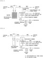
- the apparatus there are given an apparatus capable of performing bubbling supply of a precursor as illustrated in FIG. 1 and an apparatus including a vaporization chamber as illustrated in FIG. 2 .
- an apparatus capable of subjecting the reactive gas to plasma treatment as illustrated in FIG. 3 and FIG. 4 .
- the apparatus is not limited to single-substrate type apparatus as illustrated in FIG. 1 to FIG. 4 , and an apparatus capable of simultaneously processing a large number of substrates through use of a batch furnace may also be used.
- a thin-film produced through use of the thin-film forming raw material of the present invention may be formed as desired kinds of thin-films, such as thin-films of a metal, oxide ceramics, nitride ceramics, and glass, by appropriately selecting the other precursor, the reactive gas, and the production conditions. It has been known that the thin-films exhibit electrical characteristics, optical characteristics, and the like. Examples thereof include a metal scandium thin-film, a scandium oxide thin-film, a scandium alloy, and a scandium-containing composite oxide thin-film.
- An example of the scandium alloy is an Al-Sc alloy.
- Electrode materials for memory elements typified by DRAM elements
- resistance films diamagnetic films used for the recording layers of hard disks
- catalyst materials for polymer electrolyte fuel cells for polymer electrolyte fuel cells.
- a compound represented by the general formula (2) is also novel as a compound.
- the novel compound of the present invention is a compound, which has a low melting point, can be adapted to the ALD method, and is particularly suitable as a precursor for a method of producing a thin-film including a vaporization step, such as the CVD method.
- R 4 and R 5 each independently represent an alkyl group having 2 or 3 carbon atoms
- R 6 represents a hydrogen atom or an alkyl group having 1 to 4 carbon atoms.
- the alkyl group having 2 or 3 carbon atoms include an ethyl group, a n-propyl group, and an isopropyl group.
- R 4 or R 5 in the general formula (2) represents an ethyl group
- R 6 therein preferably represents a hydrogen atom because the compound has a high vapor pressure.
- An example of such compound is a compound in which both of R 4 and R 5 represent ethyl groups, and R 6 represents a hydrogen atom (Compound No. 7 above).
- the compound represented by the general formula (2) is not particularly limited by a production method therefor, and is produced by applying a well-known reaction.
- the compound may be obtained by, for example, a production method including: causing scandium chloride and an alkanedione compound having a corresponding structure to react with each other; and purifying the resultant through distillation.
- novel compound represented by the general formula (2) include compounds represented by Compounds No. 7 to No. 18 above.
- a scandium oxide thin-film was produced on a silicon wafer by the ALD method under the following conditions through use of an apparatus illustrated in FIG. 1 with Compound No. 7 being used as a raw material, which was used in an atomic layer deposition method.
- the obtained thin-film was scandium oxide, and its residual carbon content was less than 1.0 atom%.
- the average film thickness was 25.7 nm, and the average film thickness obtained per cycle was 0.05 nm.
- a scandium oxide thin-film was produced under the same conditions as those in Example 2 except that Compound No. 1 was used as a raw material, which was used in an atomic layer deposition method.
- the composition of the obtained thin-film was checked by X-ray photoelectron spectroscopy, the obtained thin-film was scandium oxide, and its residual carbon content was less than 1.0 atom%.
- the average film thickness was 15.5 nm, and the average film thickness obtained per cycle was 0.03 nm.
- a scandium oxide thin-film was produced under the same conditions as those in Example 2 except that Comparative Compound 1 was used as a raw material, which was used in an atomic layer deposition method.
- the composition of the obtained thin-film was checked by X-ray photoelectron spectroscopy, the obtained thin-film was scandium oxide, and its residual carbon content was 5.0 atom%.
- the average film thickness was 5.1 nm, and the average film thickness obtained per cycle was 0.01 nm.
Landscapes
- Chemical & Material Sciences (AREA)
- Organic Chemistry (AREA)
- General Chemical & Material Sciences (AREA)
- Chemical Kinetics & Catalysis (AREA)
- Engineering & Computer Science (AREA)
- Materials Engineering (AREA)
- Mechanical Engineering (AREA)
- Metallurgy (AREA)
- Inorganic Chemistry (AREA)
- Chemical Vapour Deposition (AREA)
- Formation Of Insulating Films (AREA)
- Compounds Of Alkaline-Earth Elements, Aluminum Or Rare-Earth Metals (AREA)
- Compositions Of Oxide Ceramics (AREA)
- Chemically Coating (AREA)
Applications Claiming Priority (2)
| Application Number | Priority Date | Filing Date | Title |
|---|---|---|---|
| JP2019071820 | 2019-04-04 | ||
| PCT/JP2020/014047 WO2020203783A1 (fr) | 2019-04-04 | 2020-03-27 | Matière première permettant la formation d'un film mince, procédé de production d'un film mince et composé de scandium |
Publications (2)
| Publication Number | Publication Date |
|---|---|
| EP3951006A1 true EP3951006A1 (fr) | 2022-02-09 |
| EP3951006A4 EP3951006A4 (fr) | 2023-01-11 |
Family
ID=72668437
Family Applications (1)
| Application Number | Title | Priority Date | Filing Date |
|---|---|---|---|
| EP20784999.3A Pending EP3951006A4 (fr) | 2019-04-04 | 2020-03-27 | Matière première permettant la formation d'un film mince, procédé de production d'un film mince et composé de scandium |
Country Status (6)
| Country | Link |
|---|---|
| US (1) | US20220213592A1 (fr) |
| EP (1) | EP3951006A4 (fr) |
| JP (1) | JP7573514B2 (fr) |
| KR (1) | KR102768702B1 (fr) |
| TW (1) | TWI824133B (fr) |
| WO (1) | WO2020203783A1 (fr) |
Families Citing this family (1)
| Publication number | Priority date | Publication date | Assignee | Title |
|---|---|---|---|---|
| WO2025169766A1 (fr) * | 2024-02-09 | 2025-08-14 | 東京エレクトロン株式会社 | Dispositif de formation de film, procédé de formation de film et procédé de traitement de substrrat |
Family Cites Families (6)
| Publication number | Priority date | Publication date | Assignee | Title |
|---|---|---|---|---|
| JP2005179777A (ja) * | 2003-11-26 | 2005-07-07 | Showa Denko Kk | 金属酸化物薄膜形成用組成物およびβ−ジケトン金属錯体溶液の安定化方法 |
| DE112005000134T5 (de) * | 2004-02-18 | 2007-02-15 | Adeka Corp. | Alkoxidverbindung, Material für die Bildung eines dünnen Films und Verfahren für die Bildung eines dünnen Films |
| US7544596B2 (en) | 2005-08-30 | 2009-06-09 | Micron Technology, Inc. | Atomic layer deposition of GdScO3 films as gate dielectrics |
| GB0821616D0 (en) | 2008-11-26 | 2008-12-31 | Lytix Biopharma As | Compounds |
| JP2010189208A (ja) | 2009-02-16 | 2010-09-02 | Nippon Telegr & Teleph Corp <Ntt> | ダイヤモンド半導体及び作製方法 |
| TWI742092B (zh) * | 2016-06-13 | 2021-10-11 | 美商應用材料股份有限公司 | 用於ald、cvd與薄膜摻雜之鑭系、釔與鈧前驅物及使用方法 |
-
2020
- 2020-03-27 EP EP20784999.3A patent/EP3951006A4/fr active Pending
- 2020-03-27 KR KR1020217032561A patent/KR102768702B1/ko active Active
- 2020-03-27 US US17/600,886 patent/US20220213592A1/en not_active Abandoned
- 2020-03-27 WO PCT/JP2020/014047 patent/WO2020203783A1/fr not_active Ceased
- 2020-03-27 JP JP2021512008A patent/JP7573514B2/ja active Active
- 2020-04-01 TW TW109111163A patent/TWI824133B/zh active
Also Published As
| Publication number | Publication date |
|---|---|
| TW202104237A (zh) | 2021-02-01 |
| JP7573514B2 (ja) | 2024-10-25 |
| KR20210149732A (ko) | 2021-12-09 |
| WO2020203783A1 (fr) | 2020-10-08 |
| US20220213592A1 (en) | 2022-07-07 |
| TWI824133B (zh) | 2023-12-01 |
| EP3951006A4 (fr) | 2023-01-11 |
| JPWO2020203783A1 (fr) | 2020-10-08 |
| KR102768702B1 (ko) | 2025-02-14 |
Similar Documents
| Publication | Publication Date | Title |
|---|---|---|
| EP3783130A1 (fr) | Matériau source de formation de film mince de dépôt de couche atomique et procédé de production d'un film mince | |
| US11555044B2 (en) | Thin-film forming raw material for use in atomic layer deposition method, thin-film forming raw material, method for producing thin-film, and compound | |
| US20250109296A1 (en) | Thin-film forming raw material used in atomic layer deposition method and method of producing thin-film | |
| EP3712159B1 (fr) | Composé ruthénium, matière de départ pour formation de film mince, et procédé de fabrication de film mince | |
| US11623935B2 (en) | Raw material for forming thin film by atomic layer deposition method, method of producing thin film, and alkoxide compound | |
| US12415821B2 (en) | Tin compound, thin-film forming raw material containing said compound, thin film formed from said thin-film forming raw material, method of producing said thin film using said compound as precursor, and method of producing said thin film | |
| US12104245B2 (en) | Compound, thin-film forming raw material that contains said compound, and method of manufacturing thin film | |
| EP4130010B1 (fr) | Composé de zinc, matière première pour la formation de couche mince et procédés de production de couche mince | |
| EP4180417A1 (fr) | Composé alcoxyde, matériau de formation de couche mince et procédé de fabrication de couche mince | |
| US20240425975A1 (en) | Thin-film forming raw material, method of producing thin-film, thin-film, and molybdenum compound | |
| EP3951006A1 (fr) | Matière première permettant la formation d'un film mince, procédé de production d'un film mince et composé de scandium | |
| EP4067365B1 (fr) | Composé, matière première de formation de couche mince, et procédé de production de couche mince | |
| US12486573B2 (en) | Thin-film forming raw material, thin-film and method of producing thin-film | |
| US12509764B2 (en) | Thin-film forming raw material used in atomic layer deposition method, and method of producing thin-film | |
| US12577660B2 (en) | Compound, thin-film forming raw material, thin-film, and method of producing thin-film | |
| US12371778B2 (en) | Cobalt compound, thin-film forming raw material, thin-film, and method of producing thin-film | |
| US12264168B2 (en) | Ruthenium compound, thin-film forming raw material, and method of producing thin film | |
| EP4434994A1 (fr) | Matériau de formation de film mince destiné à être utilisé dans le dépôt de couche atomique, film mince, procédé de production de film mince et composé de ruthénium |
Legal Events
| Date | Code | Title | Description |
|---|---|---|---|
| STAA | Information on the status of an ep patent application or granted ep patent |
Free format text: STATUS: THE INTERNATIONAL PUBLICATION HAS BEEN MADE |
|
| PUAI | Public reference made under article 153(3) epc to a published international application that has entered the european phase |
Free format text: ORIGINAL CODE: 0009012 |
|
| STAA | Information on the status of an ep patent application or granted ep patent |
Free format text: STATUS: REQUEST FOR EXAMINATION WAS MADE |
|
| 17P | Request for examination filed |
Effective date: 20210923 |
|
| AK | Designated contracting states |
Kind code of ref document: A1 Designated state(s): AL AT BE BG CH CY CZ DE DK EE ES FI FR GB GR HR HU IE IS IT LI LT LU LV MC MK MT NL NO PL PT RO RS SE SI SK SM TR |
|
| DAV | Request for validation of the european patent (deleted) | ||
| DAX | Request for extension of the european patent (deleted) | ||
| RIN1 | Information on inventor provided before grant (corrected) |
Inventor name: HARANO, KAZUKI Inventor name: SATO, HARUYOSHI Inventor name: YAMADA, NAOKI |
|
| A4 | Supplementary search report drawn up and despatched |
Effective date: 20221209 |
|
| RIC1 | Information provided on ipc code assigned before grant |
Ipc: H01L 21/02 20060101ALI20221205BHEP Ipc: C07C 45/77 20060101ALI20221205BHEP Ipc: C23C 16/455 20060101ALI20221205BHEP Ipc: C23C 16/40 20060101ALI20221205BHEP Ipc: C07C 49/92 20060101AFI20221205BHEP |