EP3951765A1 - Registre à décalage et son procédé d'attaque, circuit d'attaque de grille, et dispositif d'affichage - Google Patents
Registre à décalage et son procédé d'attaque, circuit d'attaque de grille, et dispositif d'affichage Download PDFInfo
- Publication number
- EP3951765A1 EP3951765A1 EP19861299.6A EP19861299A EP3951765A1 EP 3951765 A1 EP3951765 A1 EP 3951765A1 EP 19861299 A EP19861299 A EP 19861299A EP 3951765 A1 EP3951765 A1 EP 3951765A1
- Authority
- EP
- European Patent Office
- Prior art keywords
- transistor
- signal
- coupled
- gate
- electrode
- Prior art date
- Legal status (The legal status is an assumption and is not a legal conclusion. Google has not performed a legal analysis and makes no representation as to the accuracy of the status listed.)
- Granted
Links
Images









Classifications
-
- G—PHYSICS
- G09—EDUCATION; CRYPTOGRAPHY; DISPLAY; ADVERTISING; SEALS
- G09G—ARRANGEMENTS OR CIRCUITS FOR CONTROL OF INDICATING DEVICES USING STATIC MEANS TO PRESENT VARIABLE INFORMATION
- G09G3/00—Control arrangements or circuits, of interest only in connection with visual indicators other than cathode-ray tubes
- G09G3/20—Control arrangements or circuits, of interest only in connection with visual indicators other than cathode-ray tubes for presentation of an assembly of a number of characters, e.g. a page, by composing the assembly by combination of individual elements arranged in a matrix no fixed position being assigned to or needed to be assigned to the individual characters or partial characters
-
- G—PHYSICS
- G11—INFORMATION STORAGE
- G11C—STATIC STORES
- G11C19/00—Digital stores in which the information is moved stepwise, e.g. shift registers
- G11C19/28—Digital stores in which the information is moved stepwise, e.g. shift registers using semiconductor elements
-
- G—PHYSICS
- G09—EDUCATION; CRYPTOGRAPHY; DISPLAY; ADVERTISING; SEALS
- G09G—ARRANGEMENTS OR CIRCUITS FOR CONTROL OF INDICATING DEVICES USING STATIC MEANS TO PRESENT VARIABLE INFORMATION
- G09G2300/00—Aspects of the constitution of display devices
- G09G2300/04—Structural and physical details of display devices
- G09G2300/0404—Matrix technologies
- G09G2300/0408—Integration of the drivers onto the display substrate
-
- G—PHYSICS
- G09—EDUCATION; CRYPTOGRAPHY; DISPLAY; ADVERTISING; SEALS
- G09G—ARRANGEMENTS OR CIRCUITS FOR CONTROL OF INDICATING DEVICES USING STATIC MEANS TO PRESENT VARIABLE INFORMATION
- G09G2300/00—Aspects of the constitution of display devices
- G09G2300/04—Structural and physical details of display devices
- G09G2300/0421—Structural details of the set of electrodes
- G09G2300/0426—Layout of electrodes and connections
-
- G—PHYSICS
- G09—EDUCATION; CRYPTOGRAPHY; DISPLAY; ADVERTISING; SEALS
- G09G—ARRANGEMENTS OR CIRCUITS FOR CONTROL OF INDICATING DEVICES USING STATIC MEANS TO PRESENT VARIABLE INFORMATION
- G09G2300/00—Aspects of the constitution of display devices
- G09G2300/08—Active matrix structure, i.e. with use of active elements, inclusive of non-linear two terminal elements, in the pixels together with light emitting or modulating elements
-
- G—PHYSICS
- G09—EDUCATION; CRYPTOGRAPHY; DISPLAY; ADVERTISING; SEALS
- G09G—ARRANGEMENTS OR CIRCUITS FOR CONTROL OF INDICATING DEVICES USING STATIC MEANS TO PRESENT VARIABLE INFORMATION
- G09G2310/00—Command of the display device
- G09G2310/02—Addressing, scanning or driving the display screen or processing steps related thereto
- G09G2310/0264—Details of driving circuits
- G09G2310/0267—Details of drivers for scan electrodes, other than drivers for liquid crystal, plasma or OLED displays
-
- G—PHYSICS
- G09—EDUCATION; CRYPTOGRAPHY; DISPLAY; ADVERTISING; SEALS
- G09G—ARRANGEMENTS OR CIRCUITS FOR CONTROL OF INDICATING DEVICES USING STATIC MEANS TO PRESENT VARIABLE INFORMATION
- G09G2310/00—Command of the display device
- G09G2310/02—Addressing, scanning or driving the display screen or processing steps related thereto
- G09G2310/0264—Details of driving circuits
- G09G2310/0286—Details of a shift registers arranged for use in a driving circuit
-
- G—PHYSICS
- G09—EDUCATION; CRYPTOGRAPHY; DISPLAY; ADVERTISING; SEALS
- G09G—ARRANGEMENTS OR CIRCUITS FOR CONTROL OF INDICATING DEVICES USING STATIC MEANS TO PRESENT VARIABLE INFORMATION
- G09G2310/00—Command of the display device
- G09G2310/08—Details of timing specific for flat panels, other than clock recovery
-
- G—PHYSICS
- G09—EDUCATION; CRYPTOGRAPHY; DISPLAY; ADVERTISING; SEALS
- G09G—ARRANGEMENTS OR CIRCUITS FOR CONTROL OF INDICATING DEVICES USING STATIC MEANS TO PRESENT VARIABLE INFORMATION
- G09G2320/00—Control of display operating conditions
- G09G2320/02—Improving the quality of display appearance
- G09G2320/0209—Crosstalk reduction, i.e. to reduce direct or indirect influences of signals directed to a certain pixel of the displayed image on other pixels of said image, inclusive of influences affecting pixels in different frames or fields or sub-images which constitute a same image, e.g. left and right images of a stereoscopic display
- G09G2320/0214—Crosstalk reduction, i.e. to reduce direct or indirect influences of signals directed to a certain pixel of the displayed image on other pixels of said image, inclusive of influences affecting pixels in different frames or fields or sub-images which constitute a same image, e.g. left and right images of a stereoscopic display with crosstalk due to leakage current of pixel switch in active matrix panels
Definitions
- the present disclosure relates to the field of displaying, and particularly to a shift register and a driving method thereof, a gate driving circuit, and a display device.
- a GOA Gate Driver on Array
- TFT Thin Film Transistor
- the embodiment of the present disclosure provides a shift register, including: an input circuit, configured to be coupled to an input signal end and a second clock signal end, respectively; a first transistor, where a first electrode of the first transistor is coupled to an output end of the input circuit, and the first transistor is a double-gate type transistor; a first gate of the first transistor is configured to be coupled to a first reference signal end, and a second gate of the first transistor is configured to be coupled to a first threshold control signal end; and an output circuit, configured to be coupled to a first clock signal end and a signal output end, respectively, where a control end of the output circuit is coupled to a second electrode of the first transistor.
- the input circuit includes: a single-gate second transistor.
- a gate of the second transistor is configured to be coupled to the second clock signal end.
- a first electrode of the second transistor is configured to be coupled to the input signal end.
- a second electrode of the second transistor is coupled to the first electrode of the first transistor.
- the second gate of the first transistor is coupled to the gate of the second transistor; or, the second gate of the first transistor is coupled to the first electrode of the second transistor.
- the input circuit includes: a double-gate type second transistor.
- a first gate of the second transistor is configured to be coupled to the second clock signal end, and a second gate of the second transistor is configured to be coupled to a second threshold control signal end.
- a first electrode of the second transistor is configured to be coupled to the input signal end, and a second electrode of the second transistor is coupled to the first electrode of the first transistor.
- the second gate of the second transistor is coupled to the first gate of the second transistor; or, the second gate of the second transistor is coupled to the first electrode of the second transistor.
- the second gate of the first transistor is coupled to the first gate of the second transistor; or, the second gate of the first transistor is coupled to the first electrode of the second transistor.
- the shift register further includes: a fifth transistor, a sixth transistor, a seventh transistor, and a first capacitor.
- a gate of the fifth transistor is configured to be coupled to the second clock signal end.
- a first electrode of the fifth transistor is configured to be coupled to the first reference signal end.
- a second electrode of the fifth transistor is coupled to a gate of the seventh transistor.
- a gate of the sixth transistor is configured to be coupled to the first electrode of the first transistor.
- a first electrode of the sixth transistor is configured to be coupled to the second clock signal end.
- a second electrode of the sixth transistor is coupled to the gate of the seventh transistor.
- a first electrode of the seventh transistor is configured to be coupled to the second reference signal end, and a second electrode of the seventh transistor is coupled to the signal output end.
- a first end of the first capacitor is coupled to the gate of the seventh transistor, and a second end of the first capacitor is configured to be coupled to the second reference signal end.
- the shift register further includes: a pull-up control circuit.
- a first control end of the pull-up control circuit is configured to be coupled to the first clock signal end.
- a second control end of the pull-up control circuit is coupled to the gate of the seventh transistor.
- An input end of the pull-up control circuit is configured to be coupled to the second reference signal end.
- An output end of the pull-up control circuit is coupled to the first electrode of the first transistor.
- the pull-up control circuit includes: a third transistor and a single-gate type fourth transistor.
- a gate of the third transistor is configured to be coupled to the first clock signal end.
- a first electrode of the third transistor is coupled to the first electrode of the first transistor.
- a second electrode of the third transistor is coupled to a first electrode of the fourth transistor.
- a gate of the fourth transistor is coupled to the gate of the seventh transistor, and a second electrode of the fourth transistor is configured to be coupled to the second reference signal end.
- the pull-up control circuit includes: a third transistor and a double-gate type fourth transistor.
- a gate of the third transistor is configured to be coupled to the first clock signal end.
- a first electrode of the third transistor is coupled to the first electrode of the first transistor.
- a second electrode of the third transistor is coupled to a first electrode of the fourth transistor.
- a first gate of the fourth transistor is coupled to the gate of the seventh transistor.
- a second gate of the fourth transistor is configured to be coupled to a third threshold control signal end.
- a second electrode of the fourth transistor is configured to be coupled to the second reference signal end.
- the second gate of the fourth transistor is coupled to the gate of the seventh transistor; or, the second gate of the fourth transistor is coupled to the gate of the fifth transistor.
- the output circuit includes: an eighth transistor and a second capacitor.
- a gate of the eighth transistor is configured to be coupled to the second electrode of the first transistor.
- a first electrode of the eighth transistor is configured to be coupled to the first clock signal end.
- a second electrode of the eighth transistor is coupled to the signal output end.
- a first end of the second capacitor is coupled to the second electrode of the first transistor, and a second end of the second capacitor is configured to be coupled to the signal output end.
- the first threshold control signal end is configured to receive a signal at least having a level opposite to a level of the signal of the first reference signal end.
- the second threshold control signal end is configured to receive the signal at least having a level opposite to a level of the signal of the first reference signal end.
- the third threshold control signal end is configured to receive the signal at least having a level opposite to a level of the signal of the first reference signal end.
- At least one of the first threshold control signal end, the second threshold control signal end, and the third threshold control signal end is configured to receive a clock signal which is the same as a time sequence of the second clock signal end.
- At least one of the first threshold control signal end, the second threshold control signal end, and the third threshold control signal end is configured to receive a fixed voltage signal.
- the embodiment of the present disclosure further provides a gate driving circuit, including a plurality of the above shift registers that are cascaded.
- An input signal terminal of a first stage of shift register is configured to be coupled to a frame trigger signal end.
- an input signal end of a next stage of shift register is configured to be coupled to a signal output end of a previous stage of shift register.
- the embodiment of the present disclosure further provides a display device, including the above-mentioned gate driving circuit.
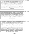
- the embodiment of the present disclosure further provides a driving method of the above-mentioned shift register, including: at an input phase, controlling, by the input circuit, a level of a signal of the first electrode of the first transistor according to signals of the input signal end and the second clock signal end, switching on the first transistor, and providing, by the output circuit in response to a signal of the second electrode of the first transistor, a signal of the first clock signal end to the signal output end; at an output phase, enabling a threshold voltage of the first transistor to move in response to a signal of the first threshold control signal end, switching off the first transistor, and providing, by the output circuit in response to the signal of the second electrode of the first transistor, the signal of the first clock signal end to the signal output end, where a level of a signal of the first threshold control signal end is opposite to a level of a signal of the first reference signal end.
- the input phase further includes: providing, by the fifth transistor in response to the signal of the second clock signal end, the signal of the first reference signal end to a gate of a seventh transistor; providing, by a sixth transistor in response to the signal of the first electrode of the first transistor, the signal of the second clock signal end to the gate of the seventh transistor; and providing, by the seventh transistor in response to a signal of the gate of the seventh transistor, the signal of the second reference signal end to the signal output end.
- the driving method further includes: at a reset phase, controlling, by the input circuit, the level of the signal of the first electrode of the first transistor according to the signals of the input signal end and the second clock signal end; switching on, by the first transistor, the input circuit and the output circuit; providing, by the fifth transistor in response to the signal of the second clock signal end, the signal of the first reference signal end to the gate of the seventh transistor; and providing, by a seventh transistor in response to the signal of the gate of the seventh transistor, the signal of the second reference signal end to the signal output end.
- a threshold voltage of the second transistor moves in response to a signal of a second threshold control signal end, and the second transistor is switched off; and a threshold voltage of a fourth transistor moves in response to a signal of a third threshold control signal end, and the fourth transistor is switched off.
- a shift register may include transistors M01 to M08, and capacitors C01 to C02.
- a signal time sequence diagram corresponding to the shift register shown in Fig. 1 is as shown in Fig. 2 .
- the transistor M02 and the transistor M05 are switched on under the control of the signal of a clock signal end CK.
- the switched-on transistor M05 provides a low-level signal of a signal end VSS to a pull-down node PD to enable the signal of the pull-down node PD to be the low-level signal, so as to control the transistor M04 and the transistor M07 to be switched on.
- the transistor M03 is switched off under the control of the signal of a clock signal end CKB.
- the switched-on transistor M07 provides a high-level signal of a signal end VDD to a signal output end OP to enable the signal output end OP to output the high-level signal.
- the switched-on transistor M02 provides a low-level signal of an input signal end IP to a second pull-up node PU_2 to enable the signal of the second pull-up node PU_2 to be the low-level signal.
- the transistor M06 is switched on under the control of the signal of the second pull-up node PU_2, so as to provide the low-level signal of the clock signal end CK to the pull-down node PD. Since the transistor M01 satisfies V gs01 ⁇ Vth01 , so that the transistor M01 is switched on. At this time, an electrode, connected with a first pull-up node PU_1, of the transistor M01 is used as a source.
- V gs01 represents a voltage difference between the gate and the source of the transistor M01
- V th01 represents a threshold voltage of the transistor M01.
- the switched-on transistor M01 switches on the second pull-up node PU_2 and the first pull-up node PU_1, thereby enabling the signal of the first pull-up node PU_1 to be the low-level signal to control the transistor M08 to be switched on.
- the switched-on transistor M08 provides the high-level signal of the clock signal end CKB to the signal output end OP to enable the signal output end OP to output the high-level signal.
- the voltage of the low-level signal of the first pull-up node PU_1 may be the same as the voltage of the signal of the signal end VSS. Due to the reason of the threshold voltage of the transistor M01, the voltage of the low-level signal of the first pull-up node PU_1 may be less than the voltage of the low-level signal of the second pull-up node PU_2.
- specific voltages may be designed and determined according to an actual application environment, and are not limited here.
- the transistor M02 and the transistor M05 are switched off under the control of the high-level signal of the clock signal end CK, and the transistor M03 is also switched off under the control of the high-level signal of the clock signal end CKB.
- the first pull-up node PU_1 is kept at the low-level signal under the action of the capacitor C01.
- an electrode with relatively high voltage may be used as the source of a transistor. Therefore, at this phase, the electrode, electrically connected to the second pull-up node PU_2, of the transistor M01 is used as the source of the transistor M01, so that the transistor M01 may satisfy V gs01 ⁇ V th01 .
- the transistor M01 is switched on, so that the signal of the second pull-up node PU_2 is the low-level signal.
- the transistor M06 is switched on under the control of the signal of the second pull-up node PU_2 to provide the high-level signal of the clock signal end CKB to the pull-down node PD, so as to enable the signal of the pull-down node PD to be the high-level signal to control the transistor M04 and the transistor M07 to be switched off.
- the transistor M08 is switched on under the control of the signal of the first pull-up node PU_1 to provide the high-level signal of the clock signal end CKB to the signal output end OP to enable the signal output end OP to output the high-level signal.
- the transistor M02 and the transistor M05 are switched off under the control of the high-level signal of the clock signal end CK, and the first pull-up node PU_1 is kept at the low-level signal under the action of the capacitor C01 to control the transistor M08 to be switched on, thereby providing the low-level signal of the clock signal end CKB to the signal output end OP.
- the level of the first pull-up node PU_1 is further pulled down to control the transistor M08 to be completely switched on as much as possible to provide the low-level signal of the clock signal end CKB to the signal output end OP, so that the signal output end OP outputs the low-level signal.
- the transistor M01 undergoes long-time accumulation of leakage, which causes a phenomenon of leakage of the level of the first pull-up node PU_1 that is further pulled down and causes the level of the first pull-up node PU_1 to rise, so that the transistor M08 may not be switched on completely, leading to an abnormality in the signal output by the signal output end OP.
- the transistors M01, M02, and M04 undergo the long-term accumulation of leakage, so that the levels of PU_2 and PU_1 would rise, leading to the abnormality in the signal output by the signal output end OP.
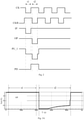
- Fig. 3A is a simulation diagram of the signal output by the signal output end OP of the shift register shown in Fig. 1 under the control of the signal shown in Fig. 2 .
- Fig. 3B is a simulation diagram of the signal output by the first pull-up node PU_1 of the shift register shown in Fig. 1 under the control of the signal shown in Fig. 2 .
- the X-coordinate represents time
- the Y-coordinate represents voltage. It can be known in combination with Fig.
- the leakage of the level of the first pull-up node PU_1 causes the level of the first pull-up node PU_1 to rise, so that the level of the signal output by the signal output end OP also rises, thus leading to the abnormality in the signal output by the signal output end OP. Furthermore, due to the influence of the leakage, the above shift register is not conductive to being configured in the low-frequency (such as 1 Hz) driven display device.
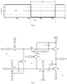
- the embodiment of the present disclosure provides some shift registers, as shown in Fig. 4A .
- the register includes an input circuit 10, a first transistor M1 and an output circuit 20.
- the input circuit 10 is configured to be coupled to an input signal end IP and a second clock signal end CK2, respectively.
- a first electrode of the first transistor M1 is coupled to an output end of the input circuit 10.
- the first transistor M1 is a double-gate type transistor.
- a first gate of the first transistor M1 is configured to be coupled to a first reference signal end VREF1, and a second gate of the first transistor M1 is configured to be coupled to a first threshold control signal end VS1.
- the output circuit 20 is configured to be coupled to a first clock signal end CK1 and a signal output end OP, respectively.
- a control end of the output circuit 20 is coupled to a second electrode of the first transistor M1.
- the first transistor is set as a double-gate type transistor.
- the first gate of the first transistor receives the first reference signal end, and the second gate of the first transistor receives the first threshold control signal end, so that the first transistor may be switched on at an input phase, a reset phase, and a reset holding phase.
- the signal of the first threshold control signal end controls a threshold voltage V th1 of the first transistor to enable the threshold voltage V th1 of the first transistor to move, so as to enable the first transistor to be switched off as much as possible at the output phase, which may keep the level of the signal of the first pull-up node to be stabilized and avoid the influence of leakage on the signal of the first pull-up node. Therefore, the stability of the signal output by the signal output end is improved.
- the shift register is favorably applied to the low-frequency driven display device, and is conductive to reducing the power consumption.
- the first pull-up node PU_1 is located between the control end of the output circuit 20 and the second electrode of the first transistor M1.
- the second pull-up node PU_2 is located between the output end of the input circuit 10 and the first electrode of the first transistor M1.
- the first pull-up node PU_1 and the second pull-up node PU_2 are virtual nodes in the shift register. The two nodes are only to facilitate the description of the structure of the shift register and transmission of signals. The specific structure of the shift register and the transmission of the signals may be determined according to a coupling mode between various transistors and capacitors in the shift register.
- the input circuit 10 is configured to control the level of the signal of the second pull-up node PU_2 according to the input signal end IP and the second clock signal end CK2.
- the signal of the input signal end IP may be input through the input circuit 10.
- the output circuit 20 is configured to provide the signal of the first clock signal end CK1 to the signal output end OP in response to the signal of the first pull-up node PU_1.
- the signal of the first clock signal end CK1 may be output through the output circuit 20.
- the second pull-up node PU_2 is coupled to the first pull-up node PU_1 through the first transistor M1.
- the first electrode of the first transistor M1 is coupled to the second pull-up node PU_2, and the second electrode of the first transistor M1 is coupled to the first pull-up node PU_1.
- the input circuit 10 may include: a single-gate type second transistor M2.
- the gate of the second transistor M2 is configured to be coupled to the second clock signal end CK2.
- the first electrode of the second transistor M2 is configured to be coupled to the input signal end IP.
- the second electrode of the second transistor M2 is coupled to the first electrode of the first transistor M1, that is, the second electrode of the second transistor M2 is coupled to the second pull-up node PU_2.
- the second transistor M2 in an on state under the control of the signal of the second clock signal end CK2 may provide the signal of the input signal end IP to the first electrode (i.e., the second pull-up node PU_2) of the first transistor M1, so as to control the level of the signal of the first electrode (i.e., the second pull-up node PU_2) of the first transistor M1.
- the shift register further includes: a fifth transistor M5, a sixth transistor M6, a seventh transistor M7, and a first capacitor C1.
- the gate of the fifth transistor M5 is configured to be coupled to the second clock signal end CK2.
- the first electrode of the fifth transistor M5 is configured to be coupled to the first reference signal end VREF1.
- the second electrode of the fifth transistor M5 is coupled to the gate of the seventh transistor M7 (i.e., the pull-down node PD).
- the gate of the sixth transistor M6 is coupled to the first electrode (i.e., the second pull-up node PU_2) of the first transistor M1.
- the first electrode of the sixth transistor M6 is configured to be coupled to the second clock signal end CK2.
- the second electrode of the sixth transistor M6 is coupled to the gate (i.e., the pull-down node PD) of the seventh transistor M7.
- the first electrode of the seventh transistor M7 is configured to be coupled to the second reference signal end VREF2, and the second electrode of the seventh transistor M7 is coupled to the signal output end OP.
- the first end of the first capacitor C1 is coupled to the gate (i.e., the pull-down node PD) of the seventh transistor M7, and the second end of the first capacitor C1 is configured to be coupled to the second reference signal end VREF2.
- the fifth transistor M5 in an on state under the control of the signal of the second clock signal end CK2 may provide the signal of the first reference signal end VREF1 to the gate (i.e., the pull-down node PD) of the seventh transistor M7.
- the sixth transistor M6 in an on state under the control of the signal of the first electrode of the first transistor M1 may provide the signal of the second clock signal end CK2 to the gate (i.e., the pull-down node PD) of the seventh transistor M7.
- the seventh transistor M7 in an on state under the control of the signal of its gate (i.e., the pull-down node PD) may provide the signal of the second reference signal terminal VREF2 to the signal output end OP for coupling.
- the first capacitor C1 may store the signal input to the gate (i.e., the pull-down node PD) of the seventh transistor M7 and the signal of the second reference signal end VREF2, and keep the signals stable.
- the shift register may further include: a pull-up control circuit 30.
- the first control end of the pull-up control circuit 30 is configured to be coupled to the first clock signal end CK1.
- the second control end of the pull-up control circuit 30 is coupled to the gate of the seventh transistor M7.
- the input end of the pull-up control circuit 30 is configured to be coupled to the second reference signal end VREF2.
- the output end of the pull-up control circuit 30 is coupled to the first electrode of the first transistor M1.
- the pull-up control circuit 30 is configured to provide the signal of the second reference signal end VREF2 to the first electrode (i.e., the second pull-up node PU_2) of the first transistor M1 in response to the signal of the first clock signal end CK1 and the signal of the gate (i.e., the pull-down node PD) of the seventh transistor M7.
- the pull-up control circuit 30 may include: a third transistor M3 and a single-gate type fourth transistor M4.
- the gate of the third transistor M3 is configured to be coupled to the first clock signal end CK1.
- the first electrode of the third transistor M3 is coupled to the first electrode (i.e., the second pull-up node PU_2) of the first transistor M1.
- the second electrode of the third transistor M3 is coupled to the first electrode of the fourth transistor M4.
- the gate of the fourth transistor M4 is coupled to the gate (i.e., the pull-down node PD) of the seventh transistor M7, and the second electrode of the fourth transistor M4 is configured to be coupled to the second reference signal end VREF2.
- the fourth transistor M4 in an on state under the control of the signal of the gate (i.e., the pull-down node PD) of the seventh transistor M7 may provide the signal of the second reference signal terminal VREF2 to the first electrode of the fourth transistor M4.
- the third transistor M3 in an on state under the control of the signal of the first clock signal end CK1 may switch on the first electrode (i.e., the second pull-up node PU_2) of the first transistor M1 and the first electrode of the fourth transistor M4.
- the output circuit 20 may include: an eighth transistor M8 and a second capacitor C2.
- the gate of the eighth transistor M8 is coupled to the second electrode (i.e., the first pull-up node PU_1) of the first transistor M1.
- the first electrode of the eighth transistor M8 is coupled to the first clock signal end CK1.
- the second electrode of the eighth transistor M8 is coupled to the signal output end OP.
- the first end of the second capacitor C2 is coupled to the second electrode (i.e., the first pull-up node PU_1) of the first transistor M1, and the second end of the second capacitor C2 is coupled to the signal output end OP.
- the eighth transistor M8 in an on state under the control of the signal of the second electrode (i.e., the first pull-up node PU_1) of the first transistor M1 may provide the signal of the first clock signal end CK1 to the signal output end OP.
- the second capacitor C2 may store the signal input to the second electrode (i.e., the first pull-up node PU_1) of the first transistor M1 and the signal input to the signal output end OP, and keep the signals stable, and may keep the stability of a voltage difference between the first pull-up node PU_1 and the signal output end OP when the second electrode (i.e., the first pull-up node PU_1) of the first transistor M1 is in a levitated state.
- the first electrode of each of the above transistors may be used as its source, and the second source may be used as its drain, or the first electrode of each of the above transistors may be used as its drain, and the second electrode may be used as its source. No specific distinction is made here.
- each of the transistors mentioned in the above embodiments of the present disclosure may be a TFT, or a MOS (Metal Oxide Semiconductor) field-effect transistor, and is not limited herein.
- all the transistors may be P-type transistors.
- the P-type transistor is switched on when a voltage difference V gs between the gate and the source of the P-type transistor and a threshold voltage V th of the P-type transistor satisfy a relationship V gs ⁇ V th .
- the first transistor M1 may be the P-type transistor, which is switched on when the relationship between the voltage difference V gs1 between the gate and the source of the first transistor M1 and the threshold voltage V th1 of the first transistor M1 satisfies the formula: V gs1 ⁇ V th1 .
- the P-type transistors are taken for example for illustration.
- the transistors are N-type transistors
- the design principle is the same as that of the present disclosure, and also falls within the scope of the protection of the present disclosure.
- the N-type transistor is switched on when a voltage difference V gs between the gate and the source of the N-type transistor and a threshold voltage V th of the N-type transistor satisfy a relationship V gs >V th .
- the first transistor M1 may be the N-type transistor, which is switched on when the relationship between the voltage difference V gs1 between the gate and the source of the first transistor M1 and the threshold voltage V th1 of the first transistor M1 satisfies the formula: V gs1 >V th1 .
- a gate insulating layer would be arranged between the gate of a transistor and an active layer.
- a dominate gate in a double-gate type transistor may be determined by adjusting the thickness of the gate insulating layer.
- the first gate of the first transistor is enabled to be dominated by adjusting the thickness of the gate insulating layer, so that the first transistor M1 is switched on when the relationship between the voltage difference V gs1 between the gate (i.e., the first gate) and the source of the first transistor M1 and the threshold voltage V th1 of the first transistor M1 satisfies the formula: V gs1 ⁇ V th1 .
- the voltage difference represented by V gs1 between the first gate and the source of the first transistor M1 is illustrated below as an example.
- the first threshold control signal end is configured to receive a signal at least having a level opposite to the level of the signal of the first reference signal end VREF1.
- the signal of the first reference signal end VREF1 when an effective pulse signal of the input signal end IP is a low-level signal, the signal of the first reference signal end VREF1 is a low-level signal, and the signal of the second reference signal end VREF2 is a high-level signal.
- the first threshold control signal end VS1 is configured to receive a signal at least having a high-level.
- the signal of the first reference signal end VREF1 when the effective pulse signal of the input signal end IP is a high-level signal, the signal of the first reference signal end VREF1 is a high-level signal, and the signal of the second reference signal end VREF2 is a low-level signal.
- the first threshold control signal end VS1 is configured to receive a signal at least having a low-level. It should be noted that as shown in Fig. 5a , the effective pulse signal of the input signal end IP refers to a low-level signal input to the second transistor M2 within one frame of time, so as to control the shift register to do output work.
- the P-type transistor is switched off under the action of the high-level signal, and is switched on under the action of the low-level signal.
- the N-type transistor is switched on under the action of the high-level signal, and is switched off under the action of the low-level signal.
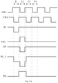
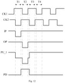
- the shift register shown in Fig. 4A is exemplified below to describe the working process of the above-mentioned shift register provided by the embodiment of the present disclosure in combination with the signal time sequence diagram shown in Fig. 5A .
- 1 represents the high-level signal
- 0 represents the low-level signal.
- 1 and 0 are logic levels, which are merely to better explain the specific working process of the embodiment of the present disclosure, instead of indicating the voltage applied to the gate of each transistor during the specific implementation.
- an input phase T1, an output phase T2, a reset phase T3 and a reset holding phase T4 in the signal time sequence diagram as shown in Fig. 5A are selected.
- the signal time sequence diagram shown in Fig. 5A is only a working process of a certain shift register in a current frame.
- the working processes of the shift register in other frames are basically the same as the working process in the current frame, respectively, and will not be repeatedly described here.
- the switched-on fifth transistor M5 may provide the low-level signal of the first reference signal end VREF1 to the pull-down node PD to enable the signal of the pull-down node PD to be the low-level signal, so as to control the fourth transistor M4 and the seventh transistor M7 to be switched on.
- the switched-on seventh transistor M7 may provide the high-level signal of the second reference signal end VREF2 to the signal output end OP to enable the signal output end OP to output the high-level signal.
- the switched-on second transistor M2 may provide the low-level signal of the input signal end IP to the second pull-up node PU_2 to enable the signal of the second pull-up node PU_2 to be the low-level signal.
- the signal of the first pull-up node PU_1 is the high-level signal, so that an electrode, connected to the first pull-up node PU_1, of the first transistor M1 in the current frame is used as the source.
- the switched-on first transistor M1 switches on the second pull-up node PU_2 and the first pull-up node PU_1, thereby timely enabling the signal of the first pull-up node PU_1 to be the low-level signal to control the eighth transistor M8 to be switched on.
- the switched-on eighth transistor M8 provides the high-level signal of the first clock signal end CK1 to the signal output end OP to enable the signal output end OP to output the high-level signal.
- the signal of the second pull-up node PU_2 is the low-level signal, so as to control the sixth transistor M6 to be switched on.
- the switched-on sixth transistor M6 may provide the high-level signal of the second clock signal end CK2 to the pull-down node PD to enable the signal of the pull-down node PD to be the high-level signal, so as to control the fourth transistor M4 and the seventh transistor M7 to be switched off.
- the eighth transistor M8 is switched on under the control of the signal of the first pull-up node PU_1 to provide the high-level signal of the first clock signal end CK1 to the signal output end OP to enable the signal output end OP to output the high-level signal.
- the second transistor M2 and the fifth transistor M5 are both switched off, and then the first pull-up node PU_1 is kept at the low-level signal under the action of the second capacitor C2 to control the eighth transistor M8 to be switched on, thereby providing the low-level signal of the first clock signal end CK1 to the signal output end OP to enable the signal output end OP to output the low-level signal.
- the level of the first pull-up node PU_1 is further pulled down to control the eighth transistor M8 to be completely switched on as much as possible to provide the low-level signal of the first clock signal end CK1 to the signal output end OP, so that the signal output end OP outputs the low-level signal.
- the voltage of the gate of the first transistor M1 is the voltage of the low-level signal, and the voltage of the source of the first transistor M1 is the voltage of the low-level signal, so that the first transistor M1 may not satisfy V gs1 ⁇ V th1 , and then is switched off. Therefore, the level of the first pull-up node PU_1 may be kept stable, and the phenomenon of an unstable output of the signal output end OP due to the rise of the level, caused by leakage, of the first pull-up node PU_1 is avoided.
- the signal of the pull-down node PD may be kept being the high-level signal, thereby controlling the fourth transistor M4 and the seventh transistor M7 to be both switched off and avoiding adverse effect on the signal output by the signal output end OP.
- the switched-on second transistor M2 may provide the high-level signal of the input signal end IP to the second pull-up node PU_2 to enable the signal of the second pull-up node PU_2 to be the high-level signal, so as to control the sixth transistor M6 to be switched off. Furthermore, at this phase, an electrode, electrically connected to the second pull-up node PU_2, of the first transistor M1 is used as the source. The first transistor M1 is switched on since it satisfies V gs1 ⁇ V th1 .
- the switched-on fifth transistor M5 may provide the low-level signal of the first reference signal end VREF1 to the pull-down node PD to enable the signal of the pull-down node PD to be the low-level signal, so as to control the fourth transistor M4 and the seventh transistor M7 to be switched on. Furthermore, since CK1 is equal to 1, the third transistor M3 is switched off.
- the switched-on seventh transistor M7 may provide the high-level signal of the second reference signal end VREF2 to the signal output end OP to enable the signal output end OP to output the high-level signal.
- an electrode, electrically connected to the second pull-up node PU_2, of the first transistor M1 is used as the source.
- the first transistor M1 is switched on since it satisfies V gs1 ⁇ V th1 . Therefore, the second pull-up node PU_2 and the first pull-up node PU_1 are switched, so as to control the eighth transistor M8 to be switched off.
- the switched-on seventh transistor M7 may provide the high-level signal of the second reference signal end VREF2 to the signal output end OP to enable the signal output end OP to output the high-level signal.
- a buffer phase is provided between the input phase T1 and the output phase T2, between the output phase T2 and the reset phase T3, and between the reset phase T3 and the reset holding phase T4, respectively.
- the characteristics of the transistors in the shift register may be stabilized, and the next working phase is continued after the characteristics are stabilized. Furthermore, in this way, the rising edge of the signal of the first clock signal end CK1 and the falling edge of the signal of the second clock signal end CK2 may be avoided from being aligned, and the falling edge of the signal of the first clock signal end CK1 and the rising edge of the signal of the second clock signal end CK2 may be avoided from being aligned, thereby improving the stability of the shift register.
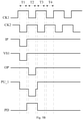
- the embodiment of the present disclosure further provides some other signal time sequence diagrams of the shift register. As shown in Fig. 5B , the implementation mode shown in Fig. 5A is transformed. Only differences between the present embodiment and the embodiment of the shift register shown in Fig. 4a are illustrated below, and similarities are omitted here.
- the first threshold control signal end VS1 uses a signal that is the same as the signal of the input signal end IP.
- the first threshold control signal end VS1 and the input signal end IP may be input into the shift register by using different signal lines.
- the first threshold control signal end VS1 and the input signal end IP may be input into the shift register by using a same signal line, thereby reducing the number of the signal lines.
- the shift register shown in Fig. 4A is exemplified below to describe the working process of the above-mentioned shift register provided by the embodiment of the present disclosure in combination with the signal time sequence diagram shown in Fig. 5B .
- an input phase T1 an output phase T2, a reset phase T3 and a reset holding phase T4 in the signal time sequence diagram as shown in Fig. 5B are selected.
- the switched-on fifth transistor M5 may provide the low-level signal of the first reference signal end VREF1 to the pull-down node PD to enable the signal of the pull-down node PD to be the low-level signal, so as to control the fourth transistor M4 and the seventh transistor M7 to be switched on.
- the switched-on seventh transistor M7 may provide the high-level signal of the second reference signal end VREF2 to the signal output end OP to enable the signal output end OP to output the high-level signal.
- the switched-on second transistor M2 may provide the low-level signal of the input signal end IP to the second pull-up node PU_2 to enable the signal of the second pull-up node PU_2 to be the low-level signal.
- the signal of the first pull-up node PU_1 is the high-level signal, so that an electrode, connected to the first pull-up node PU_1, of the first transistor M1 in the current frame is used as the source.
- the switched-on first transistor M1 switches on the second pull-up node PU_2 and the first pull-up node PU_1, thereby timely enabling the signal of the first pull-up node PU_1 to be the low-level signal to control the eighth transistor M8 to be switched on.
- the switched-on eighth transistor M8 provides the high-level signal of the first clock signal end CK1 to the signal output end OP to enable the signal output end OP to output the high-level signal.
- the switched-on sixth transistor M6 may provide the high-level signal of the second clock signal end CK2 to the pull-down node PD to enable the signal of the pull-down node PD to be the high-level signal, so as to control the fourth transistor M4 and the seventh transistor M7 to be switched off.
- the eighth transistor M8 is switched on under the control of the signal of the first pull-up node PU_1 to provide the high-level signal of the first clock signal end CK1 to the signal output end OP to enable the signal output end OP to output the high-level signal.
- the second transistor M2 and the fifth transistor M5 are both switched off, and then the first pull-up node PU_1 is kept at the low-level signal under the action of the second capacitor C2 to control the eighth transistor M8 to be switched on, thereby providing the low-level signal of the first clock signal end CK1 to the signal output end OP to enable the signal output end OP to output the low-level signal.
- the level of the first pull-up node PU_1 is further pulled down to control the eighth transistor M8 to be completely switched on as much as possible to provide the low-level signal of the first clock signal end CK1 to the signal output end OP, so that the signal output end OP outputs the low-level signal.
- the gate of the first transistor M1 has the voltage of the low-level signal, and the voltage of the source of the first transistor M1 is the voltage of the low-level signal, so that the first transistor M1 may not satisfy V gs1 ⁇ V th1 , and then is switched off as much as possible. Therefore, the level of the first pull-up node PU_1 may be kept stable, and the phenomenon of an unstable output of the signal output end OP due to the rise of the level, caused by leakage, of the first pull-up node PU_1 is avoided.
- the signal of the pull-down node PD may be kept being the high-level signal, thereby controlling the fourth transistor M4 and the seventh transistor M7 to be both switched off and avoiding adverse effect on the signal output by the signal output end OP.
- the gate of the first transistor M1 has the voltage of the low-level signal, and the voltage of the source of the first transistor M1 is the voltage of the high-level signal, so that the first transistor M1 may be enabled to satisfy V gs1 ⁇ V th1 and be switched on, and the second pull-up node PU_2 and the first pull-up node PU_1 are switched on, so as to control the eighth transistor M8 to be switched off.
- the switched-on fifth transistor M5 may provide the low-level signal of the first reference signal end VREF1 to the pull-down node PD to enable the signal of the pull-down node PD to be the low-level signal, so as to control the fourth transistor M4 and the seventh transistor M7 to be switched on.
- the switched-on seventh transistor M7 may provide the high-level signal of the second reference signal end VREF2 to the signal output end OP to enable the signal output end OP to output the high-level signal.
- an electrode, electrically connected to the second pull-up node PU_2, of the first transistor M1 is used as the source.
- V th1 of the first transistor M1 may be enabled to move to left.
- the gate of the first transistor M1 has the voltage of the low-level signal, and the voltage of the source of the first transistor M1 is the voltage of the high-level signal, so that the first transistor M1 may be enabled to satisfy V gs1 ⁇ V th1 and be switched on, and the second pull-up node PU_2 and the first pull-up node PU_1 are switched on, so as to control the eighth transistor M8 to be switched off.
- the switched-on seventh transistor M7 may provide the high-level signal of the second reference signal end VREF2 to the signal output end OP to enable the signal output end OP to output the high-level signal.
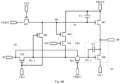
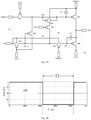
- the embodiment of the present disclosure provides some other shift registers. As shown in Fig. 4B , the implementation mode shown in Fig. 4A is transformed. Only differences between the present embodiment and the embodiment of the shift register shown in Fig. 4A are illustrated below, and similarities are omitted here.
- the second gate of the first transistor M1 may be enabled to be coupled to the first electrode of the second transistor M2, so as to further reduce the usage space of the signal lines.
- the signal time sequence diagram corresponding to the shift register shown in Fig. 4B is as shown in Fig. 5B .
- the working processes of the shift register shown in Fig. 4B may refer to the working processes of the shift register shown in Fig. 4A under the signal time sequence diagram shown in Fig. 5B , and will not be repeatedly described here.
- the second gate of the first transistor M1 may be enabled to be coupled to the gate of the second transistor M2, so as to further reduce the usage space of the signal lines, which is not limited here.
- the signal output by the signal output end OP of the shift register shown in Fig. 4B is simulated, the simulation diagram of which is as shown in Fig. 6 .
- the X-coordinate represents time
- the Y-coordinate represents voltage. It can be known in combination with Fig. 4B , Fig. 5B , and Fig. 6 , at the output phase T2, the signal output end OP may stably output the signal, thereby avoiding the problem of unsteadiness caused by the leakage of the first pull-up node PU_1.
- the embodiment of the present disclosure provides some other shift registers. As shown in Fig. 7 , the implementation mode shown in Fig. 4A is transformed. Only differences between the present embodiment and the embodiment of the shift register shown in Fig. 4A are illustrated below, and similarities are omitted here.
- the input circuit 10 may also include: a double-gate type second transistor M2.
- the first gate of the second transistor M2 is configured to be coupled to the second clock signal end CK2, and the second gate of the second transistor M2 is configured to be coupled to a second threshold control signal end VS2.
- the first electrode of the second transistor M2 is configured to be coupled to the input signal end IP, and the second electrode of the second transistor M2 is coupled to the first electrode (i.e., the second pull-up node PU_2) of the first transistor M1.
- the second threshold control signal end VS2 is configured to receive a signal at least having a level opposite to the level of a signal of the first reference signal end VREF1.
- the level of one part of the signals of the second threshold control signal end VS2 may be opposite to the level of the signal of the first reference signal end VREF1.
- the level of the other part of the signals of the second threshold control signal end VS2 may be the same as the level of the signal of the first reference signal end VREF1.
- the first gate of the second transistor is enabled to be dominated by adjusting the thickness of the gate insulating layer, so that the second transistor M2 is switched on when the relationship between the voltage difference V gs2 between the gate (i.e., the first gate) and the source of the second transistor M2 and the threshold voltage V th2 of the second transistor M2 satisfies the formula: v gs2 ⁇ V th2 .
- the voltage difference represented by V gs2 between the first gate and the source of the second transistor M2 is illustrated below as an example.
- the pull-up control circuit 30 may also include: a third transistor M3 and a double-gate type fourth transistor M4.
- the gate of the third transistor M3 is configured to be coupled to the first clock signal end CK1.
- the first electrode of the third transistor M2 is coupled to the first electrode (i.e., the second pull-up node PU_2) of the first transistor M1.
- the second electrode of the third transistor M3 is coupled to the first electrode of the fourth transistor M4.
- the first gate of the fourth transistor M4 is coupled to the gate (i.e., the pull-down node PD) of the seventh transistor M7.
- the second gate of the fourth transistor M4 is configured to be coupled to a third threshold control signal end VS3.
- the second electrode of the fourth transistor M4 is configured to be coupled to the second reference signal end VREF2.
- the third threshold control signal end VS3 is configured to receive a signal at least having a level opposite to the level of a signal of the first reference signal end VREF1.
- the level of one part of the signals of the third threshold control signal end VS3 may be opposite to the level of the signal of the first reference signal end VREF1.
- the level of the other part of the signals of the third threshold control signal end VS3 may be the same as the level of the signal of the first reference signal end VREF1.
- the first gate of the fourth transistor is enabled to be dominated by adjusting the thickness of the gate insulating layer, so that the fourth transistor M4 is switched on when the relationship between the voltage difference V gs4 between the gate (i.e., the first gate) and the source of the fourth transistor M4 and the threshold voltage V th4 of the fourth transistor M4 satisfies the formula: V gs4 ⁇ V th4 .
- the voltage difference represented by V gs4 between the first gate and the source of the fourth transistor M4 is illustrated below as an example.
- the shift register shown in Fig. 7 is exemplified below to describe the working process of the above-mentioned shift register provided by the embodiment of the present disclosure in combination with the signal time sequence diagram shown in Fig. 8 .
- an input phase T1 an output phase T2, a reset phase T3 and a reset holding phase T4 in the signal time sequence diagram as shown in Fig. 8 are selected.
- the switched-on seventh transistor M7 may provide the high-level signal of the second reference signal end VREF2 to the signal output end OP to enable the signal output end OP to output the high-level signal.
- the threshold voltage V th2 of the second transistor M2 may be enabled to move to right, thereby enabling the second transistor M2 to be completely switched on as much as possible, so as to accelerate a charge process of providing the low-level signal of the input signal end IP to the second pull-up node PU_2 to enable the signal of the second pull-up node PU_2 to be the low-level signal as soon as possible.
- the sixth transistor M6 is switched on under the control of the signal of the second pull-up node PU_2 to provide the low-level signal of the second clock signal end CK2 to the pull-down node PD, so as to enable the signal of the pull-down node PD to be the low-level signal.
- V th1 of the first transistor M1 may be enabled to move to right, so that the first transistor M1 satisfies V gs1 ⁇ V th1 , and then is completely switched on as much as possible.
- the switched-on first transistor M1 switches on the second pull-up node PU_2 and the first pull-up node PU_1, thereby timely enabling the signal of the first pull-up node PU_1 to be the low-level signal to control the eighth transistor M8 to be switched on.
- the switched-on eighth transistor M8 provides the high-level signal of the first clock signal end CK1 to the signal output end OP to enable the signal output end OP to output the high-level signal.
- the first pull-up node PU_1 is kept at the low-level signal under the action of the second capacitor C2.
- the signal of the second pull-up node PU_2 may be enabled to be the low-level signal, so as to control the sixth transistor M6 to be switched on.
- the switched-on sixth transistor M6 may provide the high-level signal of the second clock signal end CK2 to the pull-down node PD to enable the signal of the pull-down node PD to be the high-level signal, so as to control the fourth transistor M4 and the seventh transistor M7 to be switched off.
- the eighth transistor M8 is switched on under the control of the signal of the first pull-up node PU_1 to provide the high-level signal of the first clock signal end CK1 to the signal output end OP to enable the signal output end OP to output the high-level signal.
- the first pull-up node PU_1 is kept at the low-level signal under the action of the second capacitor C2 to control the eighth transistor M8 to be switched on, thereby providing the low-level signal of the first clock signal end CK1 to the signal output end OP to enable the signal output end OP to output the low-level signal.
- the level of the first pull-up node PU_1 is further pulled down to control the eighth transistor M8 to be completely switched on as much as possible to provide the low-level signal of the first clock signal end CK1 to the signal output end OP, so that the signal output end OP outputs the low-level signal.
- the gate of the first transistor M1 has the voltage of the low-level signal, and the voltage of the source of the first transistor M1 is the voltage of the low-level signal, so that the first transistor M1 may not satisfy V gs1 ⁇ V th1 , and then is switched off.
- the threshold voltage of the fourth transistor M4 may be enabled to move to left, and the fourth transistor M4 may be completely switched off as much as possible, so as to avoid the influence, caused by the leakage of the fourth transistor M4, on the second pull-up node PU_2 and prolong the holding time of the low-level signal of the second pull-up node PU_2.
- the sixth transistor M6 provides the high-level signal of the second clock signal end CK2 to the pull-down node PD under the control of the signal of the second pull-up node PU_2, so as to control the seventh transistor M7 to be switched off and avoid the adverse effect on the signal output by the signal output end OP.
- the gate of the first transistor M1 has the voltage of the low-level signal, and the voltage of the source of the first transistor M1 is the voltage of the high-level signal, so that the first transistor M1 may be enabled to satisfy V gs1 ⁇ V th1 and be switched on, and the second pull-up node PU_2 and the first pull-up node PU_1 are switched on, so as to control the eighth transistor M8 to be switched off.
- the switched-on fifth transistor M5 provides the low-level signal of the first reference signal end VREF1 to the pull-down node PD to enable the signal of the pull-down node PD to be the low-level signal, so as to control the seventh transistor M7 to be switched on.
- the second transistor M2 and the fifth transistor M5 are both switched off, and then the signal of the pull-down node PD is kept being the low-level signal under the action of the first capacitor C1 to control the seventh transistor M7 to be switched on, thereby providing the high-level signal of the second reference signal end VREF2 to the signal output end OP to enable the signal output end OP to output the high-level signal.
- the gate of the first transistor M1 has the voltage of the low-level signal, and the voltage of the source of the first transistor M1 is the voltage of the high-level signal, so that the first transistor M1 may be enabled to satisfy V gs1 ⁇ V th1 and be switched on, and the second pull-up node PU_2 and the first pull-up node PU_1 are switched on, so as to control the eighth transistor M8 to be switched off.
- the embodiment of the present disclosure provides some other shift registers. As shown in Fig. 9A , the implementation mode shown in Fig. 7 is transformed. Only differences between the present embodiment and the embodiment of the shift register shown in Fig. 7 are illustrated below, and similarities are omitted here.
- the second gate of the first transistor M1 may be enabled to be coupled to the first electrode of the second transistor M2.
- the first threshold control signal end and the input signal end may be configured to receive a same signal. That is, the second gate of the first transistor M1 receives the signal of the input signal end IP, so as to further reduce the usage space of the signal lines. In this way, a same signal line may be used to input the signal to the first threshold control signal end and the input signal end.
- the second gate of the second transistor M2 may be enabled to be coupled to the first electrode of the second transistor M2.
- the second threshold control signal end and the input signal end may be configured to receive a same signal. That is, the second gate of the second transistor M2 receives the signal of the input signal end IP, so as to further reduce the usage space of the signal lines. In this way, a same signal line may be used to input the signal to the second threshold control signal end and the input signal end.
- the first threshold control signal end and the second threshold control signal end may be configured to receive a same signal.
- the second gate of the first transistor M1 may be enabled to be coupled to the second gate of the second transistor M2, so as to both receive the signal of the input signal end IP.
- the signal of the third threshold control signal end and the signal of the pull-down node may be set as a same signal.
- the second gate of the fourth transistor M4 may be enabled to be coupled to the gate (i.e., the pull-down node PD) of the seventh transistor M7.
- the working process of the shift register shown in Fig. 9A may refer to the working process of the shift register shown in Fig. 7 , and will not be repeatedly described here.
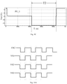
- the signal output by the signal output end OP and the signal of the first pull-up node PU_1 of the shift register shown in Fig. 9A are simulated, as shown in Fig. 9B and Fig. 9C .
- the X-coordinate represents time
- the Y-coordinate represents voltage. It can be known in combination with Fig. 9A to Fig. 9C , at the output phase T2, the signal output end OP may stably output the signal, thereby avoiding the problem of unsteadiness caused by the leakage of the first pull-up node PU_1.
- the embodiment of the present disclosure provides signal time sequence diagrams of some shift registers. As shown in Fig. 10A and Fig. 10B , the implementation mode shown in Fig. 8 is transformed. Only differences between the present embodiment and the embodiment of the shift register shown in Fig. 8 are illustrated below, and similarities are omitted here.
- the first threshold control signal end VS1 may be configured to be a clock signal.
- the second threshold control signal end VS2 may be configured to be a clock signal.
- the third threshold control signal end VS3 may be configured to be a clock signal.
- the first threshold control signal end VS1 and the second threshold control signal end VS2 may be configured to receive a same signal.
- the first threshold control signal end VS1 and the third threshold control signal end VS3 may be configured to receive a same signal.
- the first threshold control signal end VS1, the second threshold control signal end VS2, and the third threshold control signal end VS3 may be configured to receive a same signal. In this way, a same signal line may be used to input the clock signal to the first threshold control signal end VS1, the second threshold control signal end VS2, and the third threshold control signal end VS3.
- the shift register shown in Fig. 7 is exemplified below to describe the working process of the above-mentioned shift register provided by the embodiment of the present disclosure in combination with the signal time sequence diagrams shown in Fig. 10B .
- an input phase T1 an output phase T2, a reset phase T3 and a reset holding phase T4 in the signal time sequence diagram as shown in Fig. 10B are selected.
- the working process of this phase may refer to the working process of the shift register shown in Fig. 7 at the input phase T1, and will not be repeatedly described here.
- the working process may also refer to the working process of the shift register shown in Fig. 7 after the input phase T1 and before the output phase T2, and will not be repeatedly described here.
- the working process of this phase may refer to the working process of the shift register shown in Fig. 7 at the output phase T2, and will not be repeatedly described here.
- the threshold voltage V th2 of the second transistor M2 may be enabled to move to right, thereby enabling the second transistor M2 to be completely switched on as much as possible, so as to accelerate a charge process of providing the high-level signal of the input signal end IP to the second pull-up node PU_2 to enable the signal of the second pull-up node PU_2 to be the high-level signal as soon as possible.
- the first transistor M1 may be timely switched on to provide the high-level signal of the second pull-up node PU_2 to the first pull-up node PU_1, so as to control the eighth transistor M8 to be switched off.
- the rest working process of this phase may refer to the working process of the shift register shown in Fig. 7 at the reset phase T3, and will not be repeatedly described here.
- the rest working process of this phase may refer to the working process of the shift register shown in Fig. 7 at the reset holding phase T4, and will not be repeatedly described here.
- the embodiment of the present disclosure provides signal time sequence diagrams of some shift registers. As shown in Fig. 10C , the implementation mode shown in Fig. 8 is transformed. Only differences between the present embodiment and the embodiment of the shift register shown in Fig. 8 are illustrated below, and similarities are omitted here.
- the first threshold control signal end VS1 may be configured to be a clock signal which is the same as the time sequence of the second clock signal end CK2. In this way, the time sequence of the second clock signal end CK2 may be used to input the clock signal to the first threshold control signal end VS1.
- the second threshold control signal end VS2 may be configured to be a clock signal which is the same as the time sequence of the second clock signal end CK2. In this way, the time sequence of the second clock signal end CK2 may be used to input the clock signal to the second threshold control signal end VS2.
- the third threshold control signal end VS3 may be configured to be a clock signal which is the same as the time sequence of the second clock signal end CK2. In this way, the time sequence of the second clock signal end CK2 may be used to input the clock signal to the third threshold control signal end VS3.
- the working process of the shift register shown in Fig. 8 under the signal time sequence diagram shown in Fig. 10C may refer to the working process of the shift register shown in Fig. 8 under the signal time sequence diagram shown in Fig. 10B , and will not be repeatedly described here.
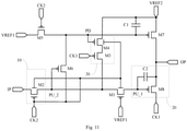
- the embodiment of the present disclosure provides some other shift registers. As shown in Fig. 11 , the implementation mode shown in Fig. 7 is transformed. Only differences between the present embodiment and the embodiment of the shift register shown in Fig. 7 are illustrated below, and similarities are omitted here.
- the first threshold control signal end and the second clock signal end may be set as a same clock signal.
- the first threshold control signal end is the second clock signal end CK2.
- the second gate of the first transistor M1 is coupled to the first gate of the second transistor M2 to enable the second gate of the first transistor M1 to receive the signal of the second clock signal end CK2. In this way, a same signal line may be used to input the signal to the first threshold control signal end and the second clock signal end.
- the second threshold control signal end and the second clock signal end may be set as a same clock signal.
- the second threshold control signal end is the second clock signal end CK2.
- the second gate of the second transistor M2 is coupled to the first gate of the second transistor M2 to enable the second gate of the second transistor M2 to receive the signal of the second clock signal end CK2. In this way, a same signal line may be used to input the signal to the first threshold control signal end and the second clock signal end.
- the third threshold control signal end and the second clock signal end may be set as a same clock signal.
- the second gate of the fourth transistor M4 may be coupled to the gate of the fifth transistor M5.
- the second gate of the fourth transistor M4 may also be coupled to the first gate of the second transistor M2, so as to enable the second gate of the fourth transistor M4 to receive the signal of the second clock signal end CK2. In this way, a same signal line may be used to input the signal to the first threshold control signal end and the second clock signal end.
- the shift register shown in Fig. 11 is exemplified below to describe the working process of the above-mentioned shift register provided by the embodiment of the present disclosure in combination with the signal time sequence diagram shown in Fig. 12 .
- the working process of this phase may refer to the working process of the shift register shown in Fig. 7 at the input phase T1, and will not be repeatedly described here.
- the working process after the input phase T1 and before the output phase T2 may also refer to the working process of the shift register shown in Fig. 7 after the input phase T1 and before the output phase T2, and will not be repeatedly described here.
- the working process of this phase may refer to the working process of the shift register shown in Fig. 7 at the output phase T2, and will not be repeatedly described here.
- the second transistor M2 may be completely switched on as much as possible to timely provide the high-level signal of the input signal end IP to the second pull-up node PU_2 to enable the signal of the second pull-up node PU_2 to be the high-level signal, so as to control the sixth transistor M6 to be switched off.
- the first transistor M1 may be timely switched on to provide the high-level signal of the second pull-up node PU_2 to the first pull-up node PU_1 to enable the signal of the first pull-up node PU_1 to be the high-level signal, so as to timely control the eighth transistor M8 to be switched off.
- the rest working process of this phase may refer to the working process of the shift register shown in Fig. 7 at the reset phase T3, and will not be repeatedly described here.
- the rest working process of this phase may refer to the working process of the shift register shown in Fig. 7 at the reset holding phase T4, and will not be repeatedly described here.
- the embodiment of the present disclosure provides some other shift registers. As shown in Fig. 13 , the implementation mode shown in Fig. 11 is transformed. Only differences between the present embodiment and the embodiment of the shift register shown in Fig. 11 are illustrated below, and similarities are omitted here.
- the signal of the third threshold control signal end and the signal of the pull-down node may be a same signal.
- the second gate of the fourth transistor M4 may be coupled to the gate (i.e., the pull-down node PD) of the seventh transistor M7.
- the shift register shown in Fig. 13 is exemplified below to describe the working process of the above-mentioned shift register provided by the embodiment of the present disclosure in combination with the signal time sequence diagram shown in Fig. 12 .
- an input phase T1 an output phase T2, a reset phase T3 and a reset holding phase T4 in the signal time sequence diagram as shown in Fig. 12 are selected.
- the working process of this phase may refer to the working process of the shift register shown in Fig. 7 at the input phase T1, and will not be repeatedly described here.
- the working process after the input phase T1 and before the output phase T2 may also refer to the working process of the shift register shown in Fig. 7 after the input phase T1 and before the output phase T2, and will not be repeatedly described here.
- the working process of this phase may refer to the working process of the shift register shown in Fig. 7 at the output phase T2, and will not be repeatedly described here.
- the second transistor M2 may be completely switched on as much as possible to timely provide the high-level signal of the input signal end IP to the second pull-up node PU_2 to enable the signal of the second pull-up node PU_2 to be the high-level signal, so as to control the sixth transistor M6 to be switched off.
- the first transistor M1 may be timely switched on to provide the high-level signal of the second pull-up node PU_2 to the first pull-up node PU_1 to enable the signal of the first pull-up node PU_1 to be the high-level signal, so as to timely control the eighth transistor M8 to be switched off.
- the rest working process of this phase may refer to the working process of the shift register shown in Fig. 7 at the reset phase T3, and will not be repeatedly described here.
- the embodiment of the present disclosure provides some other shift registers. As shown in Fig. 14A , the implementation mode of the signal time sequence diagram shown in Fig. 8 is transformed. Only differences between the present embodiment and the signal time sequence diagram shown in Fig. 8 are illustrated below, and similarities are omitted here.
- the first threshold control signal end VS1 is configured to receive a fixed voltage signal.
- the first threshold control signal end VS1 is configured to receive a direct current fixed voltage signal having a first voltage value, so as to ensure that the first transistor M1 may be completely switched off as much as possible at the output phase T2 to reduce the leakage influence, caused by leakage current, on the first pull-up node PU_1.
- the first threshold control signal end VS1 may be configured to receive a high-level fixed voltage signal.
- a first voltage value may be set according to actual application.
- the first voltage value when the display device uses a relatively low refresh frequency, since the shift register works at a relatively low refresh frequency (such as 1 Hz) or is in a holding state, the first voltage value may be set to be a high voltage, so as to reduce the leakage and ensure the output stability of the shift register. Therefore, the shift register may not work abnormally.
- the first voltage value when the display device uses a relatively high refresh frequency, since the shift register works at a relatively high refresh frequency (such as 60 Hz and 120 Hz), the first voltage value may be set to be 0 V or a negative voltage to ensure a response speed of the shift register.
- the above first voltage value may be designed and determined according to an actual application environment, and is not limited here.
- the first threshold control signal end VS1 may be configured to receive a low-level fixed voltage signal. Further, when the display device uses different refresh frequencies, the first voltage value may be set according to actual applications, and is not limited here.
- the second threshold control signal end VS2 is configured to receive a fixed voltage signal.
- the second threshold control signal end VS2 is configured to receive a direct current fixed voltage signal having a second voltage value, so as to ensure that the second transistor M2 may be completely switched off as much as possible at the output phase T2 to reduce the leakage influence, caused by leakage current, on the second pull-up node PU_2.
- the second transistor M2 is the P-type transistor
- the second threshold control signal end VS2 may be configured to receive a high-level fixed voltage signal.
- a second voltage value may be set according to actual application.
- the second voltage value may be set to be a high voltage, so as to reduce the leakage and ensure the output stability of the shift register. Therefore, the shift register may not work abnormally.
- the second voltage value may be set to be 0 V or a negative voltage to ensure a response speed of the shift register.
- the above second voltage value may be designed and determined according to an actual application environment, and is not limited here.
- the second threshold control signal end VS2 may be configured to receive a low-level fixed voltage signal.
- the second voltage value may be set according to actual applications, and is not limited here.
- the third threshold control signal end VS3 may also be configured to receive a fixed voltage signal.
- the third threshold control signal end VS3 is configured to receive a direct current fixed voltage signal having a third voltage value, so as to ensure that the fourth transistor M4 may be completely switched off as much as possible at the output phase T2 to reduce the leakage influence, caused by leakage current, on the second pull-up node PU_2.
- the fourth transistor M4 is the P-type transistor
- the third threshold control signal end VS3 may be configured to receive a high-level fixed voltage signal.
- a third voltage value may be set according to actual application.
- the third voltage value may be set to be a high voltage, so as to reduce the leakage and ensure the output stability of the shift register. Therefore, the shift register may not work abnormally.
- the third voltage value may be set to be 0 V or a negative voltage to ensure a response speed of the shift register.
- the above third voltage value may be designed and determined according to an actual application environment, and is not limited here.
- the third threshold control signal end VS3 may be configured to receive a low-level fixed voltage signal. Further, when the display device uses different refresh frequencies, the third voltage value may be set according to actual applications, and is not limited here.
- the second threshold control signal end VS2 and the first threshold control signal end VS1 may be configured to receive a same signal.
- the second gate of the first transistor M1 and the second gate of the second transistor M2 are coupled to both receive the signal of the first threshold control signal end VS1, so that one signal line is used to input the signal to the second gate of the first transistor M1 and the second gate of the second transistor M2.
- the third threshold control signal end VS3 and the first threshold control signal end VS1 may also be configured to receive a same signal.
- the second gate of the first transistor M1 and the second gate of the fourth transistor M4 are coupled to both receive the signal of the first threshold control signal end VS1, so that one signal line is used to input the signal to the second gate of the first transistor M1 and the second gate of the fourth transistor M4.
- the third threshold control signal end VS3, the second threshold control signal end VS2, and the first threshold control signal end VS1 may also be configured to receive a same signal.
- the second gate of the first transistor M1, the second gate of the second transistor M2, and the second gate of the fourth transistor M4 are coupled to receive the signal of the first threshold control signal end VS1, so that one signal line is used to input the signal to the second gate of the first transistor M1, the second gate of the second transistor M2, and the second gate of the fourth transistor M4.
- the shift register shown in Fig. 14A is exemplified below to describe the working process of the above-mentioned shift register provided by the embodiment of the present disclosure in combination with the signal time sequence diagram shown in Fig. 14b .
- an input phase T1 an output phase T2, a reset phase T3 and a reset holding phase T4 in the signal time sequence diagrams as shown in Fig. 14B are selected.
- the switched-on seventh transistor M7 provides the high-level signal of the second reference signal end VREF2 to the signal output end OP to make the signal output end OP to output the high-level signal.
- the working process of this phase may refer to the working process in Fig. 8 at the input phase T1, and will not be repeatedly described here.
- the working process after the input phase T1 and before the output phase T2 may also refer to the working process in Fig. 88 after the input phase T1 and before the output phase T2, and will not be repeatedly described here.
- the working process of this phase may refer to the working process in Fig. 8 at the output phase T2, and will not be repeatedly described here.
- the rest working process of this phase may refer to the working process in Fig. 8 at the reset holding phase T4, and will not be repeatedly described here.
- the embodiment of the present disclosure further provides a driving method of the above-mentioned shift register.
- the driving method may include the following phases.
- the input circuit controls the level of the signal of the first electrode of the first transistor according to the signals of the input signal end and the second clock signal end; the first transistor is switched on; the output circuit provides the signal of the first clock signal to the signal output end in response to the signal of the second electrode of the first transistor.
- a threshold voltage of the first transistor moves in response to the signal of the first threshold control signal end; the first transistor is switched off; the output circuit provides the signal of the first clock signal end to the signal output end in response to the signal of the second electrode of the first transistor, where the level of the signal of the first threshold control signal end is opposite to the level of the signal of the first reference signal end.
- a threshold voltage of the second transistor moves in response to the signal of the second threshold control signal end, and the second transistor is switched off; and a threshold voltage of the fourth transistor moves in response to the signal of the third threshold control signal end, and the fourth transistor is switched off.
- the input phase in S100 may further include that: the fifth transistor provides the signal of the first reference signal end to the gate of the seventh transistor in response to the signal of the second clock signal end; the sixth transistor provides the signal of the second clock signal end to the gate of the seventh transistor in response to the signal of the first electrode of the first transistor; and the seventh transistor provides the signal of the second reference signal end to the signal output end in response to the signal of the gate of the seventh transistor.
- the driving method may further include the following phase.
- the input circuit controls the level of the signal of the first electrode of the first transistor according to the signals of the input signal end and the second clock signal end; the first transistor switches on the input circuit and the output circuit; the fifth transistor provides the signal of the first reference signal end to the gate of the seventh transistor in response to the signal of the second clock signal end; and the seventh transistor provides the signal of the second reference signal end to the signal output end in response to the signal of the gate of the seventh transistor.
- the driving method may further include that: at a reset holding phase, the first capacitor maintains the signal of the gate of the seventh transistor; the seventh transistor provides the signal of the second reference signal end to the signal output end in response to the signal of the gate of the seventh transistor; and the pull-up control circuit provides the signal of the second reference signal end to the second pull-up node in response to the signals of the first clock signal end and the gate of the seventh transistor.
- the driving principle and the specific implementation mode of the driving method are the same as the principle and the implementation mode of the shift register of the above embodiment, so that the driving method may be implemented by referring to the specific implementation mode of the shift register in the above embodiment, and will not be repeatedly described.
- the embodiment of the present disclosure further provides a gate driving circuit.
- the gate driving circuit includes a plurality of the above-mentioned shift registers SR(1), SR(2)...SR(n-1), SR(n)...SR(N-1), SR(N) (totally N shift registers, 1 ⁇ n ⁇ N) that are cascaded.
- the input signal end IP of the first stage of shift register SR(1) is configured to be coupled to a frame trigger signal end STV.
- the input signal end IP of the next stage of shift register SR(n) is configured to be coupled to the signal output end OP of the previous stage of shift register SR(n-1).
- each shift register in the gate driving circuit is the same as the above shift register of the present disclosure in function and structure, and repeated parts are not described.
- the gate driving circuit may be set in a liquid crystal display panel, or may be set in an electroluminescence display panel, and is not limited here.
- the first reference signal ends VREF1 of the various stages of shift registers SR(n) are all coupled to a same direct current signal end vdd
- the second reference signal ends VREF2 of the various stages of shift registers SR(n) are all coupled to a same direct current signal end vss.
- the first clock signal end CK1 of the (2k-1)th stage of shift register and the second clock signal end CK2 of the 2kth stage of shift register are both coupled to a same clock end, i.e., a first clock end ck1.
- the second clock signal end CK2 of the (2k-1)th stage of shift register and the first clock signal end CK1 of the 2kth stage of shift register are both coupled to a same clock end, i.e., a second clock end ck2, where k is a positive integer.
- the first threshold control signal end of the (2k-1)th stage of shift register and the first threshold control signal end of the 2kth stage of shift register are both coupled to a same clock end, i.e., a third clock end ck3
- the first threshold control signal end of the (2k-1)th stage of shift register and the first threshold control signal end of the 2kth stage of shift register are both coupled to a same clock end, i.e., a fourth clock end ck4.
- the third threshold control signal end of the (2k-1)th stage of shift register and the third threshold control signal end of the 2kth stage of shift register are both coupled to a same clock end, i.e., a fifth clock end ck5
- the third threshold control signal end of the (2k-1)th stage of shift register and the third threshold control signal end of the 2kth stage of shift register are both coupled to a same clock end, i.e., a sixth clock end ck6.
- the embodiment of the present disclosure further provides a display device, including the above-mentioned gate driving circuit provided by the embodiment of the present disclosure.
- the principle of the display device for solving problems is similar to that of the shift register, so that the implementation of the display device may refer to the implementation of the foregoing shift register, and repeated parts are omitted.
- the display device provided by the embodiment of the present disclosure may be a mobile phone as shown in Fig. 17 .
- the display device provided by the embodiment of the present disclosure may be any product or component having a display function, such as a tablet computer, a television, a display, a notebook computer, a digital photo frame, and a navigator.
- a display function such as a tablet computer, a television, a display, a notebook computer, a digital photo frame, and a navigator.
- Other indispensable components of the display device are all understood by those skilled in the art, and are not described herein and should not be construed as limiting the present disclosure.
- the first transistor is set as the double-gate type transistor.
- the first gate of the first transistor receives the first reference signal end, and the second gate of the first transistor receives the first threshold control signal end, so that the first transistor may be switched on at the input phase, the reset phase, and the reset holding phase.
- the signal of the first threshold control signal end controls a threshold voltage V th1 of the first transistor to enable the threshold voltage V th1 of the first transistor to move, so as to enable the first transistor to be switched off as much as possible at the output phase, which may keep the level of the signal of the first pull-up node to be stabilized and avoid the influence of leakage on the signal of the first pull-up node. Therefore, the stability of the signal output by the signal output end is improved. Then, the shift register is favorably applied to the low-frequency driven display device, and is conductive to reducing the power consumption.
Landscapes
- Engineering & Computer Science (AREA)
- Physics & Mathematics (AREA)
- Computer Hardware Design (AREA)
- General Physics & Mathematics (AREA)
- Theoretical Computer Science (AREA)
- Shift Register Type Memory (AREA)
- Control Of Indicators Other Than Cathode Ray Tubes (AREA)
- Liquid Crystal Display Device Control (AREA)
Applications Claiming Priority (1)
| Application Number | Priority Date | Filing Date | Title |
|---|---|---|---|
| PCT/CN2019/079589 WO2020191597A1 (fr) | 2019-03-25 | 2019-03-25 | Registre à décalage et son procédé d'attaque, circuit d'attaque de grille, et dispositif d'affichage |
Publications (3)
| Publication Number | Publication Date |
|---|---|
| EP3951765A1 true EP3951765A1 (fr) | 2022-02-09 |
| EP3951765A4 EP3951765A4 (fr) | 2022-11-16 |
| EP3951765B1 EP3951765B1 (fr) | 2024-01-24 |
Family
ID=72610741
Family Applications (1)
| Application Number | Title | Priority Date | Filing Date |
|---|---|---|---|
| EP19861299.6A Active EP3951765B1 (fr) | 2019-03-25 | 2019-03-25 | Registre à décalage, circuit d'attaque de grille, et dispositif d'affichage |
Country Status (4)
| Country | Link |
|---|---|
| US (1) | US11170682B2 (fr) |
| EP (1) | EP3951765B1 (fr) |
| CN (1) | CN112041920A (fr) |
| WO (1) | WO2020191597A1 (fr) |
Families Citing this family (8)
| Publication number | Priority date | Publication date | Assignee | Title |
|---|---|---|---|---|
| CN109584799A (zh) * | 2019-02-02 | 2019-04-05 | 京东方科技集团股份有限公司 | 一种像素驱动电路、像素电路、显示面板和显示装置 |
| US11462149B2 (en) * | 2020-04-24 | 2022-10-04 | Beijing Boe Technology Development Co., Ltd. | Shift register unit and method for driving the same, gate driving circuit and display device |
| WO2022134111A1 (fr) * | 2020-12-26 | 2022-06-30 | 京东方科技集团股份有限公司 | Registre à décalage et son procédé d'attaque, circuit d'attaque de grille et dispositif d'affichage |
| EP4123634B1 (fr) * | 2021-03-24 | 2025-05-14 | BOE Technology Group Co., Ltd. | Substrat d'affichage et dispositif d'affichage |
| CN115909978B (zh) * | 2021-09-30 | 2024-08-06 | 乐金显示有限公司 | 栅极驱动电路以及包括栅极驱动电路的显示装置 |
| CN119207311A (zh) * | 2023-06-27 | 2024-12-27 | 武汉华星光电半导体显示技术有限公司 | 栅极驱动电路及显示面板 |
| CN116704958B (zh) * | 2023-06-27 | 2025-12-16 | 合肥京东方卓印科技有限公司 | 移位寄存器单元、栅极驱动电路、驱动方法及显示装置 |
| KR20250046457A (ko) * | 2023-09-26 | 2025-04-03 | 삼성디스플레이 주식회사 | 게이트 구동부 및 이를 포함하는 표시 장치 |
Family Cites Families (25)
| Publication number | Priority date | Publication date | Assignee | Title |
|---|---|---|---|---|
| JP5188382B2 (ja) * | 2008-12-25 | 2013-04-24 | 三菱電機株式会社 | シフトレジスタ回路 |
| JP2014167841A (ja) * | 2013-02-28 | 2014-09-11 | Kyocera Corp | シフトレジスタ回路および画像表示装置 |
| KR102041872B1 (ko) * | 2013-05-03 | 2019-11-07 | 엘지디스플레이 주식회사 | 쉬프트 레지스터 및 이를 이용한 평판표시장치 |
| CN103490748B (zh) * | 2013-06-21 | 2015-12-23 | 北京大学深圳研究生院 | 一种锁存器电路单元及用于显示装置的数据驱动电路 |
| KR102050581B1 (ko) * | 2013-06-21 | 2019-12-02 | 삼성디스플레이 주식회사 | 스테이지 회로 및 이를 이용한 유기전계발광 표시장치 |
| KR102085152B1 (ko) * | 2013-07-24 | 2020-03-06 | 삼성디스플레이 주식회사 | 게이트 구동회로 및 이를 포함하는 표시 장치 |
| CN104021769B (zh) * | 2014-05-30 | 2016-06-15 | 京东方科技集团股份有限公司 | 一种移位寄存器、栅线集成驱动电路及显示屏 |
| KR102238636B1 (ko) * | 2014-08-05 | 2021-04-12 | 엘지디스플레이 주식회사 | 표시장치 |
| CN104217693A (zh) * | 2014-09-04 | 2014-12-17 | 京东方科技集团股份有限公司 | 移位寄存器、栅极驱动电路及其驱动方法、显示装置 |
| CN104835442B (zh) * | 2015-05-28 | 2017-09-26 | 京东方科技集团股份有限公司 | 移位寄存器及其驱动方法、栅极驱动电路和显示装置 |
| CN105139795B (zh) * | 2015-09-22 | 2018-07-17 | 上海天马有机发光显示技术有限公司 | 一种栅极扫描电路及其驱动方法、栅极扫描级联电路 |
| US10297331B2 (en) * | 2015-10-30 | 2019-05-21 | Semiconductor Energy Laboratory Co., Ltd. | Semiconductor device and electronic device |
| CN105374331B (zh) * | 2015-12-01 | 2017-11-17 | 武汉华星光电技术有限公司 | 栅极驱动电路和使用栅极驱动电路的显示器 |
| CN105654905B (zh) * | 2016-03-30 | 2018-01-26 | 京东方科技集团股份有限公司 | 移位寄存器及其驱动方法、驱动电路和显示装置 |
| KR102536161B1 (ko) * | 2016-03-31 | 2023-05-25 | 삼성디스플레이 주식회사 | 디스플레이 장치의 스캔 드라이버 및 이를 포함하는 디스플레이 장치 |
| CN106782663B (zh) * | 2017-01-12 | 2019-12-17 | 上海天马有机发光显示技术有限公司 | 一种移位寄存器及栅极驱动电路 |
| CN108573667B (zh) * | 2017-03-09 | 2019-11-15 | 合肥鑫晟光电科技有限公司 | 移位寄存器单元及其驱动方法、栅极驱动电路和显示装置 |
| CN107039014B (zh) * | 2017-05-26 | 2019-03-05 | 京东方科技集团股份有限公司 | 移位寄存器单元、其驱动方法、栅极驱动电路及显示面板 |
| CN107093414B (zh) * | 2017-07-03 | 2019-04-30 | 京东方科技集团股份有限公司 | 一种移位寄存器、其驱动方法、栅极驱动电路及显示装置 |
| CN207489450U (zh) * | 2017-12-08 | 2018-06-12 | 京东方科技集团股份有限公司 | 移位寄存器单元、栅极驱动电路、显示装置 |
| CN107784977B (zh) * | 2017-12-11 | 2023-12-08 | 京东方科技集团股份有限公司 | 移位寄存器单元及其驱动方法、栅极驱动电路、显示装置 |
| CN108257567A (zh) * | 2018-01-31 | 2018-07-06 | 京东方科技集团股份有限公司 | Goa单元及其驱动方法、goa电路、触控显示装置 |
| CN208141796U (zh) * | 2018-04-28 | 2018-11-23 | 京东方科技集团股份有限公司 | 移位寄存器单元、栅极驱动电路及显示装置 |
| CN108777129B (zh) * | 2018-06-05 | 2020-07-07 | 京东方科技集团股份有限公司 | 移位寄存器电路及显示装置 |
| CN108831385B (zh) * | 2018-06-25 | 2020-04-28 | 上海天马有机发光显示技术有限公司 | 扫描驱动电路、显示装置和驱动方法 |
-
2019
- 2019-03-25 EP EP19861299.6A patent/EP3951765B1/fr active Active
- 2019-03-25 US US16/651,816 patent/US11170682B2/en active Active
- 2019-03-25 CN CN201980000375.9A patent/CN112041920A/zh active Pending
- 2019-03-25 WO PCT/CN2019/079589 patent/WO2020191597A1/fr not_active Ceased
Also Published As
| Publication number | Publication date |
|---|---|
| CN112041920A (zh) | 2020-12-04 |
| WO2020191597A1 (fr) | 2020-10-01 |
| US11170682B2 (en) | 2021-11-09 |
| EP3951765B1 (fr) | 2024-01-24 |
| EP3951765A4 (fr) | 2022-11-16 |
| US20210020090A1 (en) | 2021-01-21 |
Similar Documents
| Publication | Publication Date | Title |
|---|---|---|
| EP3951765B1 (fr) | Registre à décalage, circuit d'attaque de grille, et dispositif d'affichage | |
| US10685616B2 (en) | Shift register circuit, method for driving the same, gate drive circuit, and display panel | |
| US11189243B2 (en) | Shift register unit, driving method thereof, gate driving circuit and display device | |
| US11276364B2 (en) | Shift register, driving method thereof, driving control circuit and display device | |
| US11468820B2 (en) | Control circuit configuration for shift register unit, gate driving circuit and display device, and method for driving the shift register unit | |
| CN107093414B (zh) | 一种移位寄存器、其驱动方法、栅极驱动电路及显示装置 | |
| CN115668350B (zh) | 移位寄存器、驱动方法、栅极驱动电路及显示装置 | |
| US11170696B2 (en) | Gate drive circuit and display panel | |
| CN109448656B (zh) | 移位暂存器和栅极驱动电路 | |
| US11854508B2 (en) | Driving method and device for shift register | |
| US12340866B2 (en) | Shift register unit, driving method thereof, and device | |
| CN103915074A (zh) | 一种移位寄存器单元、栅极驱动装置和显示面板 | |
| CN106910452A (zh) | 移位寄存器单元、其驱动方法、栅极驱动电路及显示装置 | |
| US11710435B2 (en) | Shift register unit and driving method thereof, gate driving circuit, and display device | |
| CN109859701B (zh) | 移位暂存器和栅极驱动电路 | |
| US11328785B2 (en) | Shift register, gate driving circuit and gate driving method | |
| KR102235950B1 (ko) | 시프트 레지스터, 게이트 구동 회로 및 디스플레이 디바이스 | |
| US12548532B2 (en) | Driving circuit and driving method for the same, and display device |
Legal Events
| Date | Code | Title | Description |
|---|---|---|---|
| STAA | Information on the status of an ep patent application or granted ep patent |
Free format text: STATUS: UNKNOWN |
|
| STAA | Information on the status of an ep patent application or granted ep patent |
Free format text: STATUS: THE INTERNATIONAL PUBLICATION HAS BEEN MADE |
|
| PUAI | Public reference made under article 153(3) epc to a published international application that has entered the european phase |
Free format text: ORIGINAL CODE: 0009012 |
|
| STAA | Information on the status of an ep patent application or granted ep patent |
Free format text: STATUS: REQUEST FOR EXAMINATION WAS MADE |
|
| 17P | Request for examination filed |
Effective date: 20200327 |
|
| AK | Designated contracting states |
Kind code of ref document: A1 Designated state(s): AL AT BE BG CH CY CZ DE DK EE ES FI FR GB GR HR HU IE IS IT LI LT LU LV MC MK MT NL NO PL PT RO RS SE SI SK SM TR |
|
| DAV | Request for validation of the european patent (deleted) | ||
| DAX | Request for extension of the european patent (deleted) | ||
| A4 | Supplementary search report drawn up and despatched |
Effective date: 20221018 |
|
| RIC1 | Information provided on ipc code assigned before grant |
Ipc: G09G 3/36 20060101AFI20221012BHEP |
|
| GRAP | Despatch of communication of intention to grant a patent |
Free format text: ORIGINAL CODE: EPIDOSNIGR1 |
|
| STAA | Information on the status of an ep patent application or granted ep patent |
Free format text: STATUS: GRANT OF PATENT IS INTENDED |
|
| INTG | Intention to grant announced |
Effective date: 20230828 |
|
| GRAS | Grant fee paid |
Free format text: ORIGINAL CODE: EPIDOSNIGR3 |
|
| GRAA | (expected) grant |
Free format text: ORIGINAL CODE: 0009210 |
|
| STAA | Information on the status of an ep patent application or granted ep patent |
Free format text: STATUS: THE PATENT HAS BEEN GRANTED |
|
| AK | Designated contracting states |
Kind code of ref document: B1 Designated state(s): AL AT BE BG CH CY CZ DE DK EE ES FI FR GB GR HR HU IE IS IT LI LT LU LV MC MK MT NL NO PL PT RO RS SE SI SK SM TR |
|
| REG | Reference to a national code |
Ref country code: GB Ref legal event code: FG4D |
|
| REG | Reference to a national code |
Ref country code: CH Ref legal event code: EP |
|
| REG | Reference to a national code |
Ref country code: IE Ref legal event code: FG4D |
|
| REG | Reference to a national code |
Ref country code: DE Ref legal event code: R096 Ref document number: 602019045786 Country of ref document: DE |
|
| REG | Reference to a national code |
Ref country code: LT Ref legal event code: MG9D |
|
| REG | Reference to a national code |
Ref country code: NL Ref legal event code: MP Effective date: 20240124 |
|
| PG25 | Lapsed in a contracting state [announced via postgrant information from national office to epo] |
Ref country code: NL Free format text: LAPSE BECAUSE OF FAILURE TO SUBMIT A TRANSLATION OF THE DESCRIPTION OR TO PAY THE FEE WITHIN THE PRESCRIBED TIME-LIMIT Effective date: 20240124 |
|
| PG25 | Lapsed in a contracting state [announced via postgrant information from national office to epo] |
Ref country code: NL Free format text: LAPSE BECAUSE OF FAILURE TO SUBMIT A TRANSLATION OF THE DESCRIPTION OR TO PAY THE FEE WITHIN THE PRESCRIBED TIME-LIMIT Effective date: 20240124 |
|
| PG25 | Lapsed in a contracting state [announced via postgrant information from national office to epo] |
Ref country code: IS Free format text: LAPSE BECAUSE OF FAILURE TO SUBMIT A TRANSLATION OF THE DESCRIPTION OR TO PAY THE FEE WITHIN THE PRESCRIBED TIME-LIMIT Effective date: 20240524 |
|
| PG25 | Lapsed in a contracting state [announced via postgrant information from national office to epo] |
Ref country code: LT Free format text: LAPSE BECAUSE OF FAILURE TO SUBMIT A TRANSLATION OF THE DESCRIPTION OR TO PAY THE FEE WITHIN THE PRESCRIBED TIME-LIMIT Effective date: 20240124 |
|
| PG25 | Lapsed in a contracting state [announced via postgrant information from national office to epo] |
Ref country code: GR Free format text: LAPSE BECAUSE OF FAILURE TO SUBMIT A TRANSLATION OF THE DESCRIPTION OR TO PAY THE FEE WITHIN THE PRESCRIBED TIME-LIMIT Effective date: 20240425 |
|
| REG | Reference to a national code |
Ref country code: AT Ref legal event code: MK05 Ref document number: 1652806 Country of ref document: AT Kind code of ref document: T Effective date: 20240124 |
|
| PG25 | Lapsed in a contracting state [announced via postgrant information from national office to epo] |
Ref country code: HR Free format text: LAPSE BECAUSE OF FAILURE TO SUBMIT A TRANSLATION OF THE DESCRIPTION OR TO PAY THE FEE WITHIN THE PRESCRIBED TIME-LIMIT Effective date: 20240124 Ref country code: RS Free format text: LAPSE BECAUSE OF FAILURE TO SUBMIT A TRANSLATION OF THE DESCRIPTION OR TO PAY THE FEE WITHIN THE PRESCRIBED TIME-LIMIT Effective date: 20240424 |
|
| PG25 | Lapsed in a contracting state [announced via postgrant information from national office to epo] |
Ref country code: ES Free format text: LAPSE BECAUSE OF FAILURE TO SUBMIT A TRANSLATION OF THE DESCRIPTION OR TO PAY THE FEE WITHIN THE PRESCRIBED TIME-LIMIT Effective date: 20240124 |
|
| PG25 | Lapsed in a contracting state [announced via postgrant information from national office to epo] |
Ref country code: AT Free format text: LAPSE BECAUSE OF FAILURE TO SUBMIT A TRANSLATION OF THE DESCRIPTION OR TO PAY THE FEE WITHIN THE PRESCRIBED TIME-LIMIT Effective date: 20240124 |
|
| PG25 | Lapsed in a contracting state [announced via postgrant information from national office to epo] |
Ref country code: RS Free format text: LAPSE BECAUSE OF FAILURE TO SUBMIT A TRANSLATION OF THE DESCRIPTION OR TO PAY THE FEE WITHIN THE PRESCRIBED TIME-LIMIT Effective date: 20240424 Ref country code: NO Free format text: LAPSE BECAUSE OF FAILURE TO SUBMIT A TRANSLATION OF THE DESCRIPTION OR TO PAY THE FEE WITHIN THE PRESCRIBED TIME-LIMIT Effective date: 20240424 Ref country code: LT Free format text: LAPSE BECAUSE OF FAILURE TO SUBMIT A TRANSLATION OF THE DESCRIPTION OR TO PAY THE FEE WITHIN THE PRESCRIBED TIME-LIMIT Effective date: 20240124 Ref country code: IS Free format text: LAPSE BECAUSE OF FAILURE TO SUBMIT A TRANSLATION OF THE DESCRIPTION OR TO PAY THE FEE WITHIN THE PRESCRIBED TIME-LIMIT Effective date: 20240524 Ref country code: HR Free format text: LAPSE BECAUSE OF FAILURE TO SUBMIT A TRANSLATION OF THE DESCRIPTION OR TO PAY THE FEE WITHIN THE PRESCRIBED TIME-LIMIT Effective date: 20240124 Ref country code: GR Free format text: LAPSE BECAUSE OF FAILURE TO SUBMIT A TRANSLATION OF THE DESCRIPTION OR TO PAY THE FEE WITHIN THE PRESCRIBED TIME-LIMIT Effective date: 20240425 Ref country code: FI Free format text: LAPSE BECAUSE OF FAILURE TO SUBMIT A TRANSLATION OF THE DESCRIPTION OR TO PAY THE FEE WITHIN THE PRESCRIBED TIME-LIMIT Effective date: 20240124 Ref country code: ES Free format text: LAPSE BECAUSE OF FAILURE TO SUBMIT A TRANSLATION OF THE DESCRIPTION OR TO PAY THE FEE WITHIN THE PRESCRIBED TIME-LIMIT Effective date: 20240124 Ref country code: BG Free format text: LAPSE BECAUSE OF FAILURE TO SUBMIT A TRANSLATION OF THE DESCRIPTION OR TO PAY THE FEE WITHIN THE PRESCRIBED TIME-LIMIT Effective date: 20240124 Ref country code: AT Free format text: LAPSE BECAUSE OF FAILURE TO SUBMIT A TRANSLATION OF THE DESCRIPTION OR TO PAY THE FEE WITHIN THE PRESCRIBED TIME-LIMIT Effective date: 20240124 |
|
| PG25 | Lapsed in a contracting state [announced via postgrant information from national office to epo] |
Ref country code: PL Free format text: LAPSE BECAUSE OF FAILURE TO SUBMIT A TRANSLATION OF THE DESCRIPTION OR TO PAY THE FEE WITHIN THE PRESCRIBED TIME-LIMIT Effective date: 20240124 Ref country code: PT Free format text: LAPSE BECAUSE OF FAILURE TO SUBMIT A TRANSLATION OF THE DESCRIPTION OR TO PAY THE FEE WITHIN THE PRESCRIBED TIME-LIMIT Effective date: 20240524 |
|
| PG25 | Lapsed in a contracting state [announced via postgrant information from national office to epo] |
Ref country code: SE Free format text: LAPSE BECAUSE OF FAILURE TO SUBMIT A TRANSLATION OF THE DESCRIPTION OR TO PAY THE FEE WITHIN THE PRESCRIBED TIME-LIMIT Effective date: 20240124 Ref country code: PT Free format text: LAPSE BECAUSE OF FAILURE TO SUBMIT A TRANSLATION OF THE DESCRIPTION OR TO PAY THE FEE WITHIN THE PRESCRIBED TIME-LIMIT Effective date: 20240524 Ref country code: PL Free format text: LAPSE BECAUSE OF FAILURE TO SUBMIT A TRANSLATION OF THE DESCRIPTION OR TO PAY THE FEE WITHIN THE PRESCRIBED TIME-LIMIT Effective date: 20240124 Ref country code: LV Free format text: LAPSE BECAUSE OF FAILURE TO SUBMIT A TRANSLATION OF THE DESCRIPTION OR TO PAY THE FEE WITHIN THE PRESCRIBED TIME-LIMIT Effective date: 20240124 |
|
| PG25 | Lapsed in a contracting state [announced via postgrant information from national office to epo] |
Ref country code: DK Free format text: LAPSE BECAUSE OF FAILURE TO SUBMIT A TRANSLATION OF THE DESCRIPTION OR TO PAY THE FEE WITHIN THE PRESCRIBED TIME-LIMIT Effective date: 20240124 |
|
| PG25 | Lapsed in a contracting state [announced via postgrant information from national office to epo] |
Ref country code: SM Free format text: LAPSE BECAUSE OF FAILURE TO SUBMIT A TRANSLATION OF THE DESCRIPTION OR TO PAY THE FEE WITHIN THE PRESCRIBED TIME-LIMIT Effective date: 20240124 |
|
| PG25 | Lapsed in a contracting state [announced via postgrant information from national office to epo] |
Ref country code: CZ Free format text: LAPSE BECAUSE OF FAILURE TO SUBMIT A TRANSLATION OF THE DESCRIPTION OR TO PAY THE FEE WITHIN THE PRESCRIBED TIME-LIMIT Effective date: 20240124 Ref country code: EE Free format text: LAPSE BECAUSE OF FAILURE TO SUBMIT A TRANSLATION OF THE DESCRIPTION OR TO PAY THE FEE WITHIN THE PRESCRIBED TIME-LIMIT Effective date: 20240124 |
|
| REG | Reference to a national code |
Ref country code: DE Ref legal event code: R097 Ref document number: 602019045786 Country of ref document: DE |
|
| PG25 | Lapsed in a contracting state [announced via postgrant information from national office to epo] |
Ref country code: SK Free format text: LAPSE BECAUSE OF FAILURE TO SUBMIT A TRANSLATION OF THE DESCRIPTION OR TO PAY THE FEE WITHIN THE PRESCRIBED TIME-LIMIT Effective date: 20240124 |
|
| PG25 | Lapsed in a contracting state [announced via postgrant information from national office to epo] |
Ref country code: SM Free format text: LAPSE BECAUSE OF FAILURE TO SUBMIT A TRANSLATION OF THE DESCRIPTION OR TO PAY THE FEE WITHIN THE PRESCRIBED TIME-LIMIT Effective date: 20240124 Ref country code: SK Free format text: LAPSE BECAUSE OF FAILURE TO SUBMIT A TRANSLATION OF THE DESCRIPTION OR TO PAY THE FEE WITHIN THE PRESCRIBED TIME-LIMIT Effective date: 20240124 Ref country code: EE Free format text: LAPSE BECAUSE OF FAILURE TO SUBMIT A TRANSLATION OF THE DESCRIPTION OR TO PAY THE FEE WITHIN THE PRESCRIBED TIME-LIMIT Effective date: 20240124 Ref country code: DK Free format text: LAPSE BECAUSE OF FAILURE TO SUBMIT A TRANSLATION OF THE DESCRIPTION OR TO PAY THE FEE WITHIN THE PRESCRIBED TIME-LIMIT Effective date: 20240124 Ref country code: CZ Free format text: LAPSE BECAUSE OF FAILURE TO SUBMIT A TRANSLATION OF THE DESCRIPTION OR TO PAY THE FEE WITHIN THE PRESCRIBED TIME-LIMIT Effective date: 20240124 |
|
| REG | Reference to a national code |
Ref country code: CH Ref legal event code: PL |
|
| PG25 | Lapsed in a contracting state [announced via postgrant information from national office to epo] |
Ref country code: LU Free format text: LAPSE BECAUSE OF NON-PAYMENT OF DUE FEES Effective date: 20240325 |
|
| PG25 | Lapsed in a contracting state [announced via postgrant information from national office to epo] |
Ref country code: MC Free format text: LAPSE BECAUSE OF FAILURE TO SUBMIT A TRANSLATION OF THE DESCRIPTION OR TO PAY THE FEE WITHIN THE PRESCRIBED TIME-LIMIT Effective date: 20240124 |
|
| PG25 | Lapsed in a contracting state [announced via postgrant information from national office to epo] |
Ref country code: MC Free format text: LAPSE BECAUSE OF FAILURE TO SUBMIT A TRANSLATION OF THE DESCRIPTION OR TO PAY THE FEE WITHIN THE PRESCRIBED TIME-LIMIT Effective date: 20240124 Ref country code: LU Free format text: LAPSE BECAUSE OF NON-PAYMENT OF DUE FEES Effective date: 20240325 |
|
| PLBE | No opposition filed within time limit |
Free format text: ORIGINAL CODE: 0009261 |
|
| STAA | Information on the status of an ep patent application or granted ep patent |
Free format text: STATUS: NO OPPOSITION FILED WITHIN TIME LIMIT |
|
| PG25 | Lapsed in a contracting state [announced via postgrant information from national office to epo] |
Ref country code: IT Free format text: LAPSE BECAUSE OF FAILURE TO SUBMIT A TRANSLATION OF THE DESCRIPTION OR TO PAY THE FEE WITHIN THE PRESCRIBED TIME-LIMIT Effective date: 20240124 |
|
| REG | Reference to a national code |
Ref country code: BE Ref legal event code: MM Effective date: 20240331 |
|
| GBPC | Gb: european patent ceased through non-payment of renewal fee |
Effective date: 20240424 |
|
| PG25 | Lapsed in a contracting state [announced via postgrant information from national office to epo] |
Ref country code: IT Free format text: LAPSE BECAUSE OF FAILURE TO SUBMIT A TRANSLATION OF THE DESCRIPTION OR TO PAY THE FEE WITHIN THE PRESCRIBED TIME-LIMIT Effective date: 20240124 |
|
| 26N | No opposition filed |
Effective date: 20241025 |
|
| PG25 | Lapsed in a contracting state [announced via postgrant information from national office to epo] |
Ref country code: BE Free format text: LAPSE BECAUSE OF NON-PAYMENT OF DUE FEES Effective date: 20240331 |
|
| PG25 | Lapsed in a contracting state [announced via postgrant information from national office to epo] |
Ref country code: GB Free format text: LAPSE BECAUSE OF NON-PAYMENT OF DUE FEES Effective date: 20240424 |
|
| PG25 | Lapsed in a contracting state [announced via postgrant information from national office to epo] |
Ref country code: FR Free format text: LAPSE BECAUSE OF NON-PAYMENT OF DUE FEES Effective date: 20240331 |
|
| PG25 | Lapsed in a contracting state [announced via postgrant information from national office to epo] |
Ref country code: IE Free format text: LAPSE BECAUSE OF NON-PAYMENT OF DUE FEES Effective date: 20240325 |
|
| PG25 | Lapsed in a contracting state [announced via postgrant information from national office to epo] |
Ref country code: IE Free format text: LAPSE BECAUSE OF NON-PAYMENT OF DUE FEES Effective date: 20240325 Ref country code: GB Free format text: LAPSE BECAUSE OF NON-PAYMENT OF DUE FEES Effective date: 20240424 Ref country code: FR Free format text: LAPSE BECAUSE OF NON-PAYMENT OF DUE FEES Effective date: 20240331 Ref country code: BE Free format text: LAPSE BECAUSE OF NON-PAYMENT OF DUE FEES Effective date: 20240331 Ref country code: CH Free format text: LAPSE BECAUSE OF NON-PAYMENT OF DUE FEES Effective date: 20240331 |
|
| PG25 | Lapsed in a contracting state [announced via postgrant information from national office to epo] |
Ref country code: SI Free format text: LAPSE BECAUSE OF FAILURE TO SUBMIT A TRANSLATION OF THE DESCRIPTION OR TO PAY THE FEE WITHIN THE PRESCRIBED TIME-LIMIT Effective date: 20240124 |
|
| PG25 | Lapsed in a contracting state [announced via postgrant information from national office to epo] |
Ref country code: RO Free format text: LAPSE BECAUSE OF FAILURE TO SUBMIT A TRANSLATION OF THE DESCRIPTION OR TO PAY THE FEE WITHIN THE PRESCRIBED TIME-LIMIT Effective date: 20240124 |
|
| PG25 | Lapsed in a contracting state [announced via postgrant information from national office to epo] |
Ref country code: CY Free format text: LAPSE BECAUSE OF FAILURE TO SUBMIT A TRANSLATION OF THE DESCRIPTION OR TO PAY THE FEE WITHIN THE PRESCRIBED TIME-LIMIT; INVALID AB INITIO Effective date: 20190325 |
|
| PG25 | Lapsed in a contracting state [announced via postgrant information from national office to epo] |
Ref country code: HU Free format text: LAPSE BECAUSE OF FAILURE TO SUBMIT A TRANSLATION OF THE DESCRIPTION OR TO PAY THE FEE WITHIN THE PRESCRIBED TIME-LIMIT; INVALID AB INITIO Effective date: 20190325 |
|
| PG25 | Lapsed in a contracting state [announced via postgrant information from national office to epo] |
Ref country code: TR Free format text: LAPSE BECAUSE OF FAILURE TO SUBMIT A TRANSLATION OF THE DESCRIPTION OR TO PAY THE FEE WITHIN THE PRESCRIBED TIME-LIMIT Effective date: 20240124 |
|
| PGFP | Annual fee paid to national office [announced via postgrant information from national office to epo] |
Ref country code: DE Payment date: 20260319 Year of fee payment: 8 |