EP3951884A1 - Halbleiterbauelement und verfahren zur herstellung eines halbleiterbauelements - Google Patents
Halbleiterbauelement und verfahren zur herstellung eines halbleiterbauelements Download PDFInfo
- Publication number
- EP3951884A1 EP3951884A1 EP20189593.5A EP20189593A EP3951884A1 EP 3951884 A1 EP3951884 A1 EP 3951884A1 EP 20189593 A EP20189593 A EP 20189593A EP 3951884 A1 EP3951884 A1 EP 3951884A1
- Authority
- EP
- European Patent Office
- Prior art keywords
- region
- semiconductor device
- layer
- trigger
- buried
- Prior art date
- Legal status (The legal status is an assumption and is not a legal conclusion. Google has not performed a legal analysis and makes no representation as to the accuracy of the status listed.)
- Pending
Links
Images






Classifications
-
- H—ELECTRICITY
- H10—SEMICONDUCTOR DEVICES; ELECTRIC SOLID-STATE DEVICES NOT OTHERWISE PROVIDED FOR
- H10D—INORGANIC ELECTRIC SEMICONDUCTOR DEVICES
- H10D18/00—Thyristors
- H10D18/251—Lateral thyristors
-
- H—ELECTRICITY
- H10—SEMICONDUCTOR DEVICES; ELECTRIC SOLID-STATE DEVICES NOT OTHERWISE PROVIDED FOR
- H10D—INORGANIC ELECTRIC SEMICONDUCTOR DEVICES
- H10D18/00—Thyristors
- H10D18/01—Manufacture or treatment
- H10D18/031—Manufacture or treatment of lateral or planar thyristors
-
- H—ELECTRICITY
- H10—SEMICONDUCTOR DEVICES; ELECTRIC SOLID-STATE DEVICES NOT OTHERWISE PROVIDED FOR
- H10D—INORGANIC ELECTRIC SEMICONDUCTOR DEVICES
- H10D62/00—Semiconductor bodies, or regions thereof, of devices having potential barriers
- H10D62/10—Shapes, relative sizes or dispositions of the regions of the semiconductor bodies; Shapes of the semiconductor bodies
- H10D62/124—Shapes, relative sizes or dispositions of the regions of semiconductor bodies or of junctions between the regions
-
- H—ELECTRICITY
- H10—SEMICONDUCTOR DEVICES; ELECTRIC SOLID-STATE DEVICES NOT OTHERWISE PROVIDED FOR
- H10D—INORGANIC ELECTRIC SEMICONDUCTOR DEVICES
- H10D8/00—Diodes
- H10D8/01—Manufacture or treatment
- H10D8/041—Manufacture or treatment of multilayer diodes
-
- H—ELECTRICITY
- H10—SEMICONDUCTOR DEVICES; ELECTRIC SOLID-STATE DEVICES NOT OTHERWISE PROVIDED FOR
- H10D—INORGANIC ELECTRIC SEMICONDUCTOR DEVICES
- H10D8/00—Diodes
- H10D8/80—PNPN diodes, e.g. Shockley diodes or break-over diodes
-
- H—ELECTRICITY
- H10—SEMICONDUCTOR DEVICES; ELECTRIC SOLID-STATE DEVICES NOT OTHERWISE PROVIDED FOR
- H10D—INORGANIC ELECTRIC SEMICONDUCTOR DEVICES
- H10D84/00—Integrated devices formed in or on semiconductor substrates that comprise only semiconducting layers, e.g. on Si wafers or on GaAs-on-Si wafers
- H10D84/01—Manufacture or treatment
-
- H—ELECTRICITY
- H10—SEMICONDUCTOR DEVICES; ELECTRIC SOLID-STATE DEVICES NOT OTHERWISE PROVIDED FOR
- H10D—INORGANIC ELECTRIC SEMICONDUCTOR DEVICES
- H10D89/00—Aspects of integrated devices not covered by groups H10D84/00 - H10D88/00
- H10D89/60—Integrated devices comprising arrangements for electrical or thermal protection, e.g. protection circuits against electrostatic discharge [ESD]
- H10D89/601—Integrated devices comprising arrangements for electrical or thermal protection, e.g. protection circuits against electrostatic discharge [ESD] for devices having insulated gate electrodes, e.g. for IGFETs or IGBTs
- H10D89/611—Integrated devices comprising arrangements for electrical or thermal protection, e.g. protection circuits against electrostatic discharge [ESD] for devices having insulated gate electrodes, e.g. for IGFETs or IGBTs using diodes as protective elements
-
- H—ELECTRICITY
- H10—SEMICONDUCTOR DEVICES; ELECTRIC SOLID-STATE DEVICES NOT OTHERWISE PROVIDED FOR
- H10D—INORGANIC ELECTRIC SEMICONDUCTOR DEVICES
- H10D89/00—Aspects of integrated devices not covered by groups H10D84/00 - H10D88/00
- H10D89/60—Integrated devices comprising arrangements for electrical or thermal protection, e.g. protection circuits against electrostatic discharge [ESD]
- H10D89/601—Integrated devices comprising arrangements for electrical or thermal protection, e.g. protection circuits against electrostatic discharge [ESD] for devices having insulated gate electrodes, e.g. for IGFETs or IGBTs
- H10D89/711—Integrated devices comprising arrangements for electrical or thermal protection, e.g. protection circuits against electrostatic discharge [ESD] for devices having insulated gate electrodes, e.g. for IGFETs or IGBTs using bipolar transistors as protective elements
- H10D89/713—Integrated devices comprising arrangements for electrical or thermal protection, e.g. protection circuits against electrostatic discharge [ESD] for devices having insulated gate electrodes, e.g. for IGFETs or IGBTs using bipolar transistors as protective elements including a PNP transistor and a NPN transistor, wherein each of said transistors has its base region coupled to the collector region of the other transistor, e.g. silicon controlled rectifier [SCR] devices
-
- H—ELECTRICITY
- H10—SEMICONDUCTOR DEVICES; ELECTRIC SOLID-STATE DEVICES NOT OTHERWISE PROVIDED FOR
- H10D—INORGANIC ELECTRIC SEMICONDUCTOR DEVICES
- H10D89/00—Aspects of integrated devices not covered by groups H10D84/00 - H10D88/00
- H10D89/60—Integrated devices comprising arrangements for electrical or thermal protection, e.g. protection circuits against electrostatic discharge [ESD]
- H10D89/601—Integrated devices comprising arrangements for electrical or thermal protection, e.g. protection circuits against electrostatic discharge [ESD] for devices having insulated gate electrodes, e.g. for IGFETs or IGBTs
- H10D89/931—Integrated devices comprising arrangements for electrical or thermal protection, e.g. protection circuits against electrostatic discharge [ESD] for devices having insulated gate electrodes, e.g. for IGFETs or IGBTs characterised by the dispositions of the protective arrangements
-
- H—ELECTRICITY
- H10—SEMICONDUCTOR DEVICES; ELECTRIC SOLID-STATE DEVICES NOT OTHERWISE PROVIDED FOR
- H10D—INORGANIC ELECTRIC SEMICONDUCTOR DEVICES
- H10D62/00—Semiconductor bodies, or regions thereof, of devices having potential barriers
- H10D62/10—Shapes, relative sizes or dispositions of the regions of the semiconductor bodies; Shapes of the semiconductor bodies
- H10D62/113—Isolations within a component, i.e. internal isolations
- H10D62/114—PN junction isolations
-
- H—ELECTRICITY
- H10—SEMICONDUCTOR DEVICES; ELECTRIC SOLID-STATE DEVICES NOT OTHERWISE PROVIDED FOR
- H10D—INORGANIC ELECTRIC SEMICONDUCTOR DEVICES
- H10D62/00—Semiconductor bodies, or regions thereof, of devices having potential barriers
- H10D62/10—Shapes, relative sizes or dispositions of the regions of the semiconductor bodies; Shapes of the semiconductor bodies
- H10D62/113—Isolations within a component, i.e. internal isolations
- H10D62/115—Dielectric isolations, e.g. air gaps
-
- H—ELECTRICITY
- H10—SEMICONDUCTOR DEVICES; ELECTRIC SOLID-STATE DEVICES NOT OTHERWISE PROVIDED FOR
- H10D—INORGANIC ELECTRIC SEMICONDUCTOR DEVICES
- H10D89/00—Aspects of integrated devices not covered by groups H10D84/00 - H10D88/00
- H10D89/60—Integrated devices comprising arrangements for electrical or thermal protection, e.g. protection circuits against electrostatic discharge [ESD]
- H10D89/601—Integrated devices comprising arrangements for electrical or thermal protection, e.g. protection circuits against electrostatic discharge [ESD] for devices having insulated gate electrodes, e.g. for IGFETs or IGBTs
- H10D89/711—Integrated devices comprising arrangements for electrical or thermal protection, e.g. protection circuits against electrostatic discharge [ESD] for devices having insulated gate electrodes, e.g. for IGFETs or IGBTs using bipolar transistors as protective elements
-
- H—ELECTRICITY
- H10—SEMICONDUCTOR DEVICES; ELECTRIC SOLID-STATE DEVICES NOT OTHERWISE PROVIDED FOR
- H10D—INORGANIC ELECTRIC SEMICONDUCTOR DEVICES
- H10D89/00—Aspects of integrated devices not covered by groups H10D84/00 - H10D88/00
- H10D89/60—Integrated devices comprising arrangements for electrical or thermal protection, e.g. protection circuits against electrostatic discharge [ESD]
- H10D89/601—Integrated devices comprising arrangements for electrical or thermal protection, e.g. protection circuits against electrostatic discharge [ESD] for devices having insulated gate electrodes, e.g. for IGFETs or IGBTs
- H10D89/811—Integrated devices comprising arrangements for electrical or thermal protection, e.g. protection circuits against electrostatic discharge [ESD] for devices having insulated gate electrodes, e.g. for IGFETs or IGBTs using FETs as protective elements
-
- H—ELECTRICITY
- H10—SEMICONDUCTOR DEVICES; ELECTRIC SOLID-STATE DEVICES NOT OTHERWISE PROVIDED FOR
- H10D—INORGANIC ELECTRIC SEMICONDUCTOR DEVICES
- H10D89/00—Aspects of integrated devices not covered by groups H10D84/00 - H10D88/00
- H10D89/60—Integrated devices comprising arrangements for electrical or thermal protection, e.g. protection circuits against electrostatic discharge [ESD]
- H10D89/601—Integrated devices comprising arrangements for electrical or thermal protection, e.g. protection circuits against electrostatic discharge [ESD] for devices having insulated gate electrodes, e.g. for IGFETs or IGBTs
- H10D89/911—Integrated devices comprising arrangements for electrical or thermal protection, e.g. protection circuits against electrostatic discharge [ESD] for devices having insulated gate electrodes, e.g. for IGFETs or IGBTs using passive elements as protective elements
-
- H—ELECTRICITY
- H10—SEMICONDUCTOR DEVICES; ELECTRIC SOLID-STATE DEVICES NOT OTHERWISE PROVIDED FOR
- H10P—GENERIC PROCESSES OR APPARATUS FOR THE MANUFACTURE OR TREATMENT OF DEVICES COVERED BY CLASS H10
- H10P90/00—Preparation of wafers not covered by a single main group of this subclass, e.g. wafer reinforcement
- H10P90/19—Preparing inhomogeneous wafers
- H10P90/1904—Preparing vertically inhomogeneous wafers
- H10P90/1906—Preparing SOI wafers
-
- H—ELECTRICITY
- H10—SEMICONDUCTOR DEVICES; ELECTRIC SOLID-STATE DEVICES NOT OTHERWISE PROVIDED FOR
- H10W—GENERIC PACKAGES, INTERCONNECTIONS, CONNECTORS OR OTHER CONSTRUCTIONAL DETAILS OF DEVICES COVERED BY CLASS H10
- H10W10/00—Isolation regions in semiconductor bodies between components of integrated devices
- H10W10/01—Manufacture or treatment
- H10W10/011—Manufacture or treatment of isolation regions comprising dielectric materials
- H10W10/014—Manufacture or treatment of isolation regions comprising dielectric materials using trench refilling with dielectric materials, e.g. shallow trench isolations
-
- H—ELECTRICITY
- H10—SEMICONDUCTOR DEVICES; ELECTRIC SOLID-STATE DEVICES NOT OTHERWISE PROVIDED FOR
- H10W—GENERIC PACKAGES, INTERCONNECTIONS, CONNECTORS OR OTHER CONSTRUCTIONAL DETAILS OF DEVICES COVERED BY CLASS H10
- H10W10/00—Isolation regions in semiconductor bodies between components of integrated devices
- H10W10/01—Manufacture or treatment
- H10W10/031—Manufacture or treatment of isolation regions comprising PN junctions
-
- H—ELECTRICITY
- H10—SEMICONDUCTOR DEVICES; ELECTRIC SOLID-STATE DEVICES NOT OTHERWISE PROVIDED FOR
- H10W—GENERIC PACKAGES, INTERCONNECTIONS, CONNECTORS OR OTHER CONSTRUCTIONAL DETAILS OF DEVICES COVERED BY CLASS H10
- H10W10/00—Isolation regions in semiconductor bodies between components of integrated devices
- H10W10/01—Manufacture or treatment
- H10W10/051—Manufacture or treatment of isolation region based on field-effect
-
- H—ELECTRICITY
- H10—SEMICONDUCTOR DEVICES; ELECTRIC SOLID-STATE DEVICES NOT OTHERWISE PROVIDED FOR
- H10W—GENERIC PACKAGES, INTERCONNECTIONS, CONNECTORS OR OTHER CONSTRUCTIONAL DETAILS OF DEVICES COVERED BY CLASS H10
- H10W10/00—Isolation regions in semiconductor bodies between components of integrated devices
- H10W10/01—Manufacture or treatment
- H10W10/061—Manufacture or treatment using SOI processes together with lateral isolation, e.g. combinations of SOI and shallow trench isolations
-
- H—ELECTRICITY
- H10—SEMICONDUCTOR DEVICES; ELECTRIC SOLID-STATE DEVICES NOT OTHERWISE PROVIDED FOR
- H10W—GENERIC PACKAGES, INTERCONNECTIONS, CONNECTORS OR OTHER CONSTRUCTIONAL DETAILS OF DEVICES COVERED BY CLASS H10
- H10W10/00—Isolation regions in semiconductor bodies between components of integrated devices
- H10W10/10—Isolation regions comprising dielectric materials
- H10W10/17—Isolation regions comprising dielectric materials formed using trench refilling with dielectric materials, e.g. shallow trench isolations
-
- H—ELECTRICITY
- H10—SEMICONDUCTOR DEVICES; ELECTRIC SOLID-STATE DEVICES NOT OTHERWISE PROVIDED FOR
- H10W—GENERIC PACKAGES, INTERCONNECTIONS, CONNECTORS OR OTHER CONSTRUCTIONAL DETAILS OF DEVICES COVERED BY CLASS H10
- H10W10/00—Isolation regions in semiconductor bodies between components of integrated devices
- H10W10/10—Isolation regions comprising dielectric materials
- H10W10/181—Semiconductor-on-insulator [SOI] isolation regions, e.g. buried oxide regions of SOI wafers
-
- H—ELECTRICITY
- H10—SEMICONDUCTOR DEVICES; ELECTRIC SOLID-STATE DEVICES NOT OTHERWISE PROVIDED FOR
- H10W—GENERIC PACKAGES, INTERCONNECTIONS, CONNECTORS OR OTHER CONSTRUCTIONAL DETAILS OF DEVICES COVERED BY CLASS H10
- H10W10/00—Isolation regions in semiconductor bodies between components of integrated devices
- H10W10/30—Isolation regions comprising PN junctions
-
- H—ELECTRICITY
- H10—SEMICONDUCTOR DEVICES; ELECTRIC SOLID-STATE DEVICES NOT OTHERWISE PROVIDED FOR
- H10W—GENERIC PACKAGES, INTERCONNECTIONS, CONNECTORS OR OTHER CONSTRUCTIONAL DETAILS OF DEVICES COVERED BY CLASS H10
- H10W10/00—Isolation regions in semiconductor bodies between components of integrated devices
- H10W10/50—Isolation regions based on field-effect
Definitions
- the present invention relates to a semiconductor device.
- the invention also relates to a method of manufacturing a semiconductor device.
- ESD electrostatic discharge
- a large capacitance would hamper data transfer.
- a slow turn-on would mean that the integrated circuit (IC) to be protected would have to survive the very first part of the stress pulse.
- a high clamping voltage could destroy the device to be protected.
- SCR silicon controlled rectifier
- Low capacitance in SCR based devices can be achieved by using a low doped region that can be depleted from carriers by a neighbouring junction: the lower the doping level the thicker the depleted region and the lower the capacitance.
- Turn-on time in SCRs also depends on the thickness of the low doped regions. The thinner the low doped region, the faster the switching (the switching from the isolating to the conducting state).
- a solution could be to use a low doped region, which is targeting for low capacitance, and avoiding punch-through with an anti-punch layer one side of the depletion layer.
- one solution is to use a higher doped p+ type layer 100 next to the right outer n+ region 102.
- the p- region 104 will be depleted and it will give a low capacitance due to the depletion layer 106.
- a semiconductor device comprises a first n+ region, a first p+ region within the first n+ region, a second n+ region, and a second p+ region, positioned between the first n+ region and the second n+ region.
- the first n+ region, the second n+ region and the second p+ region are positioned within a p- region.
- a first space charge region and a second space charge region are formed within the p- region.
- the first space region is positioned between the first n+ region and the second p+ region, and the second space region is positioned between the second p+ region and the second n+ region.
- a SCR based esd protection device is provided with two low capacitance regions in series.
- Low capacitance regions are located within one doping area and separated from each other by an anti-punch region, this is a region with higher doping level.
- a device according to the invention has two low capacitance regions (two thick depletion layers) in series.
- the low capacitance regions are separated from each other by an anti-punch region, this is a region with higher doping level.
- the p- region can be a lowly doped epitaxial layer.
- the first space region and the second space region are preferably 2-3 ⁇ m wide.
- an electric isolating layer is arranged at the bottom of the semiconductor device.
- the electric isolating layer can be:
- the semiconductor device further comprises a side electric isolating layer.
- the side electric isolating layer can be a trench or as a set of deep diffusions.
- the semiconductor device comprises a trigger connection for injecting a trigger current into the semiconductor device.
- the trigger current is provided by a trigger current source.
- the trigger connection can be a trigger stripe positioned between the first n+ region and the second p+ region.
- he semiconductor device has a floating base and an anode, and the trigger current source is connected between the floating base and the anode.
- the trigger current source is realized as:
- the trigger current source can be realized as an open base transistor having a trigger voltage below 6V and a snap back voltage below 4V.
- the semiconductor device as described in the embodiments above can be arranged as a multi finger arrangement.
- a second semiconductor device wherein the structure of the semiconductor device as described in the embodiments above is repeated at least 2 times, so that the second semiconductor device is a bi-directional device.
- the invention also relates to a method for manufacturing the semiconductor device as described in the embodiments above.
- the invention uses two space charge regions in series for lowering the capacitance. Both depleted regions are separated from each other by an anti-punch layer, this is a thin layer of higher doping that limits the depletion zones.
- the anti-punch layer is placed between the two depletion zones.
- a high doped region is used within the low doped base region, equally spaced from the neighbouring emitter and collector regions. This allows to combine low capacitance and low leakage, because punch-through is supressed by the higher doping.
- Another possibility is to use a trench or mould instead of the high doping region. This would avoid punch- through, because the space regions were separated by the missing silicon. The current within the SCR must flow around the trench or mould, so that both overshoot and clamping voltage would be higher.
- FIG. 2a An embodiment of the invention is shown in Figures 2a, 2b , 2c and 2d .
- the semiconductor is a SCR, consisting of two coupled transistors.
- the pnp transistor is formed by the first p+ region 202, the first n+ region 200 and the p- region 208, including the second p+ region 206.
- the npn transistor is formed by the second n+ region 204, the p- region 208 and the first n+ region 200.
- two space charge regions are formed within the p- region 208: a first space charge region 210 and a second space charge region 212. These two space charge regions are also called depleted regions.
- the second p+ region 206 is left floating. It consists of a high-doped p+ layer sandwiched between two low-doped layers (the p- region 208).
- the second p+ region 206 helps avoiding punch-through, the low doped layers are preferably depleted at the working voltage (the first space charge region 210 and the second space charge region 212) and reduce the capacitance of the SCR.
- a first capacitance 214 is the large capacitance which is formed by a first p+/n+ junction, which the first p+/n+ junction is formed between the first n+ region 200 and the first p+ region 202. It is bypassed by a resistor 216.
- a second capacitance 218 and a third capacitance 220 are relatively small capacitances and they correspond to the two space charge regions or the depletion regions (the first space charge region 210 and the second space charge region 212). These two capacitances are relatively small because the space charge regions are thick, e.g. in a range of few ⁇ m.
- the total capacitance of this arrangement is a half the capacitance of one of the depletion layers, i.e. a half of the second capacitance 218 or a half of the third capacitance 220.
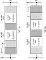
- the floating base could also be the n-doped base of the pnp, instead of the p-doped base of the npn, as shown in Figure 3a .
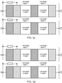
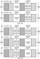
- the low doped regions might be n-doped or p-doped, as shown in Figures 3c and 3 d.
- the low doped regions might even be a sandwich of n- and p-doped layers, as shown in Figures 3e and 3 f.
- a semiconductor device comprises a trigger connection 230.
- Such the trigger connection 230 defines the breakdown voltage (BV).
- the semiconductor device comprises:
- the trigger connection will inject current, thus forward biasing the right np junction.
- the injected electrons will be collected at the left n-well and cause a voltage drop in that well that will eventually forward bias the left pn junction and start the conducting mode of the SCR.
- FIG. 5 An embodiment of the invention is shown in Figure 5 .
- a higher doped anti-punch layer may surround n-regions on all sides. This can be realized with a buried layer 250.
- the buried layer 250 can be of p-type.
- the semiconductor device comprises two buried layers: a first buried layer 250 and a second buried layer 252.
- the first buried layer 250 can be of p-type
- the second buried layer 252 can be of n-type.
- These two buried layers additionally isolate the SCR from the carrier substrate.
- Embodiments of the invention are shown in Figures 7a and 7b .
- the SCR is isolated from the carrier substrate with a buried oxide 260.
- the buried oxide 260 can be based on silicon on insulator (SOI) technology.
- SOI silicon on insulator
- the embodiment shown in Figure 7b comprises a buried oxide 260 that is touching the first n region 262.
- Embodiment of the invention are shown in Figures 8a and 8b .
- a sidewall isolation is provided. This can be implemented by a first sidewall isolation 290 and a second sidewall isolation 292.
- the sidewall isolation 290, 292 can be implemented as trenches or diffusions.
- FIG 8a shows a semiconductor device comprising a first buried layer 294 and a second buried layer 296, the second buried layer 296 positioned below the first buried layer 294.
- FIG. 8b shows a semiconductor device comprising a buried oxide 298.
- the previous embodiments relate to a one-direction-only SCR.
- the invention is also related to a two-direction/bidirectional SCR.
- the two-direction SCR behaves similar for both polarities.
- One possibility to realize a two-direction SCR is to copy the whole structure of a one-direction-only SCR and pasting it with a lateral shift.
- the bidirectional concept can easily be extended to a multi finger array structure with many SCRs in parallel.
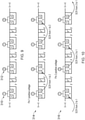
- An embodiment of the invention is shown in Figure 9 .
- the current goes always to right, regardless if pin 1 (reference 310 in Figure 9 ) is having a positive voltage (reference 314 in Figure 10 ) or pin 2 (reference 312 in Figure 9 ) is having a positive voltage (reference 316 in Figure 10 ).
- the current paths for positive and for negative voltage at pin 1 do not overlap, since they are placed at separate positions in the semiconductor device. Furthermore, the current direction is identical for both polarities.
- FIG 11 An embodiment of the invention is shown in Figure 11 .
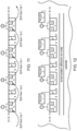
- This is a multi finger structure arrangement, with a buried isolation and a trigger injection, as shown in Figure 12 .
- local a trigger stripe 330 can be used instead of a trigger connection (as shown in Figure 4 , with the reference number 230).
- This semiconductor device with the local trigger stripe can be combined with the isolation methods, as described in the embodiments above, and can also be arranged in a multi-finger arrangement.
- the breakdown voltage between the trigger stripe and the n-well can be tailored to an actual voltage target.
- the trigger stripes 330 in a multi-finger arrangement are shown in an embodiment if the invention in Figure 14 .
- a trigger current is provided by an open base structure. This a npn transistor with a floating base. The breakdown voltage is well below 6 Volts, nonetheless, the trigger has a low leakage current. Therefore, the SCR will have a trigger voltage below 6 Volt.
- the trigger device In order to keep the parasitic capacitance small, the trigger device has to be small. But it has to be big enough to be able to deliver the necessary trigger current.
- FIG. 15 A cross section of such a semiconductor device is shown in Figure 15 . As it is shown in Figure 15 , below 6V there is still not leakage. The trigger voltage is much bellow 6V, i.e. 2-3V.
- the breakdown voltage can be fine-tuned with a dedicated p-well diffusion.
- the layout will be optimized for the best combination of a low voltage at a trigger current and a low parasitic capacitance.
- transistors can be built so that the gain is large for low current levels.
- the snap back voltage is reached at low current levels. The snap back can be reduced drastically.
- the open base transistor according to an embodiment of the invention is having the advantage that it can reach a breakdown voltage down to 2-4 V and still have very low leakage currents.
- FIGS 17a, 17b and 17c Three exemplary embodiments of the invention for the open base transistors are shown in Figures 17a, 17b and 17c .
- a vertical transistor is shown in Figure 17a .
- the gain is high at low currents because the base is nearly the same size as the collector.
- the overlap of p and n is minimized, so that the electrons that are injected from the emitter cannot go astray.
- FIG. 17b A transistor based in a process using a silicon on an insulator is shown in Figure 17b .
- the buried oxide acts as a barrier for the emitted electrons, so that nearly all injected electrons end in the collector.
- a third embodiment of an open base transistor is shown in Figure 17c .
- the buried player reflects the injected electrons. This improves the current gain for low current levels.
- This open base transistor has a breakdown voltage of about 3 V and a very low leakage current. It is therefore best used as a trigger current source for a SCR.
- the SCR than shows a very low trigger voltage and low leakage current.
Landscapes
- Semiconductor Integrated Circuits (AREA)
- Bipolar Integrated Circuits (AREA)
- Bipolar Transistors (AREA)
Priority Applications (3)
| Application Number | Priority Date | Filing Date | Title |
|---|---|---|---|
| EP20189593.5A EP3951884A1 (de) | 2020-08-05 | 2020-08-05 | Halbleiterbauelement und verfahren zur herstellung eines halbleiterbauelements |
| US17/394,080 US11984515B2 (en) | 2020-08-05 | 2021-08-04 | Semiconductor device and a method of manufacture of a semiconductor device |
| CN202110894943.3A CN114068520A (zh) | 2020-08-05 | 2021-08-05 | 半导体装置和半导体装置的制造方法 |
Applications Claiming Priority (1)
| Application Number | Priority Date | Filing Date | Title |
|---|---|---|---|
| EP20189593.5A EP3951884A1 (de) | 2020-08-05 | 2020-08-05 | Halbleiterbauelement und verfahren zur herstellung eines halbleiterbauelements |
Publications (1)
| Publication Number | Publication Date |
|---|---|
| EP3951884A1 true EP3951884A1 (de) | 2022-02-09 |
Family
ID=71950500
Family Applications (1)
| Application Number | Title | Priority Date | Filing Date |
|---|---|---|---|
| EP20189593.5A Pending EP3951884A1 (de) | 2020-08-05 | 2020-08-05 | Halbleiterbauelement und verfahren zur herstellung eines halbleiterbauelements |
Country Status (3)
| Country | Link |
|---|---|
| US (1) | US11984515B2 (de) |
| EP (1) | EP3951884A1 (de) |
| CN (1) | CN114068520A (de) |
Families Citing this family (1)
| Publication number | Priority date | Publication date | Assignee | Title |
|---|---|---|---|---|
| CN115911183B (zh) * | 2022-12-16 | 2026-04-17 | 复旦大学 | 一种雪崩光电二极管器件及其制备方法 |
Citations (4)
| Publication number | Priority date | Publication date | Assignee | Title |
|---|---|---|---|---|
| US3858235A (en) * | 1971-07-05 | 1974-12-31 | Siemens Ag | Planar four-layer-diode having a lateral arrangement of one of two partial transistors |
| US6236087B1 (en) * | 1998-11-02 | 2001-05-22 | Analog Devices, Inc. | SCR cell for electrical overstress protection of electronic circuits |
| US20110204415A1 (en) * | 2010-02-22 | 2011-08-25 | Sofics Bvba | High holding voltage device |
| EP2947691A1 (de) * | 2014-05-19 | 2015-11-25 | Nxp B.V. | Halbleiterbauelement |
Family Cites Families (9)
| Publication number | Priority date | Publication date | Assignee | Title |
|---|---|---|---|---|
| US20100193904A1 (en) * | 2009-01-30 | 2010-08-05 | Watt Jeffrey T | Integrated circuit inductor with doped substrate |
| US8193560B2 (en) * | 2009-06-18 | 2012-06-05 | Freescale Semiconductor, Inc. | Voltage limiting devices |
| US8441031B2 (en) * | 2011-01-28 | 2013-05-14 | Nxp B.V. | ESD protection device |
| TWI538154B (zh) * | 2013-10-23 | 2016-06-11 | 美商微晶片科技公司 | 晶片與靜電放電保護元件及其製造方法 |
| EP3407385B1 (de) * | 2017-05-23 | 2024-03-13 | NXP USA, Inc. | Zum schutz vor elektrostatischer entladung (esd) geeignetes halbleiterbauelement |
| US10700187B2 (en) * | 2018-05-30 | 2020-06-30 | Silanna Asia Pte Ltd | Tiled lateral thyristor |
| US11056481B2 (en) * | 2018-08-13 | 2021-07-06 | Amazing Microelectronic Corp. | Floating base silicon controlled rectifier |
| KR20200104448A (ko) * | 2019-02-26 | 2020-09-04 | 에스케이하이닉스 주식회사 | 보호 회로를 포함하는 반도체 집적 회로 및 반도체 집적 회로 구조체 |
| EP3761362A1 (de) * | 2019-07-03 | 2021-01-06 | Infineon Technologies AG | Siliciumgesteuerter gleichrichter |
-
2020
- 2020-08-05 EP EP20189593.5A patent/EP3951884A1/de active Pending
-
2021
- 2021-08-04 US US17/394,080 patent/US11984515B2/en active Active
- 2021-08-05 CN CN202110894943.3A patent/CN114068520A/zh active Pending
Patent Citations (4)
| Publication number | Priority date | Publication date | Assignee | Title |
|---|---|---|---|---|
| US3858235A (en) * | 1971-07-05 | 1974-12-31 | Siemens Ag | Planar four-layer-diode having a lateral arrangement of one of two partial transistors |
| US6236087B1 (en) * | 1998-11-02 | 2001-05-22 | Analog Devices, Inc. | SCR cell for electrical overstress protection of electronic circuits |
| US20110204415A1 (en) * | 2010-02-22 | 2011-08-25 | Sofics Bvba | High holding voltage device |
| EP2947691A1 (de) * | 2014-05-19 | 2015-11-25 | Nxp B.V. | Halbleiterbauelement |
Non-Patent Citations (1)
| Title |
|---|
| ANONYMOUS: "Depletion region - Wikipedia, the free encyclopedia", 14 May 2014 (2014-05-14), XP055219647, Retrieved from the Internet <URL:https://en.wikipedia.org/w/index.php?title=Depletion_region&oldid=608476441> [retrieved on 20151009] * |
Also Published As
| Publication number | Publication date |
|---|---|
| CN114068520A (zh) | 2022-02-18 |
| US11984515B2 (en) | 2024-05-14 |
| US20220045222A1 (en) | 2022-02-10 |
Similar Documents
| Publication | Publication Date | Title |
|---|---|---|
| US10211196B2 (en) | Electrostatic discharge protection device and electronic device having the same | |
| JP4006398B2 (ja) | 静電放電保護デバイスを有する集積回路 | |
| US7582936B2 (en) | Electro-static discharge protection circuit and method for fabricating the same | |
| US9576945B2 (en) | Methods and apparatus for increased holding voltage in silicon controlled rectifiers for ESD protection | |
| US9685443B2 (en) | Compact guard ring structure for CMOS integrated circuits | |
| US6594132B1 (en) | Stacked silicon controlled rectifiers for ESD protection | |
| US8455949B2 (en) | ESD protection element and ESD protection device for use in an electrical circuit | |
| US8692289B2 (en) | Fast turn on silicon controlled rectifiers for ESD protection | |
| US9443840B2 (en) | Methods and apparatus for ESD structures | |
| US8623731B2 (en) | Methods of forming electrostatic discharge devices | |
| US10373944B2 (en) | ESD protection circuit with integral deep trench trigger diodes | |
| US20090267154A1 (en) | Mos comprising substrate potential elevating circuitry for esd protection | |
| US20080023767A1 (en) | High voltage electrostatic discharge protection devices and electrostatic discharge protection circuits | |
| US20130320485A1 (en) | Semiconductor device | |
| US11508723B2 (en) | Power semiconductor device with a temperature sensor | |
| US7235846B2 (en) | ESD protection structure with SiGe BJT devices | |
| US11984515B2 (en) | Semiconductor device and a method of manufacture of a semiconductor device | |
| US6469365B1 (en) | Semiconductor component with a structure for avoiding parallel-path currents and method for fabricating a semiconductor component | |
| CN119789534A (zh) | 一种双向栅控可控硅结构 | |
| CN112447703A (zh) | 静电放电防护元件 | |
| US9881913B2 (en) | Bipolar SCR | |
| EP4376079A1 (de) | Halbleiteranordnung | |
| US20260114250A1 (en) | Semiconductor device with multi-body bias using deep trench isolation | |
| US11967639B2 (en) | SCR structure for ESD protection in SOI technologies | |
| KR102361561B1 (ko) | 향상된 스냅백 특성을 갖는 정전기 방전 보호소자 |
Legal Events
| Date | Code | Title | Description |
|---|---|---|---|
| PUAI | Public reference made under article 153(3) epc to a published international application that has entered the european phase |
Free format text: ORIGINAL CODE: 0009012 |
|
| STAA | Information on the status of an ep patent application or granted ep patent |
Free format text: STATUS: THE APPLICATION HAS BEEN PUBLISHED |
|
| AK | Designated contracting states |
Kind code of ref document: A1 Designated state(s): AL AT BE BG CH CY CZ DE DK EE ES FI FR GB GR HR HU IE IS IT LI LT LU LV MC MK MT NL NO PL PT RO RS SE SI SK SM TR |
|
| STAA | Information on the status of an ep patent application or granted ep patent |
Free format text: STATUS: REQUEST FOR EXAMINATION WAS MADE |
|
| 17P | Request for examination filed |
Effective date: 20220808 |
|
| RBV | Designated contracting states (corrected) |
Designated state(s): AL AT BE BG CH CY CZ DE DK EE ES FI FR GB GR HR HU IE IS IT LI LT LU LV MC MK MT NL NO PL PT RO RS SE SI SK SM TR |