EP3957776B1 - Procédé de dépôt d'une couche épitaxiée sur une tranche de substrat - Google Patents
Procédé de dépôt d'une couche épitaxiée sur une tranche de substrat Download PDFInfo
- Publication number
- EP3957776B1 EP3957776B1 EP20191322.5A EP20191322A EP3957776B1 EP 3957776 B1 EP3957776 B1 EP 3957776B1 EP 20191322 A EP20191322 A EP 20191322A EP 3957776 B1 EP3957776 B1 EP 3957776B1
- Authority
- EP
- European Patent Office
- Prior art keywords
- substrate wafer
- edge
- epitaxial layer
- thickness
- Prior art date
- Legal status (The legal status is an assumption and is not a legal conclusion. Google has not performed a legal analysis and makes no representation as to the accuracy of the status listed.)
- Active
Links
Images



Classifications
-
- C—CHEMISTRY; METALLURGY
- C30—CRYSTAL GROWTH
- C30B—SINGLE-CRYSTAL GROWTH; UNIDIRECTIONAL SOLIDIFICATION OF EUTECTIC MATERIAL OR UNIDIRECTIONAL DEMIXING OF EUTECTOID MATERIAL; REFINING BY ZONE-MELTING OF MATERIAL; PRODUCTION OF A HOMOGENEOUS POLYCRYSTALLINE MATERIAL WITH DEFINED STRUCTURE; SINGLE CRYSTALS OR HOMOGENEOUS POLYCRYSTALLINE MATERIAL WITH DEFINED STRUCTURE; AFTER-TREATMENT OF SINGLE CRYSTALS OR A HOMOGENEOUS POLYCRYSTALLINE MATERIAL WITH DEFINED STRUCTURE; APPARATUS THEREFOR
- C30B25/00—Single-crystal growth by chemical reaction of reactive gases, e.g. chemical vapour-deposition growth
- C30B25/02—Epitaxial-layer growth
- C30B25/16—Controlling or regulating
-
- C—CHEMISTRY; METALLURGY
- C23—COATING METALLIC MATERIAL; COATING MATERIAL WITH METALLIC MATERIAL; CHEMICAL SURFACE TREATMENT; DIFFUSION TREATMENT OF METALLIC MATERIAL; COATING BY VACUUM EVAPORATION, BY SPUTTERING, BY ION IMPLANTATION OR BY CHEMICAL VAPOUR DEPOSITION, IN GENERAL; INHIBITING CORROSION OF METALLIC MATERIAL OR INCRUSTATION IN GENERAL
- C23C—COATING METALLIC MATERIAL; COATING MATERIAL WITH METALLIC MATERIAL; SURFACE TREATMENT OF METALLIC MATERIAL BY DIFFUSION INTO THE SURFACE, BY CHEMICAL CONVERSION OR SUBSTITUTION; COATING BY VACUUM EVAPORATION, BY SPUTTERING, BY ION IMPLANTATION OR BY CHEMICAL VAPOUR DEPOSITION, IN GENERAL
- C23C16/00—Chemical coating by decomposition of gaseous compounds, without leaving reaction products of surface material in the coating, i.e. chemical vapour deposition [CVD] processes
- C23C16/44—Chemical coating by decomposition of gaseous compounds, without leaving reaction products of surface material in the coating, i.e. chemical vapour deposition [CVD] processes characterised by the method of coating
- C23C16/458—Chemical coating by decomposition of gaseous compounds, without leaving reaction products of surface material in the coating, i.e. chemical vapour deposition [CVD] processes characterised by the method of coating characterised by the method used for supporting substrates in the reaction chamber
- C23C16/4582—Rigid and flat substrates, e.g. plates or discs
- C23C16/4583—Rigid and flat substrates, e.g. plates or discs the substrate being supported substantially horizontally
- C23C16/4585—Devices at or outside the perimeter of the substrate support, e.g. clamping rings, shrouds
-
- C—CHEMISTRY; METALLURGY
- C23—COATING METALLIC MATERIAL; COATING MATERIAL WITH METALLIC MATERIAL; CHEMICAL SURFACE TREATMENT; DIFFUSION TREATMENT OF METALLIC MATERIAL; COATING BY VACUUM EVAPORATION, BY SPUTTERING, BY ION IMPLANTATION OR BY CHEMICAL VAPOUR DEPOSITION, IN GENERAL; INHIBITING CORROSION OF METALLIC MATERIAL OR INCRUSTATION IN GENERAL
- C23C—COATING METALLIC MATERIAL; COATING MATERIAL WITH METALLIC MATERIAL; SURFACE TREATMENT OF METALLIC MATERIAL BY DIFFUSION INTO THE SURFACE, BY CHEMICAL CONVERSION OR SUBSTITUTION; COATING BY VACUUM EVAPORATION, BY SPUTTERING, BY ION IMPLANTATION OR BY CHEMICAL VAPOUR DEPOSITION, IN GENERAL
- C23C16/00—Chemical coating by decomposition of gaseous compounds, without leaving reaction products of surface material in the coating, i.e. chemical vapour deposition [CVD] processes
- C23C16/44—Chemical coating by decomposition of gaseous compounds, without leaving reaction products of surface material in the coating, i.e. chemical vapour deposition [CVD] processes characterised by the method of coating
- C23C16/52—Controlling or regulating the coating process
-
- C—CHEMISTRY; METALLURGY
- C30—CRYSTAL GROWTH
- C30B—SINGLE-CRYSTAL GROWTH; UNIDIRECTIONAL SOLIDIFICATION OF EUTECTIC MATERIAL OR UNIDIRECTIONAL DEMIXING OF EUTECTOID MATERIAL; REFINING BY ZONE-MELTING OF MATERIAL; PRODUCTION OF A HOMOGENEOUS POLYCRYSTALLINE MATERIAL WITH DEFINED STRUCTURE; SINGLE CRYSTALS OR HOMOGENEOUS POLYCRYSTALLINE MATERIAL WITH DEFINED STRUCTURE; AFTER-TREATMENT OF SINGLE CRYSTALS OR A HOMOGENEOUS POLYCRYSTALLINE MATERIAL WITH DEFINED STRUCTURE; APPARATUS THEREFOR
- C30B25/00—Single-crystal growth by chemical reaction of reactive gases, e.g. chemical vapour-deposition growth
- C30B25/02—Epitaxial-layer growth
- C30B25/12—Substrate holders or susceptors
-
- C—CHEMISTRY; METALLURGY
- C30—CRYSTAL GROWTH
- C30B—SINGLE-CRYSTAL GROWTH; UNIDIRECTIONAL SOLIDIFICATION OF EUTECTIC MATERIAL OR UNIDIRECTIONAL DEMIXING OF EUTECTOID MATERIAL; REFINING BY ZONE-MELTING OF MATERIAL; PRODUCTION OF A HOMOGENEOUS POLYCRYSTALLINE MATERIAL WITH DEFINED STRUCTURE; SINGLE CRYSTALS OR HOMOGENEOUS POLYCRYSTALLINE MATERIAL WITH DEFINED STRUCTURE; AFTER-TREATMENT OF SINGLE CRYSTALS OR A HOMOGENEOUS POLYCRYSTALLINE MATERIAL WITH DEFINED STRUCTURE; APPARATUS THEREFOR
- C30B25/00—Single-crystal growth by chemical reaction of reactive gases, e.g. chemical vapour-deposition growth
- C30B25/02—Epitaxial-layer growth
- C30B25/18—Epitaxial-layer growth characterised by the substrate
-
- C—CHEMISTRY; METALLURGY
- C30—CRYSTAL GROWTH
- C30B—SINGLE-CRYSTAL GROWTH; UNIDIRECTIONAL SOLIDIFICATION OF EUTECTIC MATERIAL OR UNIDIRECTIONAL DEMIXING OF EUTECTOID MATERIAL; REFINING BY ZONE-MELTING OF MATERIAL; PRODUCTION OF A HOMOGENEOUS POLYCRYSTALLINE MATERIAL WITH DEFINED STRUCTURE; SINGLE CRYSTALS OR HOMOGENEOUS POLYCRYSTALLINE MATERIAL WITH DEFINED STRUCTURE; AFTER-TREATMENT OF SINGLE CRYSTALS OR A HOMOGENEOUS POLYCRYSTALLINE MATERIAL WITH DEFINED STRUCTURE; APPARATUS THEREFOR
- C30B29/00—Single crystals or homogeneous polycrystalline material with defined structure characterised by the material or by their shape
- C30B29/02—Elements
- C30B29/06—Silicon
-
- H—ELECTRICITY
- H10—SEMICONDUCTOR DEVICES; ELECTRIC SOLID-STATE DEVICES NOT OTHERWISE PROVIDED FOR
- H10P—GENERIC PROCESSES OR APPARATUS FOR THE MANUFACTURE OR TREATMENT OF DEVICES COVERED BY CLASS H10
- H10P74/00—Testing or measuring during manufacture or treatment of wafers, substrates or devices
- H10P74/20—Testing or measuring during manufacture or treatment of wafers, substrates or devices characterised by the properties tested or measured, e.g. structural or electrical properties
- H10P74/203—Structural properties, e.g. testing or measuring thicknesses, line widths, warpage, bond strengths or physical defects
Definitions
- the invention relates to a method for depositing an epitaxial layer on a substrate wafer.
- epitaxially coated semiconductor wafers in particular substrate wafers made of single-crystal silicon, which are epitaxially coated with a layer of silicon, are required.
- a frequently used method for depositing the layer is vapor deposition.
- the material for the layer is provided by process gas, which is passed over the side of the substrate wafer to be coated at temperatures at which a precursor compound contained in the process gas, which contains the material, chemically cleaves.
- the substrate wafer lies in the pocket of a susceptor, surrounded by an annular boundary of the susceptor.
- the process is usually carried out in a device designed as a single-wafer reactor. Such a single-wafer reactor is used, for example, in EP 0 870 852 A1 described.
- the substrate wafer is positioned centrally to the boundary in the pocket.
- WO 14 103 657 A1 and JP2015 201 599 A disclose methods which calculate an eccentricity based on the distribution of thickness parameters in the edge region of the semiconductor wafer with epitaxially deposited layer in order to correct the position of a subsequent substrate wafer on the susceptor depending on this eccentricity.
- US2009 252 942 A1 and JP2002 043 230 A propose to measure the flatness of the substrate wafer before depositing the epitaxial layer and to change certain process parameters during deposition so that edge drop is reduced as the substrate wafer is coated.
- the object of the invention is to offer a solution to the problem which makes it possible to adjust the thickness of the epitaxial layer in the edge region differently at different positions of the circumference of the substrate wafer.
- the invention is based on the finding that the centered placement of the substrate wafer in the pocket is accompanied by the expectation that the substrate wafer will have a uniform edge geometry. In practice, however, this is rarely the case because processing steps such as grinding and polishing are not capable of creating a substrate wafer with a completely uniform edge thickness.
- the method according to the invention is capable of standardizing the edge geometry of an epitaxially coated semiconductor wafer compared to an uncoated substrate wafer, in particular when the substrate wafer has a comparatively thin edge thickness in one edge section and a comparatively thick edge thickness in the opposite edge section. Notwithstanding this, homogenization of the edge thickness can also be achieved if, for example, only one edge section with a comparatively thin edge thickness is present.
- the edge geometry of the substrate wafer is measured so that it is available in the form of a thickness parameter.
- a thickness parameter Preferably, an outermost edge piece with a radial length of 1 mm or 2 mm is excluded from the measurement as an edge exclusion.
- any measured value that allows a statement to be made about the relative thickness at two different sections in the edge region of the substrate wafer can be used as a thickness parameter.
- the ZDD (Z double derivative) of the front side which describes the curvature of the edge drop and is defined in the SEMI standard M68-0720
- the ESFQR which quantifies the flatness of sectors (sites) in the edge region and is defined in the SEMI standard M67-0720
- the following description uses ESFQR as a representative thickness parameter.
- the method according to the invention provides for measuring the edge geometry of a substrate wafer before coating it with an epitaxial layer. This results in, for example, a map that assigns an ESFQR value to each sector and thus displays a thickness profile of the substrate wafer along its circumference.
- Substrate wafers with a wedge-shaped cross-section or those that are Thinner at one edge section than at others are particularly suitable.
- An edge section refers to an edge region that extends over a distance of up to 50% of the circumference, preferably 7% to 42% of the circumference in the circumferential direction.
- a wedge-shaped substrate wafer has a thicker edge section and a thinner edge section that are opposite each other, i.e., are spaced as far apart as possible.
- a correlation function assigns a thickness value to a displacement vector.
- the displacement vector indicates the direction and amount by which the substrate wafer, with the thicker edge section, must be placed into the pocket of the susceptor offset from its centered position so that more material is deposited on the opposite, thinner edge section during deposition of the epitaxial layer than on the thicker edge section. Accordingly, the thickness value after deposition in the thinner edge section of the substrate wafer is greater by the assigned thickness value than it would be after the deposition of an epitaxial layer during which the substrate wafer lies centered in the pocket of the susceptor.
- the displacement vector therefore represents an eccentricity of the position of the center point of the substrate wafer lying on the susceptor compared to the position the center point would have if the substrate wafer were centered in the pocket of the susceptor.
- the correlation function is determined by experiments before coating the substrate wafer by determining which eccentricity results in which change in the thickness parameter.
- the placement of the substrate wafer into the pocket of the susceptor is preferably carried out by a robot, which carries out this task according to the correlation function.
- the robot can be configured as a self-learning system, which uses the measured geometry data of the substrate wafers and the resulting epitaxially coated semiconductor wafers to determine and implement the necessary eccentricity for the coating of subsequent substrate wafers.
- the substrate wafer and the epitaxial layer deposited thereon preferably consist essentially of semiconductor material, for example, monocrystalline silicon.
- the substrate wafer preferably has a diameter of at least 200 mm, particularly preferably at least 300 mm.
- the epitaxial layer preferably has a thickness of 1 ⁇ m to 20 ⁇ m.
- Fig.1 shows a sectional view (vertical section) of a substrate wafer 1 deposited in the pocket 4 of a susceptor 3, which has a comparatively thick edge section 5 and an opposite, comparatively thin edge section 6.
- the substrate wafer 1 is not centered in the pocket 4, but rather eccentrically, such that the thicker edge section 5 is a smaller distance from a boundary 7 of the pocket than the thinner edge section 6.
- This configuration has the consequence that where the distance is smaller, the rate of material growth during the deposition of the epitaxial layer is lower than where the distance is larger.
- the lower part of Fig.1 shows the situation after the deposition of the epitaxial layer 2.
- the substrate wafer 1 has become a substrate wafer with a deposited epitaxial layer, wherein the epitaxial layer 2 is thinner in the region of the edge section with a smaller distance to the boundary 4 than in the region of the edge section with a greater distance to the boundary 4.
- the thickness of the substrate wafer with deposited epitaxial layer 2 is considered and compared with the thickness of the substrate wafer 1, it can be seen that the thickness of the epitaxially coated substrate wafer in its edge region is more uniform than the thickness of the substrate wafer 1.
- the differences in thickness in the edge region are in the case of Substrate wafer 1 is more pronounced than in the case of the epitaxially coated substrate wafer.
- Fig. 2 shows a plan view of a substrate wafer placed in the pocket of the susceptor according to the invention.
- the substrate wafer 1 is not centered in the pocket of the susceptor.
- the center of the substrate wafer is shifted from the center of the pocket according to the eccentricity E, specifically such that the thicker edge section 6 is a smaller distance from the outer boundary 7 of the pocket than the thinner edge section 6.
- the direction and magnitude of the eccentricity E depend on a measurement of the edge geometry of the substrate wafer, for example, by measuring the flatness in 5° wide edge segments in the form of the ESFQR value.
- the result of the measurement is qualitatively indicated by the map 8 and shows the thicker edge section 5 highlighted with "+" symbols and the thinner edge section 6 highlighted with "-" symbols.
- the selected eccentricity E is based on a correlation function determined through preliminary tests for the deposition device used. This investigates the change in the thickness parameter that can be expected when the substrate wafer is deposited in the pocket of the susceptor with a specific eccentricity E.
- the correlation function according to Fig. 3 which difference ⁇ ESFQR of the ESFQR value in the thinner edge section is obtained after deposition if the substrate wafer is not placed centrally but with the corresponding eccentricity E in the pocket of the susceptor before deposition.
- the ESFQR value in the sectors of the thinner edge section will be approximately 2 nm higher, provided that the substrate wafer was not placed centrally but with an eccentricity of 100 ⁇ m in the pocket of the susceptor before deposition.
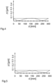
- Fig. 4, Fig. 5 and Fig. 6 show the course of the deviation of a thickness from a target thickness of a substrate wafer made of single-crystalline silicon ( Fig. 4 ) and after ( Fig. 5 ) the deposition of an epitaxial layer and the deviation of the thickness of the epitaxial layer ( Fig. 6 ) of a target thickness.
- the substrate disc had significantly different edge thicknesses, with a thinner Edge section in the range of 0 mm and a thicker edge section in the range of 300 mm. After deposition of the epitaxial layer according to the present invention, the difference in edge thickness in these edge sections was almost equalized ( Fig. 5 ).
- the epitaxial layer is thicker at the edge position corresponding to the thinner edge section of the substrate wafer and thinner at the edge position corresponding to the thicker edge section of the substrate wafer.
- the eccentric position of the substrate wafer resulted in different amounts of material being deposited at the edge sections under consideration.
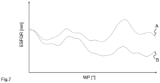
- Fig. 7 shows, in the form of smoothed curves, the edge geometry of a substrate wafer before (curve A) and after (curve B) the deposition of an epitaxial layer, in the form of the ESFQR value as a function of the edge position WP.
- the curves are based on 72 measurement points, each of which describes the ESFQR value of a sector with a width of 5° and a radial length of 35 mm, taking into account an edge exclusion of 1 mm.
Landscapes
- Chemical & Material Sciences (AREA)
- Engineering & Computer Science (AREA)
- Materials Engineering (AREA)
- Metallurgy (AREA)
- Organic Chemistry (AREA)
- Chemical Kinetics & Catalysis (AREA)
- General Chemical & Material Sciences (AREA)
- Crystallography & Structural Chemistry (AREA)
- Mechanical Engineering (AREA)
- Crystals, And After-Treatments Of Crystals (AREA)
- Container, Conveyance, Adherence, Positioning, Of Wafer (AREA)
- Chemical Vapour Deposition (AREA)
Claims (4)
- Procédé de dépôt d'une couche épitaxiale sur une tranche de substrat à partir d'une phase gazeuse, comprenantla mesure d'une géométrie du bord de la tranche de substrat, qui attribue une valeur d'épaisseur à un bord de la tranche de substrat en fonction de positions de bord, la tranche de substrat présentant une partie de bord plus épaisse et une partie de bord plus mince qui se font face ;le placement de la tranche de substrat dans une poche d'un suscepteur d'un dispositif destiné au dépôt de la couche épitaxiale, la poche étant entourée d'une délimitation ayant un périmètre circulaire ;le chauffage de la tranche de substrat ; etle passage de gaz de processus sur la tranche de substrat ;caractérisé parle placement de la tranche de substrat dans la poche de façon telle qu'un espacement que présente la tranche de substrat par rapport à la délimitation de la poche est plus court aux positions de bord de la partie de bord plus épaisse à plus grande valeur d'épaisseur qu'aux positions de bord de la partie de bord plus mince à plus faible valeur d'épaisseur, la valeur d'épaisseur étant soit la ZDD, définie selon la norme SEMI M68-0720, de la face avant, soit le ESFOR défini selon la norme SEMI M67-0720.
- Procédé selon la revendication 1, caractérisé par le placement de la tranche de substrat au moyen d'un robot.
- Procédé selon la revendication 1 ou 2, caractérisé par la surveillance de la position de la tranche de substrat dans la poche au moyen d'un système de caméra.
- Procédé selon l'une quelconque des revendications 1 à 3, caractérisé par le dépôt d'une couche épitaxiale de silicium sur une tranche de substrat en silicium monocristallin.
Priority Applications (8)
| Application Number | Priority Date | Filing Date | Title |
|---|---|---|---|
| EP20191322.5A EP3957776B1 (fr) | 2020-08-17 | 2020-08-17 | Procédé de dépôt d'une couche épitaxiée sur une tranche de substrat |
| KR1020237007497A KR102753834B1 (ko) | 2020-08-17 | 2021-07-21 | 기판 웨이퍼 상에 에피택셜층을 퇴적하기 위한 방법 |
| CN202180055480.XA CN116057202B (zh) | 2020-08-17 | 2021-07-21 | 用于在衬底晶圆上沉积外延层的方法 |
| US18/040,991 US12331424B2 (en) | 2020-08-17 | 2021-07-21 | Method for depositing an epitaxial layer on a substrate wafer |
| PCT/EP2021/070393 WO2022037889A1 (fr) | 2020-08-17 | 2021-07-21 | Procédé de dépôt d'une couche épitaxiale sur une plaquette de substrat |
| JP2023511961A JP7537008B2 (ja) | 2020-08-17 | 2021-07-21 | 基板ウェハ上にエピタキシャル層を堆積させるための方法 |
| TW110128428A TWI777712B (zh) | 2020-08-17 | 2021-08-02 | 用於在基板晶圓上沉積磊晶層的方法 |
| IL300448A IL300448B2 (en) | 2020-08-17 | 2023-02-06 | Method for depositing an epitaxial layer on a substrate wafer |
Applications Claiming Priority (1)
| Application Number | Priority Date | Filing Date | Title |
|---|---|---|---|
| EP20191322.5A EP3957776B1 (fr) | 2020-08-17 | 2020-08-17 | Procédé de dépôt d'une couche épitaxiée sur une tranche de substrat |
Publications (2)
| Publication Number | Publication Date |
|---|---|
| EP3957776A1 EP3957776A1 (fr) | 2022-02-23 |
| EP3957776B1 true EP3957776B1 (fr) | 2025-06-18 |
Family
ID=72145221
Family Applications (1)
| Application Number | Title | Priority Date | Filing Date |
|---|---|---|---|
| EP20191322.5A Active EP3957776B1 (fr) | 2020-08-17 | 2020-08-17 | Procédé de dépôt d'une couche épitaxiée sur une tranche de substrat |
Country Status (8)
| Country | Link |
|---|---|
| US (1) | US12331424B2 (fr) |
| EP (1) | EP3957776B1 (fr) |
| JP (1) | JP7537008B2 (fr) |
| KR (1) | KR102753834B1 (fr) |
| CN (1) | CN116057202B (fr) |
| IL (1) | IL300448B2 (fr) |
| TW (1) | TWI777712B (fr) |
| WO (1) | WO2022037889A1 (fr) |
Families Citing this family (2)
| Publication number | Priority date | Publication date | Assignee | Title |
|---|---|---|---|---|
| EP3978647A1 (fr) * | 2020-09-30 | 2022-04-06 | Siltronic AG | Procédé et dispositif de dépôt d'une couche épitactique sur un substrat en tranche en matière semi-conductrice |
| CN115852478B (zh) * | 2022-12-15 | 2025-04-04 | 西安奕斯伟材料科技股份有限公司 | 用于硅片的外延生长的基座及装置 |
Family Cites Families (25)
| Publication number | Priority date | Publication date | Assignee | Title |
|---|---|---|---|---|
| US6153260A (en) | 1997-04-11 | 2000-11-28 | Applied Materials, Inc. | Method for heating exhaust gas in a substrate reactor |
| JP2002009002A (ja) | 2000-06-26 | 2002-01-11 | Nec Kansai Ltd | 薄膜形成装置 |
| JP3897963B2 (ja) | 2000-07-25 | 2007-03-28 | 株式会社Sumco | 半導体ウェーハおよびその製造方法 |
| JP2002261023A (ja) | 2001-02-28 | 2002-09-13 | Shin Etsu Handotai Co Ltd | エピタキシャルウェーハの製造方法 |
| JP4899445B2 (ja) | 2005-11-22 | 2012-03-21 | 信越半導体株式会社 | エピタキシャルウェーハの製造方法及びエピタキシャルウェーハ |
| US8021484B2 (en) | 2006-03-30 | 2011-09-20 | Sumco Techxiv Corporation | Method of manufacturing epitaxial silicon wafer and apparatus therefor |
| JP4868522B2 (ja) | 2006-03-30 | 2012-02-01 | Sumco Techxiv株式会社 | エピタキシャルウェーハの製造方法及び製造装置 |
| KR101038876B1 (ko) | 2007-12-24 | 2011-06-02 | 삼성엘이디 주식회사 | 화학기상증착용 웨이퍼 및 이를 제조하는 방법 |
| US20090214843A1 (en) | 2008-02-26 | 2009-08-27 | Siltronic Corporation | Controlled edge resistivity in a silicon wafer |
| JP5098873B2 (ja) | 2008-07-30 | 2012-12-12 | 株式会社Sumco | 気相成長装置用のサセプタ及び気相成長装置 |
| US8575701B1 (en) * | 2009-01-13 | 2013-11-05 | Renesas Electronics Corporation | Semiconductor device where logic region and DRAM are formed on same substrate |
| DE102009010555A1 (de) | 2009-02-25 | 2010-09-02 | Siltronic Ag | Verfahren zum Erkennen einer Fehllage einer Halbleiterscheibe während einer thermischen Behandlung |
| DE102010029756B4 (de) * | 2010-06-07 | 2023-09-21 | Sicrystal Gmbh | Herstellungsverfahren für einen SiC-Volumeneinkristall mit großer Facette und einkristallines SiC-Substrat mit homogener Widerstandsverteilung |
| KR101496572B1 (ko) | 2012-10-16 | 2015-02-26 | 주식회사 엘지실트론 | 에피택셜 성장용 서셉터 및 에피택셜 성장방법 |
| JP5943201B2 (ja) | 2012-12-26 | 2016-06-29 | 信越半導体株式会社 | 偏芯評価方法及びエピタキシャルウェーハの製造方法 |
| DE102013203743A1 (de) | 2013-03-05 | 2014-09-11 | Heraeus Precious Metals Gmbh & Co. Kg | Verfahren zur Herstellung hochreinen Platinpulvers sowie Platinpulver erhältlich nach diesem Verfahren und Verwendung |
| US10099245B2 (en) * | 2013-03-14 | 2018-10-16 | Applied Materials, Inc. | Process kit for deposition and etching |
| JP6132163B2 (ja) | 2014-04-10 | 2017-05-24 | 信越半導体株式会社 | 偏芯評価方法及びエピタキシャルウェーハの製造方法 |
| DE102015220924B4 (de) | 2015-10-27 | 2018-09-27 | Siltronic Ag | Suszeptor zum Halten einer Halbleiterscheibe mit Orientierungskerbe, Verfahren zum Abscheiden einer Schicht auf einer Halbleiterscheibe und Halbleiterscheibe |
| KR101810643B1 (ko) * | 2016-02-02 | 2017-12-19 | 에스케이실트론 주식회사 | 에피텍셜 웨이퍼의 평탄도 제어 방법 |
| US10410832B2 (en) * | 2016-08-19 | 2019-09-10 | Lam Research Corporation | Control of on-wafer CD uniformity with movable edge ring and gas injection adjustment |
| JP6832770B2 (ja) | 2017-03-28 | 2021-02-24 | 昭和電工株式会社 | 熱化学蒸着装置の基板ホルダー |
| DE102017212799A1 (de) | 2017-07-26 | 2019-01-31 | Siltronic Ag | Epitaktisch beschichtete Halbleiterscheibe aus einkristallinem Silizium und Verfahren zu deren Herstellung |
| JP6968670B2 (ja) | 2017-11-17 | 2021-11-17 | 信越半導体株式会社 | サセプタ、エピタキシャルウェーハの製造方法 |
| JP6965861B2 (ja) | 2018-09-28 | 2021-11-10 | 信越半導体株式会社 | 気相成長装置 |
-
2020
- 2020-08-17 EP EP20191322.5A patent/EP3957776B1/fr active Active
-
2021
- 2021-07-21 JP JP2023511961A patent/JP7537008B2/ja active Active
- 2021-07-21 CN CN202180055480.XA patent/CN116057202B/zh active Active
- 2021-07-21 WO PCT/EP2021/070393 patent/WO2022037889A1/fr not_active Ceased
- 2021-07-21 KR KR1020237007497A patent/KR102753834B1/ko active Active
- 2021-07-21 US US18/040,991 patent/US12331424B2/en active Active
- 2021-08-02 TW TW110128428A patent/TWI777712B/zh active
-
2023
- 2023-02-06 IL IL300448A patent/IL300448B2/en unknown
Non-Patent Citations (2)
| Title |
|---|
| GHIM YOUNG-SIK ET AL: "Reflectometry-based wavelength scanning interferometry for thickness measurements of very thin wafers", OPTICS EXPRESS, vol. 18, no. 7, 29 March 2010 (2010-03-29), US, pages 6522, XP055938792, ISSN: 2161-2072, DOI: 10.1364/OE.18.006522 * |
| GRIESMANN ULF ET AL: "Manufacture and Metrology of 300 mm Silicon Wafers with Ultra-Low Thickness Variation", AIP CONFERENCE PROCEEDINGS, vol. 931, 1 January 2007 (2007-01-01), NEW YORK, US, pages 105 - 110, XP055938943, ISSN: 0094-243X, Retrieved from the Internet <URL:https://doi.org/10.1063/1.2799352?locatt=mode:legacy> DOI: 10.1063/1.2799352 * |
Also Published As
| Publication number | Publication date |
|---|---|
| KR20230045059A (ko) | 2023-04-04 |
| IL300448B1 (en) | 2026-04-01 |
| WO2022037889A1 (fr) | 2022-02-24 |
| IL300448B2 (en) | 2026-08-01 |
| US20230265581A1 (en) | 2023-08-24 |
| IL300448A (en) | 2023-04-01 |
| EP3957776A1 (fr) | 2022-02-23 |
| JP7537008B2 (ja) | 2024-08-20 |
| US12331424B2 (en) | 2025-06-17 |
| TW202221163A (zh) | 2022-06-01 |
| TWI777712B (zh) | 2022-09-11 |
| JP2023541796A (ja) | 2023-10-04 |
| KR102753834B1 (ko) | 2025-01-10 |
| CN116057202B (zh) | 2025-03-07 |
| CN116057202A (zh) | 2023-05-02 |
Similar Documents
| Publication | Publication Date | Title |
|---|---|---|
| DE112008003535T5 (de) | Suszeptor für das epitaxiale Wachstum | |
| DE60018125T2 (de) | Steurung der Ionendosis in einem Implantierungsgerät | |
| WO2022037889A1 (fr) | Procédé de dépôt d'une couche épitaxiale sur une plaquette de substrat | |
| DE102016210203B3 (de) | Suszeptor zum Halten einer Halbleiterscheibe, Verfahren zum Abscheiden einer epitaktischen Schicht auf einer Vorderseite einer Halbleiterscheibe und Halbleiterscheibe mit epitaktischer Schicht | |
| DE19957671A1 (de) | Werkzeug mit einer Molybdänsulfid enthaltenden Beschichtung und Verfahren zu dessen Herstellung | |
| EP3642866A2 (fr) | Procédé, système de commande et installation de traitement d'une plaquette de semi-conducteur et plaquette de semi-conducteur | |
| DE19703271A1 (de) | Materialprüfvorrichtung, Materialprüfgerät und Materialprüfverfahren | |
| WO2017102597A1 (fr) | Procédé pour effectuer le revêtement épitaxique de tranches de semi-conducteur et tranche de semi-conducteur | |
| DE102017212799A1 (de) | Epitaktisch beschichtete Halbleiterscheibe aus einkristallinem Silizium und Verfahren zu deren Herstellung | |
| EP3996130B1 (fr) | Procédé de dépôt d'une couche épitaxiée sur une tranche de substrat | |
| EP3475472B1 (fr) | Procédé et dispositif de fabrication de tranches semi-conductrices revêtues | |
| WO2006089435A1 (fr) | Procede de positionnement d'une plaquette | |
| DE3028536C2 (de) | Vorrichtung zur Halterung von kreisförmigen Substratscheiben und ihre Verwendung | |
| DE69315114T2 (de) | Epitaxie auf einem Substrat | |
| DE19516256C1 (de) | Vorrichtung zur in-situ Messung von mechanischen Spannungen in Schichten | |
| DE10000019A1 (de) | Sputtervorrichtung | |
| DE102020119873A1 (de) | Verfahren zum Erkennen fehlerhafter oder fehlerhaft in einem CVD-Reaktor eingesetzte Substrate | |
| EP4200459B1 (fr) | Procédé de dépôt physique en phase vapeur et dispositif associé | |
| EP3839109B1 (fr) | Procédé d'épitaxie en phase gazeuse | |
| DE102007061777B4 (de) | Verfahren zur Vakuumbeschichtung von zu beschichtenden Substraten und Vakkumbeschichtungsanlage | |
| EP3839105B1 (fr) | Procédé d'épitaxie en phase gazeuse | |
| EP4075489B1 (fr) | Procédé de fabrication de plaquettes semi-conductrices à couche épitaxiale déposée en phase gazeuse dans une chambre de dépôt | |
| EP2630653B1 (fr) | Dispositif de revêtement d'une tranche | |
| DE69110427T2 (de) | Verfahren zur Messung der Verschiebung eines Musters. | |
| DD282475A5 (de) | Einrichtung zur messung der abscheidungsrate und zur limitierung des beschichtungsprozesses in vakuumbeschichtungsanlagen |
Legal Events
| Date | Code | Title | Description |
|---|---|---|---|
| PUAI | Public reference made under article 153(3) epc to a published international application that has entered the european phase |
Free format text: ORIGINAL CODE: 0009012 |
|
| STAA | Information on the status of an ep patent application or granted ep patent |
Free format text: STATUS: THE APPLICATION HAS BEEN PUBLISHED |
|
| AK | Designated contracting states |
Kind code of ref document: A1 Designated state(s): AL AT BE BG CH CY CZ DE DK EE ES FI FR GB GR HR HU IE IS IT LI LT LU LV MC MK MT NL NO PL PT RO RS SE SI SK SM TR |
|
| STAA | Information on the status of an ep patent application or granted ep patent |
Free format text: STATUS: REQUEST FOR EXAMINATION WAS MADE |
|
| 17P | Request for examination filed |
Effective date: 20220302 |
|
| RBV | Designated contracting states (corrected) |
Designated state(s): AL AT BE BG CH CY CZ DE DK EE ES FI FR GB GR HR HU IE IS IT LI LT LU LV MC MK MT NL NO PL PT RO RS SE SI SK SM TR |
|
| STAA | Information on the status of an ep patent application or granted ep patent |
Free format text: STATUS: EXAMINATION IS IN PROGRESS |
|
| 17Q | First examination report despatched |
Effective date: 20220711 |
|
| GRAP | Despatch of communication of intention to grant a patent |
Free format text: ORIGINAL CODE: EPIDOSNIGR1 |
|
| STAA | Information on the status of an ep patent application or granted ep patent |
Free format text: STATUS: GRANT OF PATENT IS INTENDED |
|
| RIC1 | Information provided on ipc code assigned before grant |
Ipc: C23C 16/52 20060101ALI20250121BHEP Ipc: H01L 21/66 20060101ALI20250121BHEP Ipc: C30B 29/06 20060101ALI20250121BHEP Ipc: C30B 25/18 20060101ALI20250121BHEP Ipc: C23C 16/458 20060101ALI20250121BHEP Ipc: C30B 25/12 20060101AFI20250121BHEP |
|
| INTG | Intention to grant announced |
Effective date: 20250219 |
|
| GRAS | Grant fee paid |
Free format text: ORIGINAL CODE: EPIDOSNIGR3 |
|
| GRAA | (expected) grant |
Free format text: ORIGINAL CODE: 0009210 |
|
| STAA | Information on the status of an ep patent application or granted ep patent |
Free format text: STATUS: THE PATENT HAS BEEN GRANTED |
|
| AK | Designated contracting states |
Kind code of ref document: B1 Designated state(s): AL AT BE BG CH CY CZ DE DK EE ES FI FR GB GR HR HU IE IS IT LI LT LU LV MC MK MT NL NO PL PT RO RS SE SI SK SM TR |
|
| REG | Reference to a national code |
Ref country code: GB Ref legal event code: FG4D Free format text: NOT ENGLISH |
|
| REG | Reference to a national code |
Ref country code: CH Ref legal event code: EP |
|
| REG | Reference to a national code |
Ref country code: DE Ref legal event code: R096 Ref document number: 502020011229 Country of ref document: DE |
|
| REG | Reference to a national code |
Ref country code: CH Ref legal event code: EP |
|
| REG | Reference to a national code |
Ref country code: IE Ref legal event code: FG4D Free format text: LANGUAGE OF EP DOCUMENT: GERMAN |
|
| PG25 | Lapsed in a contracting state [announced via postgrant information from national office to epo] |
Ref country code: FI Free format text: LAPSE BECAUSE OF FAILURE TO SUBMIT A TRANSLATION OF THE DESCRIPTION OR TO PAY THE FEE WITHIN THE PRESCRIBED TIME-LIMIT Effective date: 20250618 |
|
| PGFP | Annual fee paid to national office [announced via postgrant information from national office to epo] |
Ref country code: DE Payment date: 20250820 Year of fee payment: 6 |
|
| REG | Reference to a national code |
Ref country code: LT Ref legal event code: MG9D |
|
| PG25 | Lapsed in a contracting state [announced via postgrant information from national office to epo] |
Ref country code: NO Free format text: LAPSE BECAUSE OF FAILURE TO SUBMIT A TRANSLATION OF THE DESCRIPTION OR TO PAY THE FEE WITHIN THE PRESCRIBED TIME-LIMIT Effective date: 20250918 Ref country code: GR Free format text: LAPSE BECAUSE OF FAILURE TO SUBMIT A TRANSLATION OF THE DESCRIPTION OR TO PAY THE FEE WITHIN THE PRESCRIBED TIME-LIMIT Effective date: 20250919 |
|
| PGFP | Annual fee paid to national office [announced via postgrant information from national office to epo] |
Ref country code: IT Payment date: 20250929 Year of fee payment: 6 |
|
| PG25 | Lapsed in a contracting state [announced via postgrant information from national office to epo] |
Ref country code: BG Free format text: LAPSE BECAUSE OF FAILURE TO SUBMIT A TRANSLATION OF THE DESCRIPTION OR TO PAY THE FEE WITHIN THE PRESCRIBED TIME-LIMIT Effective date: 20250618 |
|
| PG25 | Lapsed in a contracting state [announced via postgrant information from national office to epo] |
Ref country code: HR Free format text: LAPSE BECAUSE OF FAILURE TO SUBMIT A TRANSLATION OF THE DESCRIPTION OR TO PAY THE FEE WITHIN THE PRESCRIBED TIME-LIMIT Effective date: 20250618 |
|
| PG25 | Lapsed in a contracting state [announced via postgrant information from national office to epo] |
Ref country code: RS Free format text: LAPSE BECAUSE OF FAILURE TO SUBMIT A TRANSLATION OF THE DESCRIPTION OR TO PAY THE FEE WITHIN THE PRESCRIBED TIME-LIMIT Effective date: 20250918 |
|
| PGFP | Annual fee paid to national office [announced via postgrant information from national office to epo] |
Ref country code: IE Payment date: 20250820 Year of fee payment: 6 |
|
| REG | Reference to a national code |
Ref country code: NL Ref legal event code: MP Effective date: 20250618 |
|
| PG25 | Lapsed in a contracting state [announced via postgrant information from national office to epo] |
Ref country code: LV Free format text: LAPSE BECAUSE OF FAILURE TO SUBMIT A TRANSLATION OF THE DESCRIPTION OR TO PAY THE FEE WITHIN THE PRESCRIBED TIME-LIMIT Effective date: 20250618 |
|
| PG25 | Lapsed in a contracting state [announced via postgrant information from national office to epo] |
Ref country code: NL Free format text: LAPSE BECAUSE OF FAILURE TO SUBMIT A TRANSLATION OF THE DESCRIPTION OR TO PAY THE FEE WITHIN THE PRESCRIBED TIME-LIMIT Effective date: 20250618 |
|
| PG25 | Lapsed in a contracting state [announced via postgrant information from national office to epo] |
Ref country code: PT Free format text: LAPSE BECAUSE OF FAILURE TO SUBMIT A TRANSLATION OF THE DESCRIPTION OR TO PAY THE FEE WITHIN THE PRESCRIBED TIME-LIMIT Effective date: 20251020 |
|
| PG25 | Lapsed in a contracting state [announced via postgrant information from national office to epo] |
Ref country code: IS Free format text: LAPSE BECAUSE OF FAILURE TO SUBMIT A TRANSLATION OF THE DESCRIPTION OR TO PAY THE FEE WITHIN THE PRESCRIBED TIME-LIMIT Effective date: 20251018 |
|
| PG25 | Lapsed in a contracting state [announced via postgrant information from national office to epo] |
Ref country code: SM Free format text: LAPSE BECAUSE OF FAILURE TO SUBMIT A TRANSLATION OF THE DESCRIPTION OR TO PAY THE FEE WITHIN THE PRESCRIBED TIME-LIMIT Effective date: 20250618 |
|
| PG25 | Lapsed in a contracting state [announced via postgrant information from national office to epo] |
Ref country code: CZ Free format text: LAPSE BECAUSE OF FAILURE TO SUBMIT A TRANSLATION OF THE DESCRIPTION OR TO PAY THE FEE WITHIN THE PRESCRIBED TIME-LIMIT Effective date: 20250618 |
|
| PG25 | Lapsed in a contracting state [announced via postgrant information from national office to epo] |
Ref country code: PL Free format text: LAPSE BECAUSE OF FAILURE TO SUBMIT A TRANSLATION OF THE DESCRIPTION OR TO PAY THE FEE WITHIN THE PRESCRIBED TIME-LIMIT Effective date: 20250618 |
|
| PG25 | Lapsed in a contracting state [announced via postgrant information from national office to epo] |
Ref country code: EE Free format text: LAPSE BECAUSE OF FAILURE TO SUBMIT A TRANSLATION OF THE DESCRIPTION OR TO PAY THE FEE WITHIN THE PRESCRIBED TIME-LIMIT Effective date: 20250618 |
|
| PG25 | Lapsed in a contracting state [announced via postgrant information from national office to epo] |
Ref country code: RO Free format text: LAPSE BECAUSE OF FAILURE TO SUBMIT A TRANSLATION OF THE DESCRIPTION OR TO PAY THE FEE WITHIN THE PRESCRIBED TIME-LIMIT Effective date: 20250618 Ref country code: SK Free format text: LAPSE BECAUSE OF FAILURE TO SUBMIT A TRANSLATION OF THE DESCRIPTION OR TO PAY THE FEE WITHIN THE PRESCRIBED TIME-LIMIT Effective date: 20250618 |
|
| PG25 | Lapsed in a contracting state [announced via postgrant information from national office to epo] |
Ref country code: ES Free format text: LAPSE BECAUSE OF FAILURE TO SUBMIT A TRANSLATION OF THE DESCRIPTION OR TO PAY THE FEE WITHIN THE PRESCRIBED TIME-LIMIT Effective date: 20250618 |
|
| REG | Reference to a national code |
Ref country code: DE Ref legal event code: R097 Ref document number: 502020011229 Country of ref document: DE |
|
| REG | Reference to a national code |
Ref country code: CH Ref legal event code: H13 Free format text: ST27 STATUS EVENT CODE: U-0-0-H10-H13 (AS PROVIDED BY THE NATIONAL OFFICE) Effective date: 20260324 |
|
| PG25 | Lapsed in a contracting state [announced via postgrant information from national office to epo] |
Ref country code: MC Free format text: LAPSE BECAUSE OF FAILURE TO SUBMIT A TRANSLATION OF THE DESCRIPTION OR TO PAY THE FEE WITHIN THE PRESCRIBED TIME-LIMIT Effective date: 20250618 |
|
| PG25 | Lapsed in a contracting state [announced via postgrant information from national office to epo] |
Ref country code: DK Free format text: LAPSE BECAUSE OF FAILURE TO SUBMIT A TRANSLATION OF THE DESCRIPTION OR TO PAY THE FEE WITHIN THE PRESCRIBED TIME-LIMIT Effective date: 20250618 |
|
| PG25 | Lapsed in a contracting state [announced via postgrant information from national office to epo] |
Ref country code: LU Free format text: LAPSE BECAUSE OF NON-PAYMENT OF DUE FEES Effective date: 20250817 |
|
| PG25 | Lapsed in a contracting state [announced via postgrant information from national office to epo] |
Ref country code: CH Free format text: LAPSE BECAUSE OF NON-PAYMENT OF DUE FEES Effective date: 20250831 |
|
| PLBE | No opposition filed within time limit |
Free format text: ORIGINAL CODE: 0009261 |
|
| STAA | Information on the status of an ep patent application or granted ep patent |
Free format text: STATUS: NO OPPOSITION FILED WITHIN TIME LIMIT |
|
| REG | Reference to a national code |
Ref country code: CH Ref legal event code: L10 Free format text: ST27 STATUS EVENT CODE: U-0-0-L10-L00 (AS PROVIDED BY THE NATIONAL OFFICE) Effective date: 20260430 Ref country code: BE Ref legal event code: MM Effective date: 20250831 |
|
| 26N | No opposition filed |
Effective date: 20260319 |
|
| GBPC | Gb: european patent ceased through non-payment of renewal fee |
Effective date: 20250918 |
|
| PG25 | Lapsed in a contracting state [announced via postgrant information from national office to epo] |
Ref country code: LT Free format text: LAPSE BECAUSE OF FAILURE TO SUBMIT A TRANSLATION OF THE DESCRIPTION OR TO PAY THE FEE WITHIN THE PRESCRIBED TIME-LIMIT Effective date: 20250618 |
|
| PG25 | Lapsed in a contracting state [announced via postgrant information from national office to epo] |
Ref country code: GB Free format text: LAPSE BECAUSE OF NON-PAYMENT OF DUE FEES Effective date: 20250918 |
|
| PG25 | Lapsed in a contracting state [announced via postgrant information from national office to epo] |
Ref country code: BE Free format text: LAPSE BECAUSE OF NON-PAYMENT OF DUE FEES Effective date: 20250831 |
|
| PG25 | Lapsed in a contracting state [announced via postgrant information from national office to epo] |
Ref country code: FR Free format text: LAPSE BECAUSE OF NON-PAYMENT OF DUE FEES Effective date: 20250818 |
|
| PG25 | Lapsed in a contracting state [announced via postgrant information from national office to epo] |
Ref country code: SE Free format text: LAPSE BECAUSE OF FAILURE TO SUBMIT A TRANSLATION OF THE DESCRIPTION OR TO PAY THE FEE WITHIN THE PRESCRIBED TIME-LIMIT Effective date: 20250618 |