EP3958032B1 - Athermischer optischer filter mit aktiver abstimmung und vereinfachter steuerung - Google Patents
Athermischer optischer filter mit aktiver abstimmung und vereinfachter steuerung Download PDFInfo
- Publication number
- EP3958032B1 EP3958032B1 EP21199538.6A EP21199538A EP3958032B1 EP 3958032 B1 EP3958032 B1 EP 3958032B1 EP 21199538 A EP21199538 A EP 21199538A EP 3958032 B1 EP3958032 B1 EP 3958032B1
- Authority
- EP
- European Patent Office
- Prior art keywords
- waveguide
- semiconductor
- temperature
- section
- region
- Prior art date
- Legal status (The legal status is an assumption and is not a legal conclusion. Google has not performed a legal analysis and makes no representation as to the accuracy of the status listed.)
- Active
Links
Images



Classifications
-
- G—PHYSICS
- G02—OPTICS
- G02F—OPTICAL DEVICES OR ARRANGEMENTS FOR THE CONTROL OF LIGHT BY MODIFICATION OF THE OPTICAL PROPERTIES OF THE MEDIA OF THE ELEMENTS INVOLVED THEREIN; NON-LINEAR OPTICS; FREQUENCY-CHANGING OF LIGHT; OPTICAL LOGIC ELEMENTS; OPTICAL ANALOGUE/DIGITAL CONVERTERS
- G02F1/00—Devices or arrangements for the control of the intensity, colour, phase, polarisation or direction of light arriving from an independent light source, e.g. switching, gating or modulating; Non-linear optics
- G02F1/01—Devices or arrangements for the control of the intensity, colour, phase, polarisation or direction of light arriving from an independent light source, e.g. switching, gating or modulating; Non-linear optics for the control of the intensity, phase, polarisation or colour
- G02F1/0147—Devices or arrangements for the control of the intensity, colour, phase, polarisation or direction of light arriving from an independent light source, e.g. switching, gating or modulating; Non-linear optics for the control of the intensity, phase, polarisation or colour based on thermo-optic effects
-
- G—PHYSICS
- G02—OPTICS
- G02B—OPTICAL ELEMENTS, SYSTEMS OR APPARATUS
- G02B6/00—Light guides; Structural details of arrangements comprising light guides and other optical elements, e.g. couplings
- G02B6/10—Light guides; Structural details of arrangements comprising light guides and other optical elements, e.g. couplings of the optical waveguide type
- G02B6/12—Light guides; Structural details of arrangements comprising light guides and other optical elements, e.g. couplings of the optical waveguide type of the integrated circuit kind
- G02B6/12007—Light guides; Structural details of arrangements comprising light guides and other optical elements, e.g. couplings of the optical waveguide type of the integrated circuit kind forming wavelength selective elements, e.g. multiplexer, demultiplexer
- G02B6/12009—Light guides; Structural details of arrangements comprising light guides and other optical elements, e.g. couplings of the optical waveguide type of the integrated circuit kind forming wavelength selective elements, e.g. multiplexer, demultiplexer comprising arrayed waveguide grating [AWG] devices, i.e. with a phased array of waveguides
- G02B6/12026—Light guides; Structural details of arrangements comprising light guides and other optical elements, e.g. couplings of the optical waveguide type of the integrated circuit kind forming wavelength selective elements, e.g. multiplexer, demultiplexer comprising arrayed waveguide grating [AWG] devices, i.e. with a phased array of waveguides characterised by means for reducing the temperature dependence
-
- G—PHYSICS
- G02—OPTICS
- G02B—OPTICAL ELEMENTS, SYSTEMS OR APPARATUS
- G02B6/00—Light guides; Structural details of arrangements comprising light guides and other optical elements, e.g. couplings
- G02B6/10—Light guides; Structural details of arrangements comprising light guides and other optical elements, e.g. couplings of the optical waveguide type
- G02B6/12—Light guides; Structural details of arrangements comprising light guides and other optical elements, e.g. couplings of the optical waveguide type of the integrated circuit kind
- G02B6/122—Basic optical elements, e.g. light-guiding paths
-
- G—PHYSICS
- G02—OPTICS
- G02F—OPTICAL DEVICES OR ARRANGEMENTS FOR THE CONTROL OF LIGHT BY MODIFICATION OF THE OPTICAL PROPERTIES OF THE MEDIA OF THE ELEMENTS INVOLVED THEREIN; NON-LINEAR OPTICS; FREQUENCY-CHANGING OF LIGHT; OPTICAL LOGIC ELEMENTS; OPTICAL ANALOGUE/DIGITAL CONVERTERS
- G02F1/00—Devices or arrangements for the control of the intensity, colour, phase, polarisation or direction of light arriving from an independent light source, e.g. switching, gating or modulating; Non-linear optics
- G02F1/01—Devices or arrangements for the control of the intensity, colour, phase, polarisation or direction of light arriving from an independent light source, e.g. switching, gating or modulating; Non-linear optics for the control of the intensity, phase, polarisation or colour
- G02F1/011—Devices or arrangements for the control of the intensity, colour, phase, polarisation or direction of light arriving from an independent light source, e.g. switching, gating or modulating; Non-linear optics for the control of the intensity, phase, polarisation or colour in optical waveguides, not otherwise provided for in this subclass
-
- G—PHYSICS
- G02—OPTICS
- G02F—OPTICAL DEVICES OR ARRANGEMENTS FOR THE CONTROL OF LIGHT BY MODIFICATION OF THE OPTICAL PROPERTIES OF THE MEDIA OF THE ELEMENTS INVOLVED THEREIN; NON-LINEAR OPTICS; FREQUENCY-CHANGING OF LIGHT; OPTICAL LOGIC ELEMENTS; OPTICAL ANALOGUE/DIGITAL CONVERTERS
- G02F1/00—Devices or arrangements for the control of the intensity, colour, phase, polarisation or direction of light arriving from an independent light source, e.g. switching, gating or modulating; Non-linear optics
- G02F1/01—Devices or arrangements for the control of the intensity, colour, phase, polarisation or direction of light arriving from an independent light source, e.g. switching, gating or modulating; Non-linear optics for the control of the intensity, phase, polarisation or colour
- G02F1/0121—Operation of devices; Circuit arrangements, not otherwise provided for in this subclass
-
- G—PHYSICS
- G02—OPTICS
- G02B—OPTICAL ELEMENTS, SYSTEMS OR APPARATUS
- G02B6/00—Light guides; Structural details of arrangements comprising light guides and other optical elements, e.g. couplings
- G02B6/10—Light guides; Structural details of arrangements comprising light guides and other optical elements, e.g. couplings of the optical waveguide type
- G02B6/12—Light guides; Structural details of arrangements comprising light guides and other optical elements, e.g. couplings of the optical waveguide type of the integrated circuit kind
- G02B2006/12133—Functions
- G02B2006/12135—Temperature control
-
- G—PHYSICS
- G02—OPTICS
- G02B—OPTICAL ELEMENTS, SYSTEMS OR APPARATUS
- G02B6/00—Light guides; Structural details of arrangements comprising light guides and other optical elements, e.g. couplings
- G02B6/10—Light guides; Structural details of arrangements comprising light guides and other optical elements, e.g. couplings of the optical waveguide type
- G02B6/12—Light guides; Structural details of arrangements comprising light guides and other optical elements, e.g. couplings of the optical waveguide type of the integrated circuit kind
- G02B6/12007—Light guides; Structural details of arrangements comprising light guides and other optical elements, e.g. couplings of the optical waveguide type of the integrated circuit kind forming wavelength selective elements, e.g. multiplexer, demultiplexer
- G02B6/12009—Light guides; Structural details of arrangements comprising light guides and other optical elements, e.g. couplings of the optical waveguide type of the integrated circuit kind forming wavelength selective elements, e.g. multiplexer, demultiplexer comprising arrayed waveguide grating [AWG] devices, i.e. with a phased array of waveguides
- G02B6/12033—Light guides; Structural details of arrangements comprising light guides and other optical elements, e.g. couplings of the optical waveguide type of the integrated circuit kind forming wavelength selective elements, e.g. multiplexer, demultiplexer comprising arrayed waveguide grating [AWG] devices, i.e. with a phased array of waveguides characterised by means for configuring the device, e.g. moveable element for wavelength tuning
Definitions
- Embodiments of the invention generally pertain to optical devices and more specifically to optical filters.
- Finite impulse response (FIR) filters are commonly implemented in photonic integrated circuits (PICs) to make devices such as asymmetric Mach-Zehnder interferometers (AMZIs), array waveguide gratings (AWGs), or wavelength division multiplexing (WDM) devices. FIR stages can also be assembled in series to make a more complex filter. FIR filter devices may be deployed in environments where there can be wide variations in ambient temperature, due to both environmental changes and the use of heat-dissipating components.
- PICs photonic integrated circuits
- AZAs array waveguide gratings
- WDM wavelength division multiplexing
- FIR stages can also be assembled in series to make a more complex filter.
- FIR filter devices may be deployed in environments where there can be wide variations in ambient temperature, due to both environmental changes and the use of heat-dissipating components.
- FIR filters implemented in PICs have several technical problems. As the materials used to construct PICs have a temperature-dependent index of refraction, temperature changes to FIR filter devices can affect the spectral characteristics of the FIR filter. Correcting for this in a deployed PIC typically requires maintaining the device temperature within a narrow range; this maintenance may require energy-intensive heating of the entire PIC package.
- SOI waveguides have a strong refractive index contrast between the silicon core and silicon dioxide cladding, and also because of the small dimensions typical of SOI waveguides; these small dimensions lead the effective index of a mode to be strongly dependent on changes in waveguide cross sectional dimensions.
- Fabrication deviations may be local, affecting different regions of a PIC to different degrees, or global, causing a constant deviation of the waveguide cross section from the design. Both local and global deviations detune the spectral response of an FIR filter.
- US 2007/0086719 A1 discusses a functional optical device having cores which are trenches, different portions of the cores being formed from different core materials.
- the optical device can be formed by forming trenches within a substrate (normally a substrate covered by a cladding layer), covering at least part of at least one trench with a cover, depositing a first cladding layer of a first cladding material to fill the trenches which are not covered, removing the cover, depositing a second cladding layer of a second cladding material to fill the trenches which were previously covered, removing core material outside the trenches, and applying a cladding layer to cover the trenches.
- WO 2006/092038 A1 discusses an all-fiber, phase controlled interferometer as well as its method of manufacture.
- This device is suitable for use in an optical DPSK demodulation system. It is comprised of two optical fiber couplers, each having two input and two output ports and two branches between the couplers of unequal length.
- the couplers have a splicing ratio of 50% over the wavelength operating range of the device.
- the two branches between the couplers are shaped to provide one bit of delay between the branches and are also shaped to make a compact device.
- the two branches are formed in such a manner as to minimize birefringence in the device.
- a fiber heater is provided to heat the longer branch so as to obtain phase control of the interferometer. The method of producing such a device is also discussed.
- neither of these documents disclose at least the following features of appended claim 1: wherein the length of the delay path section is equal to the difference in lengths between the first waveguide and second waveguide.
- Embodiments of the invention describe systems, apparatuses and methods for providing athermicity and a tunable spectral response for optical filters.
- Finite impulse response (FIR) filters are commonly implemented in photonic integrated circuits (PICs) to make devices such as wavelength division multiplexing (WDM) devices, asymmetric Mach-Zehnder interferometers (AMZIs) and array waveguide gratings (AWGs).
- PICs photonic integrated circuits
- Athermicity of an FIR filter describes maintaining a consistent frequency transmission spectrum as the ambient temperature changes.
- a tunable spectral response for an FIR filter describes changing the spectrum of an FIR filter based on its application, as well as potentially correcting for fabrication deviations from the design.
- embodiments of the invention reduce energy dissipation requirements and control complexity compared to prior art solutions.
- Athermal operation of an FIR filter on a PIC is obtained via active control by heating a region of the filter.
- a control feedback loop maintains a set point (i.e., constant) temperature for the heated region; thus, there is no need to sense the ambient temperature or change the heated region's temperature as a function of the ambient temperature.
- the transmission spectrum of a filter may be linearly shifted to actively tune the filter's response. Shifting the transmission spectrum of a filter may also be used to correct for deviations of the fabricated device from the design. In the case of a global error in fabrication where all waveguides have a different effective index from what was designed, the fabricated device will have a linear spectral shift from the design intent, which embodiments of the invention can correct. Because only a fraction of the area of the device is to be selectively heated, this method of active control is power-efficient.
- Embodiments of the invention further describe design features for improving the power efficiency of a device.
- the above described heated region is thermally isolated from the above described ambient region through modification of the thermal conduction path between the heated region and the ambient region, such as through localized thermal engineering of the substrate.
- devices are designed to have waveguide regions having different thermo-optic coefficients (alternatively referred to herein as 'dn/dT,' as described below), either from differing materials or differing waveguide cross-sections, wherein a region where waveguides have a high dn/dT is heated, while the remaining bulk of the FIR device uses waveguides with a low dn/dT. Control at the PIC scale can be further simplified if an actively heated region is shared by two or more FIR filter devices.
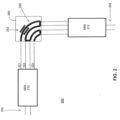
- FIG. 1 is an illustration of an athermal optical device according to an embodiment of the invention.
- Optical device 100 is shown to be an AMZI including input ports 102, output ports 104, and multi-mode interference (MMI) couplers 106 and 108.
- MMI multi-mode interference
- a waveguide propagation section is defined as the region between the input and output ports where there is more than one waveguide, and the waveguides have different delays/optical path lengths.
- the output port such as output ports 104
- light from different waveguides in the waveguide propagation section have undergone interference - for example with an MMI (such as MMIs 106 and 108) or a star coupler.
- MMI multi-mode interference
- waveguides 110 and 112 in the waveguide propagation section each have differing lengths, wherein waveguide 110 is longer than waveguide 112.
- the waveguide cross sections do not necessarily vary in the waveguide propagation section; however, other embodiments described below do utilize varying waveguide cross sections in both dimensions and thermo-optic coefficients (dn/dT).
- said waveguides are to be heated differently.
- the spectrum may be changed in a manner in which different waveguides would be heated separately in order to correct their individual phase errors (e.g., local fabrication errors).
- a single heater may be used to shift the spectrum to correct the deviation.
- a section of waveguide 110 is heated to fixed temperature T set which is greater than the ambient temperature of AMZI 100, T amb .
- the region of AMZI 100 subjected to the ambient temperature is shown as region 122.
- the length of the waveguide section included in heated region 120 is the difference in lengths between waveguide 110 and waveguide 112. In other words, the lengths of each waveguide which are affected by changes in T amb (shown as length 130) are equal, and the section of waveguide 110 included in heated region 120 does not experience any variations in optical path length with variations in T amb .
- the amplitude transmission characteristic of AMZI 100 is athermal and is thus not restricted to operate within a narrow temperature range as are prior art optical devices.
- region 120 of AMZI 100 represents a boundary line with low thermal conductivity.
- the effect of the design of AMZI 100 having heated region 120 is to improve power efficiency, increase temperature uniformity in the T set region, and minimize the heating of region 122.
- This may be achieved in a silicon-on-insulator (SOI) platform, for example, by etching a groove in the top silicon to remove a thermal conduction path between the T set region and T amb region. Additionally the substrates could be etched to remove thermal conduction paths.
- SOI silicon-on-insulator
- the outline of region 120 may represent the edge of a region of uniformly high thermal conductivity to improve the uniformity of the temperature in the T set region. This may be achieved by depositing a high thermal conductivity material above the top cladding (e.g., replace SiO 2 with diamond), by thinning the cladding or BOX and placing a conductor in close proximity to the waveguide, or by removing the substrate and depositing a high thermal conductivity material below the bottom cladding. In either of these implementations the high thermal conductivity material may connect directly to the waveguide layer using thermal shunts.
- a high thermal conductivity material above the top cladding e.g., replace SiO 2 with diamond
- the high thermal conductivity material may connect directly to the waveguide layer using thermal shunts.
- AMZI filter 100 (or a single stage thereof) contains a waveguide propagation section with more than one waveguide, and the waveguides are of different lengths.
- the waveguide propagation region is selectively heated, so that a given waveguide (i.e., waveguide 110) can be divided into a fraction that is at the ambient temperature (T amb ) and a fraction that is at the fixed temperature (T set ).
- the heated regions are chosen such that each waveguide has an equal length that is at temperature T amb , and any remaining length is at T set .
- each waveguide in response to a fluctuation in T amb , each waveguide has an identical change in the effective optical length, and the output frequency spectrum remains unchanged.
- the size of the heated region can be very small, making the technique power-efficient.
- varying T set may linearly shift the frequency spectrum of the filter. This property is useful both to intentionally modify the filter's frequency spectrum and to correct for deviations between the fabricated device and its pre-fabricated design.
- waveguides in the waveguide propagation section are referred to numerically as 1, 2 ... n, and the waveguide number is a variable 'w'.
- the waveguides' lengths are given by L(w).
- the effective index of the optical mode at position 'x' along a waveguide is n eff (w,x).
- the change in index with change in temperature (dn eff /dT) at position 'x' along a waveguide is dn dT w x .
- An athermal FIR filter may comprise waveguides that are subdivided into a fixed temperature (i.e., heated) region and an ambient region, as shown in FIG. 1 .
- L A (1) L A (2). Since the lengths of each waveguide in the waveguide propagation region at the ambient temperature are the same, when the ambient temperature changes, the optical path length of each waveguide changes the same amount, and the differences in length between the waveguides do not change. Therefore, an ambient temperature change may cause a slight time or phase delay in the overall transfer function of the filter but there is no change in the frequency spectrum of the transfer function.
- FIG. 2 is an illustration of an athermal optical device utilizing more than two waveguides according to an embodiment of the invention.
- FIR device 200 is illustrated as implementing an active technique to achieve athermicity in an FIR filter with more than two waveguides.
- Device 200 is shown to include two input ports 202 and two output ports 204.
- MMI 210 is coupled to said input ports to achieve mode transformation and interference.
- MMI 210 may be replaced by other interferometric components, such as one or more Y-junctions, one or more directional couplers, or a star coupler.
- a waveguide propagation section comprising waveguides 221-22n follows MMI 210, in which the different waveguides have different effective optical path lengths.
- MMI 212 follows said waveguide propagation section to achieve mode transformation and interference; output ports 204 follow MMI 212.
- MMI 212 could also be replaced with another interferometric component.
- one or more heaters 250 are used to heat part of the waveguide propagation region to a fixed temperature T set , shown as region 260.
- T set a fixed temperature
- the rest of said waveguide propagation section is subject to the surrounding ambient temperature.
- the cross section of the waveguide in the ambient region is constant, and as shown in this illustration, the length of the waveguide region at the ambient temperature is the same in each of the waveguides.
- heating element 250 comprises a single heating element used to heat each of waveguides 221-22n.
- This heating element may be, for example, a "snake-shaped" thin film resistor that runs along the length of several waveguides to be heated.
- Two potential locations of resistive thermal device (RTD) 252 for heat sensing are shown in this illustration. One location is between the traces of the thin film resistor (i.e., heating element 250). Another location is adjacent to the resistor but close enough that the temperature at the RTD is very close to the temperature of the resistor.
- RTD resistive thermal device
- the thermal gradient across device 200 at steady state is a function of T set and T amb .
- Embodiments of the invention further enable a linear shift in the spectrum of the transfer function of the filter by changing temperature T set .
- the teachings of this description are related to a single filter stage but could be applied to a filter with multiple stages.
- the mathematical analysis describes the response at a single output port to an input in a single input port, but can be extended to simultaneous inputs to different input ports.
- An FIR filter implemented in a PIC may be understood to split and/or interfere input modes from one or more input ports, propagate several modes through different time-delay paths in the waveguide propagation section, and then combine these modes through interference at one or more output ports.
- the input signal is split into waveguides numbered 1 through n, and the time delay to propagate through each waveguide is represented by d w .
- the complex amplitude corresponding to each waveguide is represented by c k,l,w .
- Representation of the filter's response as an impulse response function permits a description of the filter's transmission frequency spectrum. This is found by taking a Fourier transform of h k,l (t) , which will be written as H k,l ( ⁇ ). Representation of the transmission frequency spectrum in this way permits a mathematical description of how changing the heating profile of the waveguides changes the spectrum.
- the frequency spectrum after change in T set may be expressed in terms of H k,l ( ⁇ ) using the well-known Fourier transform properties, shown here for a function in time f(t) and its Fourier transform F( ⁇ ):
- Time shift property: f(t-t 0 ) corresponds to F ⁇ e ⁇ j ⁇ t 0
- the frequency spectrum of the transfer function after change in T set is: 1 s H k , l ⁇ s e j ⁇ t 0 1 ⁇ 1 s
- This function represents a scaling in the width of the entire frequency spectrum. Because the shift in center frequency is small compared to the carrier frequency, this spectral shift may typically be indistinguishable from a linear shift of the entire frequency spectrum, in the wavelength range of interest.
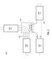
- FIG. 3 illustrates two optical devices sharing a common heated region according to an embodiment of the invention.
- device 300 includes MMI 302 and 304, coupled via waveguide propagation section 306;
- device 310 includes MMI 312 and 314, coupled via waveguides 316 and 318.
- sections of waveguide propagation section 306 are heated in a manner similar to the example embodiment of FIG. 2 (i.e., wherein the waveguides of waveguide propagation section 306 have variable section lengths to be heated, and equal section lengths subject to the ambient temperature).
- Waveguide 316 includes a portion to be heated to a constant temperature, similar to the embodiment of FIG. 1 .
- devices 300 and 310 both utilize region 350, which is heated to a constant temperature (i.e., greater than the ambient temperature).
- the heating of region 350 may be accomplished by using a single thin film electrode that covers the length of all of the waveguides within said region.
- said constant temperature region may be implemented with the use of regions of high and/or low thermal conductivity to make the temperature in the T set region uniform, thereby avoiding heating the T amb region and improving power efficiency. This implementation allows the heater, RTD, heater driver circuit, and feedback control circuit to be shared between two or more FIR filter devices or stages in an FIR filter.
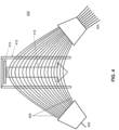
- FIG. 4 is an illustration of an athermal device including a region of low thermal conductivity according to an embodiment of the invention.
- device 400 includes input port 402 and output port 404 coupled via waveguides 406.
- Device 400 utilizes heater 410 set at a fixed temperature to achieve athermal behavior.
- a region of low thermal conductivity, shown as region 412, is used to control the thermal gradient between heater 410 and the ambient region (i.e., the region outside of region 412).
- the low thermal conductivity of region 412 may be achieved, for example, by etching away the waveguide slab region between waveguides. Additionally a thermally conductive substrate may be removed in this region.
- the direction of the generated thermal gradient (shown in this example by directional arrow 414) corresponds to a change in temperature with distance that is roughly linear.
- T w ,x a w ,x ⁇ T amb + b w ,x ⁇ T set
- a(w,x) is the fractional weight of the ambient temperature
- b(w,x) is the fractional weight of the set temperature.
- a waveguide may thus be described as being subdivided into effective lengths that are at the fixed and ambient temperatures, which may be different from the lengths which are and are not covered by a heating element:
- L A w ⁇ 0 L w a w x ⁇ dx
- L H w ⁇ 0 L w b w x ⁇ dx
- each waveguide that is heated to the heater temperature may change by a constant length between each adjacent waveguide, allowing the condition for athermicity to be satisfied.
- This embodiment demonstrates that not only can the shape of the heater or heated region be designed to heat different lengths of each waveguide in an FIR filter, but the thermal gradient can also be engineered so that the effective length of the heated region of each waveguide is correct to achieve athermal behavior.
- L A (k) L A (l) for any k and 1.
- This method embodiment works in the presence of a thermal gradient since the waveguide can be subdivided into an effective length at the ambient temperature and an effective length at the heated temperature, and because these effective lengths do not change as a function of the ambient and fixed temperatures.
- PICs may also utilize passively athermal FIR filters using waveguide regions with different effective thermo-optic coefficients dn/dT and heating a selected area of the PIC.
- passively athermal FIR filters using waveguide regions with different effective thermo-optic coefficients dn/dT and heating a selected area of the PIC.
- the frequency spectrum of the FIR filter linearly shifts, despite its athermicity, in the presence of global ambient temperature changes. Shifting the frequency spectrum can accomplish both active tuning of the filter characteristic and correction of deviations of the fabricated device from design. Using this technique, neither monitoring of temperatures on the chip nor feedback during heater operation is necessary.
- FIG. 5 is an illustration of an optical device for athermal operation and frequency spectrum tuning according to an embodiment of the invention.
- device 500 includes MMI 502 and MMI 504, coupled via waveguides 510 and 520; said waveguides comprise more than one value of dn/dT, either through differing materials or differing waveguide dimensions.
- a heater is used for active tuning, constant power dissipation may be used such that the heated region is raised to T amb +T off , where T off is a function of heater power dissipation. Measurement of temperatures on the chip may not necessary for this embodiment; said active tuning can be used to compensate for fabrication variations or to intentionally shift the spectrum of device 500.
- one of either waveguide sections 512 or 522 comprises a region having a differing dn/dT value, either through differing materials or differing waveguide dimensions, compared to the rest of waveguides 510 or 520, respectively.
- One of either waveguide sections 512 or 522 may also function as an active tuning section through the use of a heater.
- waveguide section 512 may comprise a region having a higher dn/dT value compared to the rest of waveguide 510 while waveguide section 522 comprises a heater, or vice-versa.
- waveguide section 512 may comprise a both a region having a higher dn/dT value compared to the rest of waveguide 510 and a heater either overlapping or in sequence with said waveguide section (e.g., said high dn/dT region and said heater are placed in series), while waveguide section 522 comprises a normal waveguide (i.e., a passive waveguide comprising the same dn/dT value as the "low" dn/dT region of waveguide 510), or vice-versa.
- a normal waveguide i.e., a passive waveguide comprising the same dn/dT value as the "low" dn/dT region of waveguide 510
- embodiments of the invention may further utilize passively athermal FIR filters having waveguide regions with different values of dn eff/ dT in combination with heating a selected area of the device.
- Changing the power dissipated by the localized heater linearly shifts the frequency spectrum of the FIR filter, despite its athermal design (i.e., athermicity in the presence of global ambient temperature changes due to the varying dn eff /dT materials used). Shifting the frequency spectrum can accomplish both active tuning of the filter characteristic and correction of deviations of the fabricated device from design.
- the shift of the frequency spectrum is determined by the offset temperature, which may be set without the need for feedback, as it is proportional to the power dissipated in the heater. Since resistance of the heater does not vary strongly with temperature, the heater setpoint may be set with a constant current or constant voltage source. This technique may reduce power dissipation in comparison to the previously described embodiments, as heating is not required to achieve athermal operation but only to shift the frequency spectrum of the device. Some embodiments of the invention are further configured to heat a region within the high dn/dT waveguide cross section to maximize the energy efficiency of tuning.
- an FIR filter may use waveguide cross sections with differing effective thermo-optic coefficients (dn/dT).
- embodiments of the invention may further use a heater to heat a region of the waveguide propagation section for frequency spectrum tuning.
- the temperature of said heated region is T amb +T off .
- the thermal gradient in the vicinity of the heater may be described by b(w,x), where 0 ⁇ b ( w , x ) ⁇ 1.
- the equation may be satisfied by any combination of heaters - e.g., a single heater of any length on one of the two waveguides.
- the length of the heated region between adjacent waveguides may also have a constant linear increment.
- the heated region can therefore be wedge-shaped as shown in FIG 6A-6C and described in further detail below.
- This function represents a scaling in the width of the entire frequency spectrum.
- the shift in spectrum is entirely a function of the temperature offset from ambient and not a function of the ambient temperature, control of the transmission spectrum of the filter may be achieved without feedback.
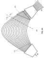
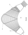
- FIG. 6A - FIG. 6C are illustrations of athermal optical devices for frequency spectrum tuning according to embodiments of the invention. These embodiments describe PICs utilizing heating elements in combination with athermal FIR filters using waveguide regions with different values of dn eff /dT.
- FIG. 6A illustrates device 600 having input port 602 and output ports 604 coupled via plurality of waveguides 610.
- waveguides 610 are comprised two waveguide segment regions - low dn/dT region 612 and high dn/dT region 614, which is shown to include heated region 616.
- the waveguide segments of region 614 are also shown to be shorter in length than the waveguide segments of region 612.
- the shift of the frequency spectrum is determined by the offset temperature, which may be set without the need for feedback, since it is proportional to the power dissipated in the heater. Since resistance of the heater does not vary strongly with temperature, the heater setpoint may be set with a constant current or constant voltage source. This technique may reduce power dissipation in comparison to the previously described embodiments as heating is not required to achieve athermal operation but only to shift the frequency spectrum of the device. Heating a region within high dn/dT region 614 may also maximize the energy efficiency of tuning.
- thermo-optic coefficients (dn/dT) due to changes in the waveguide cross section
- the athermicity condition may be stated as the equality between the change in optical path lengths per unit change in temperature for different waveguides.
- FIG. 6A shows an AWG using regions with more than one waveguide cross section.
- the waveguide types may differ in refractive index n and in dn/dT.
- region 612 By using a region with a lower dn/dT for the majority of the waveguide propagation section (i.e., region 612), the total phase change along a waveguide with change in temperature is reduced.
- region 616 By using a region with higher dn/dT for the T set region (i.e., region 616), a smaller region needs to be heated to compensate for changes in T amb .
- the length that is to be heated is reduced by a factor of (dn/dT) high / (dn/dT) low compared to the length that would be heated if the entire device were made from the waveguide cross section with (dn/dT) low .
- FIG. 6B illustrates device 620 having input port 622 and output ports 624 coupled via plurality of waveguides 630.
- waveguides 630 are materials having different thermo-optic coefficients (dn/dT);; as shown in this illustration, a wedge-shaped region in the middle of device 620, shown as region 632, has a lower dn/dT value than the rest of the waveguide propagation region.
- the shape of region 632 is chosen to fulfill the condition for passive athermicity.
- a heater region 634 is disposed in or near the higher dn/dT region to improve the energy-efficiency of any desired spectral tuning.
- FIG. 6C illustrates another variant of a passively athermal optical device with active tuning.
- Device 640 is shown as having input port 642 and output ports 644 coupled via plurality of waveguides 650.
- wedge-shaped region 652 includes segments of waveguides 650 that have a higher dn/dT value than the rest of the waveguide segments of propagation region 650.
- the heated region is coincident with high dn/dT wedge-shaped region 652 so the spectral tuning may be energy-efficient.
- the wedge shape is defined by the passive athermicity condition where the relative lengths of the waveguides with differing dn/dT are chosen to maintain a relative phase difference between adjacent waveguides with temperature fluctuation.
- the above described embodiments of the invention may comprise SOI or silicon based (e.g., silicon nitride (SiN)) devices, or may comprise devices formed from both silicon and a non-silicon material.
- Said non-silicon material (alternatively referred to as "heterogeneous material”) may comprise one of III-V material, magneto-optic material, or crystal substrate material.
- III-V semiconductors have elements that are found in group III and group V of the periodic table (e.g., Indium Gallium Arsenide Phosphide (InGaAsP), Gallium Indium Arsenide Nitride (GaInAsN)).
- the carrier dispersion effects of III-V based materials may be significantly higher than in silicon based materials, as electron speed in III-V semiconductors is much faster than that in silicon.
- III-V materials have a direct bandgap which enables efficient creation of light from electrical pumping.
- III-V semiconductor materials enable photonic operations with an increased efficiency over silicon for both generating light and modulating the refractive index of light.
- III-V semiconductor materials enable photonic operation with an increased efficiency at generating light from electricity and converting light back into electricity.
- the low optical loss and high quality oxides of silicon are thus combined with the electro-optic efficiency of III-V semiconductors in the heterogeneous optical devices described below; in embodiments of the invention, said heterogeneous devices utilize low loss heterogeneous optical waveguide transitions between the devices' heterogeneous and silicon-only waveguides.
- Magneto-optic materials allow heterogeneous PICs to operate based on the magneto-optic (MO) effect.
- Such devices may devices utilize the Faraday Effect, in which the magnetic field associated with an electrical signal modulates an optical beam, offering high bandwidth modulation, and rotates the electric field of the optical mode enabling optical isolators.
- Said magneto-optic materials may comprise, for example, materials such as such as iron, cobalt, or yttrium iron garnet (YIG).
- Crystal substrate materials provide heterogeneous PICs with a high electromechanical coupling linear electro optic coefficient, low transmission loss, and stable physical and chemical properties.
- Said crystal substrate materials may comprise, for example, lithium niobate (LiNbO3) or lithium tantalate (LiTaO3).
Landscapes
- Physics & Mathematics (AREA)
- Nonlinear Science (AREA)
- General Physics & Mathematics (AREA)
- Optics & Photonics (AREA)
- Engineering & Computer Science (AREA)
- Microelectronics & Electronic Packaging (AREA)
- Optical Modulation, Optical Deflection, Nonlinear Optics, Optical Demodulation, Optical Logic Elements (AREA)
- Optical Integrated Circuits (AREA)
Claims (15)
- Halbleiter-Interferometerfilter (100), das Folgendes umfasst:einen Eingangskoppler (106), um einfallendes Licht aufzunehmen und Teilungslicht, das mehrere Strahlen umfasst, zu erzeugen;einen Ausgangskoppler (108), um die mehreren Strahlen zu kombinieren, um zur Interferenz gebrachtes Licht zu erzeugen;einen ersten Wellenleiter (112), der einen der mehreren Strahlen vom Eingangskoppler zum Ausgangskoppler koppelt, wobei der erste Wellenleiter eine Länge (130) besitzt;einen zweiten Wellenleiter (110), der einen weiteren der mehreren Strahlen vom Eingangskoppler zum Ausgangskoppler koppelt, wobei der zweite Wellenleiter eine verlängerte Länge besitzt, die aufgrund eines Verzögerungspfadabschnitts des zweiten Wellenleiters größer als die Länge des ersten Wellenleiters ist; undeine Heizvorrichtung, die mit dem Verzögerungspfadabschnitt des zweiten Wellenleiters überlappt, um den Verzögerungspfadabschnitt zu einer höheren Temperatur (120) als eine Umgebungstemperatur (122) zu erhitzen, wobei der erste Wellenleiter und ein verbleibender Abschnitt des zweiten Wellenleiters, der sich nicht im Verzögerungspfadabschnitt des zweiten Wellenleiters befindet, bei der Umgebungstemperatur sind, wobeidie Länge des Verzögerungspfadabschnitts gleich der Differenz der Längen zwischen dem ersten Wellenleiter und dem zweiten Wellenleiter ist.
- Halbleiter-Interferometerfilter nach Anspruch 1, wobei der Pfadverzögerungsabschnitt von einem verbleibenden Abschnitt der verlängerten Länge des zweiten Wellenleiters, der im Pfadverzögerungsabschnitt nicht enthalten ist, thermisch isoliert ist.
- Halbleiter-Interferometerfilter nach einem vorhergehenden Anspruch, wobei der Pfadverzögerungsabschnitt ferner vom ersten Wellenleiter thermisch isoliert ist.
- Halbleiter-Interferometerfilter nach einem vorhergehenden Anspruch, wobei das Halbleiter-Interferometerfilter ein Halbleiter-Mach-Zehnder-Interferometerfilter, Halbleiter-MZI-Filter, ist.
- Halbleiter-Interferometerfilter nach einem vorhergehenden Anspruch, wobei die Heizvorrichtung eine Frequenz des zur Interferenz gebrachten Lichts, das durch den Ausgangskoppler ausgegeben wird, ändert.
- Halbleiter-Interferometerfilter nach einem vorhergehenden Anspruch, wobei die Heizvorrichtung durch eine Temperatursteuereinheit gesteuert wird.
- Halbleiter-Interferometerfilter nach Anspruch 6, wobei die Temperatursteuereinheit konfiguriert ist, eine Frequenz des zur Interferenz gebrachten Lichts durch Einstellen einer Leistungsmenge, die durch die Heizvorrichtung abgeleitet wird, abzustimmen.
- Halbleiter-Interferometerfilter nach Anspruch 6 oder Anspruch 7, das ferner einen Temperatursensor umfasst, der konfiguriert ist, eine Temperatur des Verzögerungspfadabschnitts des zweiten Wellenleiters zu erfassen.
- Halbleiter-Interferometerfilter nach Anspruch 8, wobei die Temperatursteuereinheit konfiguriert ist, eine Frequenz des zur Interferenz gebrachten Lichts in Reaktion auf einen Temperaturwert, der durch den Temperatursensor erzeugt wird, abzustimmen.
- Verfahren zum Abstimmen eines Halbleiter-Interferometerfilters (100), wobei das Verfahren Folgendes umfasst:Teilen durch einen Eingangskoppler (106) von einfallendem Licht in einen ersten Wellenleiter (112) und einen zweiten Wellenleiter (110), wobei der erste Wellenleiter eine Länge (130) besitzt und der zweite Wellenleiter eine verlängerte Länge besitzt, die aufgrund eines Verzögerungspfadabschnitts des zweiten Wellenleiters größer als die Länge des ersten Wellenleiters ist;Erhitzen unter Verwendung einer Heizvorrichtung (250) des Halbleiter-Interferometerfilters, die mit dem Verzögerungspfadabschnitt des zweiten Wellenleiters überlappt, des Verzögerungspfadabschnitts zu einer höheren Temperatur (120) als eine Umgebungstemperatur (122), wobei der erste Wellenleiter und ein verbleibender Abschnitt des zweiten Wellenleiters, der sich nicht im Verzögerungspfadabschnitt des zweiten Wellenleiters befindet, auf Umgebungstemperatur sind, wobei
die Länge des Verzögerungspfadabschnitts gleich der Differenz der Längen zwischen dem ersten Wellenleiter und dem zweiten Wellenleiter ist; undBringen zur Interferenz durch einen Ausgangskoppler (108) von Licht von dem ersten Wellenleiter und dem zweiten Wellenleiter, um zur Interferenz gebrachtes Licht zu erzeugen. - Verfahren nach Anspruch 10, wobei der Pfadverzögerungsabschnitt von einem verbleibenden Abschnitt der verlängerten Länge des zweiten Wellenleiters, der im Pfadverzögerungsabschnitt nicht enthalten ist, thermisch isoliert ist.
- Verfahren nach einem der Ansprüche 10-11, wobei der Pfadverzögerungsabschnitt ferner vom ersten Wellenleiter thermisch isoliert ist.
- Verfahren nach einem der Ansprüche 10-12, wobei das Halbleiter-Interferometerfilter ein Halbleiter-Mach-Zehnder-Interferometerfilter, Halbleiter-MZI-Filter, ist.
- Verfahren nach einem der Ansprüche 10-13, wobei die Heizvorrichtung eine Frequenz des zur Interferenz gebrachten Lichts, das durch den Ausgangskoppler ausgegeben wird, ändert.
- Verfahren nach einem der Ansprüche 10-14, wobei die Heizvorrichtung durch eine Temperatursteuereinheit gesteuert wird.
Applications Claiming Priority (3)
| Application Number | Priority Date | Filing Date | Title |
|---|---|---|---|
| US13/751,492 US9207399B2 (en) | 2013-01-28 | 2013-01-28 | Athermal optical filter with active tuning and simplified control |
| EP19216676.7A EP3650895B1 (de) | 2013-01-28 | 2014-01-28 | Einstellbarer temperaturunverändenlicher optischer filter mit vereinfachter steuerbarkeit |
| EP14000296.5A EP2759857B1 (de) | 2013-01-28 | 2014-01-28 | Athermischer optischer Filter mit aktiver Abstimmung und vereinfachter Steuerung |
Related Parent Applications (2)
| Application Number | Title | Priority Date | Filing Date |
|---|---|---|---|
| EP19216676.7A Division EP3650895B1 (de) | 2013-01-28 | 2014-01-28 | Einstellbarer temperaturunverändenlicher optischer filter mit vereinfachter steuerbarkeit |
| EP14000296.5A Division EP2759857B1 (de) | 2013-01-28 | 2014-01-28 | Athermischer optischer Filter mit aktiver Abstimmung und vereinfachter Steuerung |
Publications (3)
| Publication Number | Publication Date |
|---|---|
| EP3958032A1 EP3958032A1 (de) | 2022-02-23 |
| EP3958032B1 true EP3958032B1 (de) | 2023-11-01 |
| EP3958032C0 EP3958032C0 (de) | 2023-11-01 |
Family
ID=50064362
Family Applications (3)
| Application Number | Title | Priority Date | Filing Date |
|---|---|---|---|
| EP21199538.6A Active EP3958032B1 (de) | 2013-01-28 | 2014-01-28 | Athermischer optischer filter mit aktiver abstimmung und vereinfachter steuerung |
| EP14000296.5A Active EP2759857B1 (de) | 2013-01-28 | 2014-01-28 | Athermischer optischer Filter mit aktiver Abstimmung und vereinfachter Steuerung |
| EP19216676.7A Active EP3650895B1 (de) | 2013-01-28 | 2014-01-28 | Einstellbarer temperaturunverändenlicher optischer filter mit vereinfachter steuerbarkeit |
Family Applications After (2)
| Application Number | Title | Priority Date | Filing Date |
|---|---|---|---|
| EP14000296.5A Active EP2759857B1 (de) | 2013-01-28 | 2014-01-28 | Athermischer optischer Filter mit aktiver Abstimmung und vereinfachter Steuerung |
| EP19216676.7A Active EP3650895B1 (de) | 2013-01-28 | 2014-01-28 | Einstellbarer temperaturunverändenlicher optischer filter mit vereinfachter steuerbarkeit |
Country Status (2)
| Country | Link |
|---|---|
| US (4) | US9207399B2 (de) |
| EP (3) | EP3958032B1 (de) |
Families Citing this family (13)
| Publication number | Priority date | Publication date | Assignee | Title |
|---|---|---|---|---|
| US9207399B2 (en) | 2013-01-28 | 2015-12-08 | Aurrion, Inc. | Athermal optical filter with active tuning and simplified control |
| JP6273701B2 (ja) * | 2013-06-27 | 2018-02-07 | 住友電気工業株式会社 | 光半導体素子 |
| US10281648B2 (en) * | 2013-07-30 | 2019-05-07 | President And Fellows Of Harvard College | Device support structures from bulk substrates |
| US9685762B1 (en) * | 2014-09-30 | 2017-06-20 | Aurrion, Inc. | Semiconductor optical amplifier with gain flattening filter |
| EP3929654B1 (de) | 2015-07-24 | 2025-06-18 | OpenLight Photonics, Inc. | Phasenabstimmung in wellenleiter-arrays |
| JP6759739B2 (ja) * | 2016-06-13 | 2020-09-23 | 富士通オプティカルコンポーネンツ株式会社 | 光デバイス、波長可変光源、及びこれを用いた光送信器 |
| GB2551968A (en) * | 2016-06-28 | 2018-01-10 | Oclaro Tech Ltd | Optical locker |
| US9964703B2 (en) * | 2016-10-10 | 2018-05-08 | Juniper Networks, Inc. | Integrated wavelength locker |
| US10128634B2 (en) | 2016-10-10 | 2018-11-13 | Juniper Networks, Inc. | Integrated wavelength locker |
| US10488589B2 (en) * | 2017-02-08 | 2019-11-26 | Rockley Photonics Limited | T-shaped arrayed waveguide grating |
| CN110582710A (zh) | 2017-07-17 | 2019-12-17 | 洛克利光子有限公司 | 无热化多路径干涉滤波器 |
| US12143156B2 (en) | 2021-01-08 | 2024-11-12 | Rockwell Collins, Inc. | Multi-point self-calibration for broadband optical sensor interrogator |
| CN114018837B (zh) * | 2021-10-11 | 2024-08-13 | 吉林大学第一医院 | 基于硅波导主流法监测人体呼出水蒸气和二氧化碳气体的传感器 |
Family Cites Families (59)
| Publication number | Priority date | Publication date | Assignee | Title |
|---|---|---|---|---|
| BE480697A (de) | 1960-11-02 | |||
| FR2660439B1 (fr) | 1990-03-27 | 1993-06-04 | Thomson Csf | Structure guidante integree en trois dimensions et son procede de realisation. |
| US5617234A (en) * | 1994-09-26 | 1997-04-01 | Nippon Telegraph & Telephone Corporation | Multiwavelength simultaneous monitoring circuit employing arrayed-waveguide grating |
| US5701371A (en) | 1994-10-31 | 1997-12-23 | Nippon Telegraph And Telephone Corporation | Tunable optical filter |
| KR100274804B1 (ko) | 1998-04-22 | 2001-01-15 | 윤종용 | 양방향 광파장 다중화기/분할기 |
| JP3527431B2 (ja) | 1999-03-01 | 2004-05-17 | 日本電信電話株式会社 | アレイ光導波路熱光学位相シフタ,アレイ光導波路格子波長可変フィルタおよびアレイ光導波路光スイッチ |
| US6421478B1 (en) | 1999-05-11 | 2002-07-16 | Jds Fitel Inc. | Tapered MMI coupler |
| DE69938132T2 (de) | 1999-09-28 | 2009-03-05 | Corning Incorporated | Athermischer Wellenleitergitter-Multiplexer (AWG) mit Polymersegment, sowie entsprechendes Herstellungsverfahren |
| US6289147B1 (en) | 1999-11-01 | 2001-09-11 | Bbv Design Bv | Passband flattening of a phasar |
| US6243517B1 (en) * | 1999-11-04 | 2001-06-05 | Sparkolor Corporation | Channel-switched cross-connect |
| US6466707B1 (en) | 2000-08-21 | 2002-10-15 | Corning Incorporated | Phasar athermalization using a slab waveguide |
| DE10102460B4 (de) * | 2001-01-15 | 2011-03-17 | Finisar Corp., Sunnyvale | Anordnungen und Verfahren zur kanalabhängigen Abschwächung der Pegel einer Mehrzahl optischer Datenkanäle |
| JP3703013B2 (ja) | 2001-01-26 | 2005-10-05 | 日本電信電話株式会社 | 干渉計光回路及びその製造方法 |
| US6853773B2 (en) | 2001-04-30 | 2005-02-08 | Kotusa, Inc. | Tunable filter |
| JP2003035830A (ja) | 2001-05-15 | 2003-02-07 | Furukawa Electric Co Ltd:The | 光波長合分波器 |
| EP1279999A1 (de) * | 2001-07-23 | 2003-01-29 | Corning Incorporated | Polarisationsunabhängiger optischer Dämpfungsregler |
| JP2003131051A (ja) * | 2001-08-16 | 2003-05-08 | Nec Corp | 光デバイス |
| US6816636B2 (en) | 2001-09-12 | 2004-11-09 | Honeywell International Inc. | Tunable optical filter |
| GB2380342B (en) | 2001-09-28 | 2005-08-10 | Fujitsu Network Comm Inc | A compensator for polarisation-mode dispersion compensation |
| KR100908623B1 (ko) | 2001-10-30 | 2009-07-21 | 호야 코포레이션 유에스에이 | 광출력의 횡단 전달을 이용하는 광학적 접합 장치 및 방법 |
| US6872985B2 (en) | 2001-11-15 | 2005-03-29 | Hrl Laboratories, Llc | Waveguide-bonded optoelectronic devices |
| AU2002365565A1 (en) | 2001-11-23 | 2003-06-10 | Xponent Photonics Inc. | Alignment apparatus and methods for transverse optical coupling |
| EP1319967A1 (de) | 2001-12-13 | 2003-06-18 | Alcatel | Temperaturunabhängiges Wellenleitergitter (AWG), mit thermischer Kompensation im Schichtwellenleiterbereich |
| JP3884341B2 (ja) | 2002-01-21 | 2007-02-21 | 古河電気工業株式会社 | 可変分散補償器およびその可変分散補償器を用いた可変分散補償デバイス |
| US6816665B2 (en) | 2002-05-09 | 2004-11-09 | Lynx Photonic Networks Inc. | Constant power operation thermo-optic switch |
| US7194176B2 (en) * | 2002-05-29 | 2007-03-20 | Hoya Corporation | Functional optical devices and methods for producing them |
| US7305162B2 (en) | 2002-05-30 | 2007-12-04 | Intel Corporation | Reducing the temperature sensitivity of optical waveguide interference filters |
| GB0214085D0 (en) * | 2002-06-19 | 2002-07-31 | Alcatel Optronics Uk Ltd | Athermal arrayed waveguide grating |
| US7085438B2 (en) | 2002-12-06 | 2006-08-01 | Nippon Telegraph And Telephone Corporation | Optical multi/demultiplexing circuit equipped with phase generating device |
| US7095920B1 (en) | 2003-02-11 | 2006-08-22 | Little Optics Inc | Broadband optical via |
| US6978056B2 (en) * | 2003-06-04 | 2005-12-20 | Covega, Inc. | Waveguide modulators having bias control with reduced temperature dependence |
| JP2005156855A (ja) * | 2003-11-25 | 2005-06-16 | Nec Corp | 多チャンネルマッハツェンダ干渉計型光回路 |
| US7447393B2 (en) * | 2004-01-16 | 2008-11-04 | Neophotonics Corporation | Thermal control of optical components |
| US7061596B2 (en) | 2004-08-19 | 2006-06-13 | Lucent Technologies Inc. | Wavelength-tracking dispersion compensator |
| US7161726B2 (en) * | 2004-11-05 | 2007-01-09 | Lumera Corporation | Linear optical modulators and method of linear optical modulation |
| CA2499651A1 (en) * | 2005-03-04 | 2006-09-04 | Itf Technologies Optiques Inc./Itf Optical Technologies Inc. | All-fiber phase controlled delay interferometer and method of making the same |
| US7343066B2 (en) * | 2005-08-16 | 2008-03-11 | Lucent Technologies Inc. | Reconfigurable optical add/drop multiplexer |
| US7231113B2 (en) | 2005-08-19 | 2007-06-12 | Infinera Corporation | Coupled optical waveguide resonators with heaters for thermo-optic control of wavelength and compound filter shape |
| US8207509B2 (en) * | 2006-09-01 | 2012-06-26 | Pacific Biosciences Of California, Inc. | Substrates, systems and methods for analyzing materials |
| WO2009113469A1 (ja) * | 2008-03-13 | 2009-09-17 | 日本電気株式会社 | 光デバイス、その製造方法とそれを用いた光集積デバイス |
| US8111729B2 (en) | 2008-03-25 | 2012-02-07 | Intel Corporation | Multi-wavelength hybrid silicon laser array |
| JP5457661B2 (ja) | 2008-07-14 | 2014-04-02 | 日本電信電話株式会社 | 光波長合分波回路 |
| JP5399693B2 (ja) | 2008-07-14 | 2014-01-29 | 日本電信電話株式会社 | 光波長合分波回路 |
| US20100111533A1 (en) | 2008-11-06 | 2010-05-06 | Nortel Networks Limited | Wdm pon system |
| JP2010175645A (ja) | 2009-01-27 | 2010-08-12 | Nippon Telegr & Teleph Corp <Ntt> | 光波長多重信号監視装置および方法 |
| US8611388B2 (en) | 2009-10-13 | 2013-12-17 | Skorpios Technologies, Inc. | Method and system for heterogeneous substrate bonding of waveguide receivers |
| US8457453B2 (en) * | 2009-11-02 | 2013-06-04 | Cornell University | Passively-thermally-stabilized photonic apparatus, method, and applications |
| WO2011132283A1 (ja) * | 2010-04-22 | 2011-10-27 | 富士通株式会社 | 光変調装置、光変調装置の駆動方法、及び光変調装置の製造方法 |
| JP2012014039A (ja) | 2010-07-02 | 2012-01-19 | Furukawa Electric Co Ltd:The | 波長合分波器およびその製造方法 |
| EP2463694A1 (de) | 2010-12-10 | 2012-06-13 | Alcatel Lucent | Laserstruktur mit verteiltem Feedback für eine photonenintegrierte Schaltung und Verfahren zur Herstellung der Struktur |
| US9036954B2 (en) * | 2011-04-01 | 2015-05-19 | Intel Corporation | Optical waveguide structure |
| US8805187B2 (en) * | 2012-03-19 | 2014-08-12 | Neophotonics Corporation | Wavelength router with feedback control comprising optical monitor ports |
| US9525490B2 (en) | 2012-07-26 | 2016-12-20 | Aurrion, Inc. | Reconfigurable optical transmitter |
| US8831049B2 (en) | 2012-09-14 | 2014-09-09 | Laxense Inc. | Tunable optical system with hybrid integrated laser |
| US9207399B2 (en) * | 2013-01-28 | 2015-12-08 | Aurrion, Inc. | Athermal optical filter with active tuning and simplified control |
| US20150124845A1 (en) | 2013-11-06 | 2015-05-07 | Aurrion, Inc. | Optical mode steering for wavelength stabilization |
| US9400402B2 (en) | 2014-01-07 | 2016-07-26 | Electronics And Telecommunications Research Institute | Optical waveguide and optical device based on the same |
| US9553689B2 (en) | 2014-12-12 | 2017-01-24 | Inphi Corporation | Temperature insensitive DEMUX/MUX in silicon photonics |
| EP3929654B1 (de) | 2015-07-24 | 2025-06-18 | OpenLight Photonics, Inc. | Phasenabstimmung in wellenleiter-arrays |
-
2013
- 2013-01-28 US US13/751,492 patent/US9207399B2/en active Active
-
2014
- 2014-01-28 EP EP21199538.6A patent/EP3958032B1/de active Active
- 2014-01-28 EP EP14000296.5A patent/EP2759857B1/de active Active
- 2014-01-28 EP EP19216676.7A patent/EP3650895B1/de active Active
-
2015
- 2015-11-02 US US14/929,603 patent/US9684190B1/en active Active
-
2017
- 2017-06-02 US US15/612,364 patent/US9952455B2/en active Active
-
2018
- 2018-03-15 US US15/922,123 patent/US10151939B2/en active Active
Also Published As
| Publication number | Publication date |
|---|---|
| EP2759857A2 (de) | 2014-07-30 |
| US9684190B1 (en) | 2017-06-20 |
| EP3650895B1 (de) | 2021-09-29 |
| EP3650895A1 (de) | 2020-05-13 |
| US20170269390A1 (en) | 2017-09-21 |
| US20140212092A1 (en) | 2014-07-31 |
| US10151939B2 (en) | 2018-12-11 |
| EP3958032A1 (de) | 2022-02-23 |
| EP2759857B1 (de) | 2019-12-18 |
| US9207399B2 (en) | 2015-12-08 |
| EP3958032C0 (de) | 2023-11-01 |
| US9952455B2 (en) | 2018-04-24 |
| EP2759857A3 (de) | 2018-02-14 |
| US20180217413A1 (en) | 2018-08-02 |
Similar Documents
| Publication | Publication Date | Title |
|---|---|---|
| EP3958032B1 (de) | Athermischer optischer filter mit aktiver abstimmung und vereinfachter steuerung | |
| WO2016184329A1 (en) | Optical phase shifter | |
| USRE48654E1 (en) | Photonic integrated circuit incorporating a bandgap temperature sensor | |
| EP3938822B1 (de) | Polarisationsunabhängige photonische vorrichtung mit multimode-komponente | |
| Mendez-Astudillo et al. | Compact thermo-optic MZI switch in silicon-on-insulator using direct carrier injection | |
| US8923660B2 (en) | System and method for an optical phase shifter | |
| US9513437B2 (en) | Photonic integrated circuit incorporating a bandgap temperature sensor | |
| Melati et al. | Athermal echelle grating filter in silicon-on-insulator using a temperature-synchronized input | |
| Jeong et al. | 1× 4 channel Si-nanowire microring-assisted multiple delayline-based optical MUX/DeMUX | |
| EP2871504A1 (de) | Optische Moduslenkung zur Wellenlängenstabilisierung | |
| US20070212012A1 (en) | Planar Lightwave Circuit Type Variable Optical Attenuator | |
| Lipka et al. | Energy-efficient wavelength multiplexers based on hydrogenated amorphous silicon resonators | |
| Melati et al. | Athermal echelle grating and tunable echelle grating demultiplexers using a Mach-Zehnder interferometer launch structure | |
| Bozeat et al. | Silicon based waveguides | |
| Romero-García et al. | Broadband, temperature tolerant and passively biased resonantly enhanced Mach-Zehnder modulators | |
| JP2012103505A (ja) | 多連熱光学位相シフタおよびそれを用いた光干渉回路 | |
| Moreira | Integrated optical delay line circuits on a ultra-low loss planar waveguide platform | |
| Tunesi et al. | Enhanced Bandwidth Tunability in Thermally Controlled Multi-pitch Contra-directional Couplers | |
| JP3573332B2 (ja) | 干渉型熱光学光部品 | |
| CN101980069B (zh) | 用于波导配置的电光间隙室 | |
| Jiao et al. | Silicon Waveguides and Temperature-Dependent Performance | |
| Hunsperger | Coupling between waveguides | |
| Osgood jr et al. | Optical Couplers | |
| Melati et al. | Temperature-insensitive echelle wavelength demultiplexer on standard silicon-on-insulator platform | |
| Cunha | Silicon Photonics Optical Beamformer for Broadband Phased Array Antennas |
Legal Events
| Date | Code | Title | Description |
|---|---|---|---|
| PUAI | Public reference made under article 153(3) epc to a published international application that has entered the european phase |
Free format text: ORIGINAL CODE: 0009012 |
|
| STAA | Information on the status of an ep patent application or granted ep patent |
Free format text: STATUS: THE APPLICATION HAS BEEN PUBLISHED |
|
| AC | Divisional application: reference to earlier application |
Ref document number: 2759857 Country of ref document: EP Kind code of ref document: P Ref document number: 3650895 Country of ref document: EP Kind code of ref document: P |
|
| AK | Designated contracting states |
Kind code of ref document: A1 Designated state(s): AL AT BE BG CH CY CZ DE DK EE ES FI FR GB GR HR HU IE IS IT LI LT LU LV MC MK MT NL NO PL PT RO RS SE SI SK SM TR |
|
| STAA | Information on the status of an ep patent application or granted ep patent |
Free format text: STATUS: REQUEST FOR EXAMINATION WAS MADE |
|
| RAP3 | Party data changed (applicant data changed or rights of an application transferred) |
Owner name: OPENLIGHT PHOTONICS, INC. |
|
| 17P | Request for examination filed |
Effective date: 20220823 |
|
| RBV | Designated contracting states (corrected) |
Designated state(s): AL AT BE BG CH CY CZ DE DK EE ES FI FR GB GR HR HU IE IS IT LI LT LU LV MC MK MT NL NO PL PT RO RS SE SI SK SM TR |
|
| GRAP | Despatch of communication of intention to grant a patent |
Free format text: ORIGINAL CODE: EPIDOSNIGR1 |
|
| STAA | Information on the status of an ep patent application or granted ep patent |
Free format text: STATUS: GRANT OF PATENT IS INTENDED |
|
| INTG | Intention to grant announced |
Effective date: 20230525 |
|
| GRAS | Grant fee paid |
Free format text: ORIGINAL CODE: EPIDOSNIGR3 |
|
| GRAA | (expected) grant |
Free format text: ORIGINAL CODE: 0009210 |
|
| STAA | Information on the status of an ep patent application or granted ep patent |
Free format text: STATUS: THE PATENT HAS BEEN GRANTED |
|
| AC | Divisional application: reference to earlier application |
Ref document number: 2759857 Country of ref document: EP Kind code of ref document: P Ref document number: 3650895 Country of ref document: EP Kind code of ref document: P |
|
| AK | Designated contracting states |
Kind code of ref document: B1 Designated state(s): AL AT BE BG CH CY CZ DE DK EE ES FI FR GB GR HR HU IE IS IT LI LT LU LV MC MK MT NL NO PL PT RO RS SE SI SK SM TR |
|
| REG | Reference to a national code |
Ref country code: GB Ref legal event code: FG4D |
|
| REG | Reference to a national code |
Ref country code: CH Ref legal event code: EP |
|
| REG | Reference to a national code |
Ref country code: IE Ref legal event code: FG4D |
|
| REG | Reference to a national code |
Ref country code: DE Ref legal event code: R096 Ref document number: 602014088793 Country of ref document: DE |
|
| U01 | Request for unitary effect filed |
Effective date: 20231201 |
|
| U07 | Unitary effect registered |
Designated state(s): AT BE BG DE DK EE FI FR IT LT LU LV MT NL PT SE SI Effective date: 20231221 |
|
| U20 | Renewal fee for the european patent with unitary effect paid |
Year of fee payment: 11 Effective date: 20240122 |
|
| PG25 | Lapsed in a contracting state [announced via postgrant information from national office to epo] |
Ref country code: GR Free format text: LAPSE BECAUSE OF FAILURE TO SUBMIT A TRANSLATION OF THE DESCRIPTION OR TO PAY THE FEE WITHIN THE PRESCRIBED TIME-LIMIT Effective date: 20240202 |
|
| PG25 | Lapsed in a contracting state [announced via postgrant information from national office to epo] |
Ref country code: IS Free format text: LAPSE BECAUSE OF FAILURE TO SUBMIT A TRANSLATION OF THE DESCRIPTION OR TO PAY THE FEE WITHIN THE PRESCRIBED TIME-LIMIT Effective date: 20240301 |
|
| PG25 | Lapsed in a contracting state [announced via postgrant information from national office to epo] |
Ref country code: ES Free format text: LAPSE BECAUSE OF FAILURE TO SUBMIT A TRANSLATION OF THE DESCRIPTION OR TO PAY THE FEE WITHIN THE PRESCRIBED TIME-LIMIT Effective date: 20231101 |
|
| PG25 | Lapsed in a contracting state [announced via postgrant information from national office to epo] |
Ref country code: IS Free format text: LAPSE BECAUSE OF FAILURE TO SUBMIT A TRANSLATION OF THE DESCRIPTION OR TO PAY THE FEE WITHIN THE PRESCRIBED TIME-LIMIT Effective date: 20240301 Ref country code: GR Free format text: LAPSE BECAUSE OF FAILURE TO SUBMIT A TRANSLATION OF THE DESCRIPTION OR TO PAY THE FEE WITHIN THE PRESCRIBED TIME-LIMIT Effective date: 20240202 Ref country code: ES Free format text: LAPSE BECAUSE OF FAILURE TO SUBMIT A TRANSLATION OF THE DESCRIPTION OR TO PAY THE FEE WITHIN THE PRESCRIBED TIME-LIMIT Effective date: 20231101 |
|
| PG25 | Lapsed in a contracting state [announced via postgrant information from national office to epo] |
Ref country code: RS Free format text: LAPSE BECAUSE OF FAILURE TO SUBMIT A TRANSLATION OF THE DESCRIPTION OR TO PAY THE FEE WITHIN THE PRESCRIBED TIME-LIMIT Effective date: 20231101 Ref country code: PL Free format text: LAPSE BECAUSE OF FAILURE TO SUBMIT A TRANSLATION OF THE DESCRIPTION OR TO PAY THE FEE WITHIN THE PRESCRIBED TIME-LIMIT Effective date: 20231101 Ref country code: NO Free format text: LAPSE BECAUSE OF FAILURE TO SUBMIT A TRANSLATION OF THE DESCRIPTION OR TO PAY THE FEE WITHIN THE PRESCRIBED TIME-LIMIT Effective date: 20240201 Ref country code: HR Free format text: LAPSE BECAUSE OF FAILURE TO SUBMIT A TRANSLATION OF THE DESCRIPTION OR TO PAY THE FEE WITHIN THE PRESCRIBED TIME-LIMIT Effective date: 20231101 |
|
| PG25 | Lapsed in a contracting state [announced via postgrant information from national office to epo] |
Ref country code: CZ Free format text: LAPSE BECAUSE OF FAILURE TO SUBMIT A TRANSLATION OF THE DESCRIPTION OR TO PAY THE FEE WITHIN THE PRESCRIBED TIME-LIMIT Effective date: 20231101 |
|
| PG25 | Lapsed in a contracting state [announced via postgrant information from national office to epo] |
Ref country code: SK Free format text: LAPSE BECAUSE OF FAILURE TO SUBMIT A TRANSLATION OF THE DESCRIPTION OR TO PAY THE FEE WITHIN THE PRESCRIBED TIME-LIMIT Effective date: 20231101 |
|
| PG25 | Lapsed in a contracting state [announced via postgrant information from national office to epo] |
Ref country code: SM Free format text: LAPSE BECAUSE OF FAILURE TO SUBMIT A TRANSLATION OF THE DESCRIPTION OR TO PAY THE FEE WITHIN THE PRESCRIBED TIME-LIMIT Effective date: 20231101 Ref country code: SK Free format text: LAPSE BECAUSE OF FAILURE TO SUBMIT A TRANSLATION OF THE DESCRIPTION OR TO PAY THE FEE WITHIN THE PRESCRIBED TIME-LIMIT Effective date: 20231101 Ref country code: CZ Free format text: LAPSE BECAUSE OF FAILURE TO SUBMIT A TRANSLATION OF THE DESCRIPTION OR TO PAY THE FEE WITHIN THE PRESCRIBED TIME-LIMIT Effective date: 20231101 |
|
| REG | Reference to a national code |
Ref country code: DE Ref legal event code: R097 Ref document number: 602014088793 Country of ref document: DE |
|
| PG25 | Lapsed in a contracting state [announced via postgrant information from national office to epo] |
Ref country code: MC Free format text: LAPSE BECAUSE OF FAILURE TO SUBMIT A TRANSLATION OF THE DESCRIPTION OR TO PAY THE FEE WITHIN THE PRESCRIBED TIME-LIMIT Effective date: 20231101 |
|
| PG25 | Lapsed in a contracting state [announced via postgrant information from national office to epo] |
Ref country code: MC Free format text: LAPSE BECAUSE OF FAILURE TO SUBMIT A TRANSLATION OF THE DESCRIPTION OR TO PAY THE FEE WITHIN THE PRESCRIBED TIME-LIMIT Effective date: 20231101 |
|
| REG | Reference to a national code |
Ref country code: CH Ref legal event code: PL |
|
| PLBE | No opposition filed within time limit |
Free format text: ORIGINAL CODE: 0009261 |
|
| STAA | Information on the status of an ep patent application or granted ep patent |
Free format text: STATUS: NO OPPOSITION FILED WITHIN TIME LIMIT |
|
| 26N | No opposition filed |
Effective date: 20240802 |
|
| PG25 | Lapsed in a contracting state [announced via postgrant information from national office to epo] |
Ref country code: CH Free format text: LAPSE BECAUSE OF NON-PAYMENT OF DUE FEES Effective date: 20240131 |
|
| GBPC | Gb: european patent ceased through non-payment of renewal fee |
Effective date: 20240201 |
|
| PG25 | Lapsed in a contracting state [announced via postgrant information from national office to epo] |
Ref country code: CH Free format text: LAPSE BECAUSE OF NON-PAYMENT OF DUE FEES Effective date: 20240131 |
|
| PG25 | Lapsed in a contracting state [announced via postgrant information from national office to epo] |
Ref country code: GB Free format text: LAPSE BECAUSE OF NON-PAYMENT OF DUE FEES Effective date: 20240201 |
|
| U20 | Renewal fee for the european patent with unitary effect paid |
Year of fee payment: 12 Effective date: 20241213 |
|
| PG25 | Lapsed in a contracting state [announced via postgrant information from national office to epo] |
Ref country code: IE Free format text: LAPSE BECAUSE OF NON-PAYMENT OF DUE FEES Effective date: 20240128 |
|
| PG25 | Lapsed in a contracting state [announced via postgrant information from national office to epo] |
Ref country code: IE Free format text: LAPSE BECAUSE OF NON-PAYMENT OF DUE FEES Effective date: 20240128 Ref country code: GB Free format text: LAPSE BECAUSE OF NON-PAYMENT OF DUE FEES Effective date: 20240201 |
|
| PG25 | Lapsed in a contracting state [announced via postgrant information from national office to epo] |
Ref country code: RO Free format text: LAPSE BECAUSE OF FAILURE TO SUBMIT A TRANSLATION OF THE DESCRIPTION OR TO PAY THE FEE WITHIN THE PRESCRIBED TIME-LIMIT Effective date: 20231101 |
|
| PG25 | Lapsed in a contracting state [announced via postgrant information from national office to epo] |
Ref country code: CY Free format text: LAPSE BECAUSE OF FAILURE TO SUBMIT A TRANSLATION OF THE DESCRIPTION OR TO PAY THE FEE WITHIN THE PRESCRIBED TIME-LIMIT; INVALID AB INITIO Effective date: 20140128 |
|
| PG25 | Lapsed in a contracting state [announced via postgrant information from national office to epo] |
Ref country code: HU Free format text: LAPSE BECAUSE OF FAILURE TO SUBMIT A TRANSLATION OF THE DESCRIPTION OR TO PAY THE FEE WITHIN THE PRESCRIBED TIME-LIMIT; INVALID AB INITIO Effective date: 20140128 |
|
| PG25 | Lapsed in a contracting state [announced via postgrant information from national office to epo] |
Ref country code: TR Free format text: LAPSE BECAUSE OF FAILURE TO SUBMIT A TRANSLATION OF THE DESCRIPTION OR TO PAY THE FEE WITHIN THE PRESCRIBED TIME-LIMIT Effective date: 20231101 |
|
| U20 | Renewal fee for the european patent with unitary effect paid |
Year of fee payment: 13 Effective date: 20251219 |