EP3958314B1 - Structure semi-conductrice et son procédé de fabrication - Google Patents
Structure semi-conductrice et son procédé de fabrication Download PDFInfo
- Publication number
- EP3958314B1 EP3958314B1 EP21800975.1A EP21800975A EP3958314B1 EP 3958314 B1 EP3958314 B1 EP 3958314B1 EP 21800975 A EP21800975 A EP 21800975A EP 3958314 B1 EP3958314 B1 EP 3958314B1
- Authority
- EP
- European Patent Office
- Prior art keywords
- layer
- word line
- substrate
- forming
- line trench
- Prior art date
- Legal status (The legal status is an assumption and is not a legal conclusion. Google has not performed a legal analysis and makes no representation as to the accuracy of the status listed.)
- Active
Links
Images













Classifications
-
- H—ELECTRICITY
- H10—SEMICONDUCTOR DEVICES; ELECTRIC SOLID-STATE DEVICES NOT OTHERWISE PROVIDED FOR
- H10B—ELECTRONIC MEMORY DEVICES
- H10B12/00—Dynamic random access memory [DRAM] devices
- H10B12/30—DRAM devices comprising one-transistor - one-capacitor [1T-1C] memory cells
- H10B12/34—DRAM devices comprising one-transistor - one-capacitor [1T-1C] memory cells the transistor being at least partially in a trench in the substrate
-
- H—ELECTRICITY
- H10—SEMICONDUCTOR DEVICES; ELECTRIC SOLID-STATE DEVICES NOT OTHERWISE PROVIDED FOR
- H10B—ELECTRONIC MEMORY DEVICES
- H10B12/00—Dynamic random access memory [DRAM] devices
- H10B12/01—Manufacture or treatment
- H10B12/02—Manufacture or treatment for one transistor one-capacitor [1T-1C] memory cells
- H10B12/05—Making the transistor
- H10B12/053—Making the transistor the transistor being at least partially in a trench in the substrate
-
- H—ELECTRICITY
- H10—SEMICONDUCTOR DEVICES; ELECTRIC SOLID-STATE DEVICES NOT OTHERWISE PROVIDED FOR
- H10B—ELECTRONIC MEMORY DEVICES
- H10B12/00—Dynamic random access memory [DRAM] devices
- H10B12/30—DRAM devices comprising one-transistor - one-capacitor [1T-1C] memory cells
- H10B12/48—Data lines or contacts therefor
- H10B12/488—Word lines
-
- H—ELECTRICITY
- H10—SEMICONDUCTOR DEVICES; ELECTRIC SOLID-STATE DEVICES NOT OTHERWISE PROVIDED FOR
- H10W—GENERIC PACKAGES, INTERCONNECTIONS, CONNECTORS OR OTHER CONSTRUCTIONAL DETAILS OF DEVICES COVERED BY CLASS H10
- H10W10/00—Isolation regions in semiconductor bodies between components of integrated devices
- H10W10/01—Manufacture or treatment
- H10W10/011—Manufacture or treatment of isolation regions comprising dielectric materials
-
- H—ELECTRICITY
- H10—SEMICONDUCTOR DEVICES; ELECTRIC SOLID-STATE DEVICES NOT OTHERWISE PROVIDED FOR
- H10W—GENERIC PACKAGES, INTERCONNECTIONS, CONNECTORS OR OTHER CONSTRUCTIONAL DETAILS OF DEVICES COVERED BY CLASS H10
- H10W10/00—Isolation regions in semiconductor bodies between components of integrated devices
- H10W10/10—Isolation regions comprising dielectric materials
Definitions
- the application relates to the technical field of integrated circuits, and particularly to a semiconductor structure and a method for manufacturing the same.
- Related technologies can be found in patent documents US2017/040327A1 , US2008/003753A1 and US2013/187220A1 .
- Shallow Trench Isolation (STI) structures isolate a plurality of spaced Active Areas (AAs) in a substrate.
- a word line structure of a gate of a transistor that can be used as a storage unit is intersected with the AA, and a source and drain of the transistor are formed in the substrate on two sides of the gate.
- a word line trench of a word line structure is formed by once etching, and there is no obvious difference between a width of an upper portion and a width of a lower portion of a conducting layer in the word line structure.
- a channel width of a gate in a semiconductor device with the abovementioned word line structure is relatively small, resistance between a source and a drain is relatively high, and thus a current between the source and the drain during work is relatively low, affecting the performance of the device.
- an overall width of an AA is required to be increased, and increase of the width of the AA may make a distance between AAs too small and further short-circuit adjacent AAs.
- a semiconductor structure and a method for manufacturing the same are provided.
- a second protruding structure is formed at the bottom of the portion of the AA where the word line trench is located, and the width of the lower portion of the second protruding structure is smaller than the width of the upper portion of the second protruding structure, so that a channel width of a gate can be increased on the premise of not increasing a width of an upper portion of the AA, resistance between a source and a drain can be reduced, and a current between the source and the drain can be increased.
- orientation or position relationships indicated by terms “top”, “bottom”, “vertical”, “horizontal”, “inner”, “outer”, and the like are orientation or position relationships shown in the drawings, are adopted not to indicate or imply that indicated devices or components must be in specific orientations or structured and operated in specific orientations but only to conveniently describe the application and simplify descriptions, and thus should not be understood as limits to the application.
- the present application provides a method for manufacturing a semiconductor structure.
- the method for manufacturing a semiconductor structure may include the following operations.
- a substrate 10 is provided, and STI structures 20 are formed in the substrate 10, the STI structures 20 isolating a plurality of AAs 40 spaced in the substrate 10.
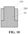
- word line trenches 30 are formed in the substrate 10, a depth of a portion of the word line trench 30 in the AA 40 being smaller than a depth of a portion of the word line trench 30 in the STI structure 20, such that a first protruding structure 310 is formed at a bottom of the portion of the word line trench 30 in the AA 40.
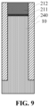
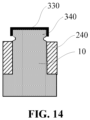
- an etch protection layer 330 is formed on a surface of the first protruding structure 310.
- the STI structure 20 is partially removed to form a second protruding structure 340 based on the first protruding structure 310, an upper-portion sidewall and top of the second protruding structure 340 being covered with the etch protection layer 330, and a lower portion of the second protruding structure 340 being exposed from a removed portion of the STI structure.
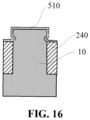
- the lower portion of the second protruding structure 340 is etched to make a width of the lower portion of the second protruding structure 340 smaller than a width of an upper portion of the second protruding structure 340.
- a word line structure 50 is formed in the word line trench 30.
- the second protruding structure 340 is formed at the bottom portion of the word line trench 30 in the AA40 of a semiconductor structure 100 manufactured by the method for manufacturing a semiconductor structure, and the width of the lower portion of the second protruding structure 340 is smaller than the width of the upper portion of the second protruding structure 340, so that a channel width of a gate can be increased on the premise of not increasing a width of an upper portion of the AA 40, resistance between a source and a drain can be reduced, and a current between the source and the drain can be increased.
- the substrate 10 provided in S10 may include any existing semiconductor substrate.
- the substrate 10 may include, but not limited to, a silicon substrate.
- the operation in S10 that the STI structures 20 are formed in the substrate 10 may include the following operations.
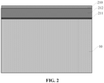
- a first mask layer 210 is formed on an upper surface of the substrate 10.
- the first mask layer 210 is patterned to obtain a first patterned mask layer 220, a plurality of first opening patterns 221 being formed in the first patterned mask layer 220, and the plurality of first opening patterns 221 defining positions of the STI structures 20.
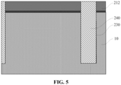
- the substrate 10 is etched based on the first patterned mask layer 220 to form a plurality of shallow trenches 230 in the substrate 10.
- the shallow trenches 230 are filled with an isolation material 240 to form the STI structures 20.
- an oxide layer 211 is formed on the upper surface of the substrate 10
- a nitride layer 212 is formed on an upper surface of the oxide layer 211.
- the first mask layer 210 can be a photoresist layer, and the first mask layer 210 can be formed on the upper surface of the nitride layer 212 using, but not limited to, a spin-on process.
- the oxide layer 211 can be formed using a physical vapor deposition process, a chemical deposition process, a thermal oxidation process, etc.
- the oxide layer 211 can be formed on the surface of the substrate 10 using the thermal oxidation process.
- a thickness of the oxide layer 211 can be set according to actual needs. In the embodiment, the thickness of the oxide layer 211 can be, but not limited to, 3 nm to 15 nm.
- the nitride layer 212 can be formed using the physical vapor deposition process, a Chemical Vapor Deposition (CVD) process, etc.
- the nitride layer 212 can be formed using a Low-Pressure CVD (LPCVD) process.
- the nitride layer 212 may include, but not limited to, silicon oxide.
- a thickness of the nitride layer 212 can be set according to actual needs. In the embodiment, the thickness of the nitride layer 212 can be, but not limited to, 100 nm to 200 nm.
- the first mask layer 210 can be patterned in S120 using a photoetching process to obtain the first patterned mask layer 220.
- the plurality of first opening patterns 221 is formed in the first patterned mask layer 220, and the plurality of first opening patterns 221 defines the positions of the shallow trench 230.
- the oxide layer 211, the nitride layer 212, and the substrate 10 can be simultaneously etched in S130 based on the first patterned mask layer 220, the substrate 10 being etched using, but not limited to, a dry etching process, to form the shallow trench 230 in the substrate 10.
- the shallow trench 230 may include a first shallow trench 231 and a second shallow trench (not shown).
- the first shallow trench 231 can be in the substrate 10 between two adjacent AAs 40 in a length direction of the AA 40 (an extending direction of the AA 40), and the second shallow trench can be in the substrate 10 between two adjacent AAs 40 in a width direction of the AA 40 (perpendicular to the extending direction of the AA 40).
- an operation of removing the first patterned mask layer 220 can be included.
- a distance from the first shallow trench 231 to the upper surface of the substrate 10 can be 250 nm to 350 nm
- a distance from the second shallow trench to the upper surface of the substrate 10 can be 200 nm to 300 nm.
- the operation in S140 that the shallow trench 230 is filled with the isolation material 240 to form the STI structure 20 may include the following operations.
- the isolation material 240 are filled in the shallow trenches 230 and on the upper surface of the etched nitride layer 212.
- the isolation material 240 on the upper surface of the etched nitride layer 212 is removed, and the shallow trenches 230 are filled with the remaining isolation material 240, an upper surface of the remaining isolation material 240 being flush with the upper surface of the patterned nitride layer 212.
- the isolation material 240 can be formed using, but not limited to, a High-Density Plasma-CVD (HDPCVD) process, a Flowable oxide CVD process, or a Spin-on Dielectric (SOD) process.
- the isolation material 240 may include, but not limited to, silicon oxide.
- the isolation material 240 on the upper surface of the etched nitride layer 212 can be removed using, but not limited to, a Chemical Mechanical Polishing (CMP) process.
- CMP Chemical Mechanical Polishing
- the patterned nitride layer 212 can be used as a grinding stopping layer.
- the operation in S20 that the word line trench 30 is formed in the substrate 10 may include the following operations.
- a second mask layer (not shown) is formed on the upper surface of the substrate 10.
- the second mask layer is patterned to obtain a second patterned mask layer 321, a second open pattern 322 being formed in the second patterned mask layer 321, and the second open pattern 322 defining a position of the word line trench 30.
- the substrate 10 is etched based on the second patterned mask layer 321 to form the word line trench 30 in the substrate 10.
- the second mask layer can be patterned in S210 using the photoetching process to obtain the second patterned mask layer 321.
- the second open pattern 322 is formed in the second patterned mask layer 321, and the second open pattern 322 defines the position of the word line trench 30.
- the substrate 10, the oxide layer 211, and the nitride layer 212 can be etched in S220 using, but not limited to, the dry etching process based on the second patterned mask layer 321 to form the word line trench 30 in the substrate 10.
- an operation of removing the second patterned mask layer 321 can be included.
- an intersection angle of an extending direction of the word line trench 30 and the extending direction of the AA 40 can be smaller than 90 degrees.
- the depth of the portion, in the AA 40, of the word line trench 30 is different from the depth of the word line trench 30 in the STI structure 20, and the depth of the portion, in the AA 40, of the word line trench 30 is usually smaller than the depth of the word line trench in the STI structure 20 such that the first protruding structure 310 is formed at the bottom of the portion, in the AA 40, of the word line trench 30.
- wet cleaning and wet etching can be performed on the isolation material 240 in the word line trench 30 using, but not limited to, Hydrogen Fluoride (HF), Diluted HF (DHF) (1:100 to 1:2,000, namely 49% HF: deionized water), Buffered Oxide Etch (BOE), etc., to form the first protruding structure 310.
- a depth of each portion of the word line trench 30 can be set as practically required.
- the depth of the portion, in the AA 40, of the word line trench 30 can be, but not limited to, 90 nm to 160 nm, and the depth of the portion in the STI structure 20 is 100 nm to 180 nm.
- the operation in S30 that the etch protection layer 330 is formed on the surface of the first protruding structure 310 may include the following operation.
- nitrogen is injected to the word line trench 30 at a preset temperature to form the nitride layer on a sidewall and bottom of the portion, in the AA 40, of the word line trench 30 as the etch protection layer 330.
- nitrogen can be injected to the word line trench 30 at a high temperature over 900 °C, partial pressure of the nitrogen being about 0.1 MPa, to form a silicon nitride layer on an exposed sidewall and bottom of the silicon substrate as the etch protection layer 330 to protect the silicon substrate.
- a reaction formula can be represented as: 3Si+2N 2 (g) ⁇ Si 3 N 4 .
- the isolation material 240 can be etched in S40 using, but not limited to, wet cleaning and wet etching processes.
- wet cleaning and wet etching can be performed on the isolation material 230 using, but not limited to, HF, DHF (1:100 to 1:2,000, namely 49% HF: deionized water), BOE, etc., to increase a height difference between the upper surface of the word line trench 30 in the AA 40 and the upper surface in the STI structure 20, namely forming the second protruding structure 340 based on the first protruding structure 310.
- the upper-portion sidewall and top of the second protruding structure 340 are covered with the etch protection layer 330, and the lower portion of the second protruding structure 340 is exposed from a removed portion of the isolation material 240.
- a height of the lower portion of the second protruding structure 340 can be set as practically required.
- the height of the lower portion of the second protruding structure 340 can be, but not limited to, 3 to 20 nm.
- the width of the lower portion of the second protruding structure 340 can be smaller than the width of the upper portion by, but not limited to, 2 to 10 nm.
- an exposed portion of the lower portion of the second protruding structure 340 can be etched in S50 using, but not limited to, wet etching to make the width of the lower portion of the second protruding structure 340 smaller than the width of the upper portion of the second protruding structure 340.
- the substrate 10 is a silicon substrate
- the silicon substrate can be etched using, but not limited to, alkaline liquid such as diluted KOH or NH 4 OH to increase a channel width of the gate, reduce the resistance between the source and the drain, and increase the current between the source and the drain.
- Reaction formulas can be represented as: Si+4OH - ⁇ SiO 2 (OH) 2 -2 +2H + +4e - ; 4e - +4H 2 O ⁇ 4OH - +2H + ; and SiO 2 (OH) 2 -2 +2H + ⁇ Si(OH) 4 ⁇ Si(OH) 3 -O-Si(OH) 3 +H 2 O.
- the operation in S60 that the word line structure 50 is formed in the word line trench 30 may include the following operations.
- a gate dielectric layer 510 is formed on the sidewall of the word line trench 30, the bottom of the word line trench 30, the upper surface of the etched nitride layer 212, and the upper surface of the STI structure 20.
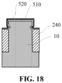
- a first conducting material layer 520 is formed on a surface of the gate dielectric layer 510.
- a second conducting material layer 530 is formed on a surface of the first conducting material layer 520.
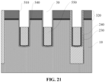
- the first conducting material layer 520 and second conducting material layer 530 on the upper surface of the etched nitride layer 212 and the upper surface of the STI structure 20 are removed, and etching-back is performed to partially remove the first conducting material layer 520 and second conducting material layer 530 in the word line trench 30 to obtain a first conducting layer 540 and a second conducting layer 550, both an upper layer of the first conducting layer 540 and an upper surface of the second conducting layer 550 being lower than a top of the word line trench 30.
- the oxide layer naturally formed on the surface where the gate dielectric layer 510 is to be formed can be removed using, but not limited to, wet etching.
- wet cleaning can be performed using, but not limited to, HF, DHF (1:100 to 1:2,000, namely 49% HF: deionized water), BOE, etc., to remove the oxide layer naturally formed on the sidewall of the word line trench 30, the bottom of the word line trench 30, the upper surface of the etched nitride layer 212, and the upper surface of the STI structure 20.
- the gate dielectric layer 510 in S610 may include a silicon oxide layer, a silicon nitride layer, or a high-k dielectric layer.
- the high-k dielectric layer can be, but not limited to, an alumina layer, a hafnium oxide layer, a hafnium silicon oxide layer, a hafnium alumina layer, a tantalum oxide layer, a zirconia layer, or a stack of the multiple layers.
- a thickness of the gate dielectric layer 510 can be, but not limited to, 3 nm to 7 nm.
- the first conducting material layer 520 can be formed in S620 using, but not limited to, the physical vapor deposition process, the CVD process, etc.
- the first conducting material layer 520 may include, but not limited to, a titanium nitride layer.
- a thickness of the first conducting material layer 520 can be, but not limited to, 2 nm to 5 nm.
- the second conducting material layer 530 can be formed in S630 using an electroplating process, etc.
- the second conducting material layer 530 may include, but not limited to, a tungsten layer.
- the first conducting material layer 520 and second conducting material layer 530 on the upper surface of the patterned nitride layer 212 can be removed in S640 using a CMP process. After etching-back, both the upper surface of the first conducting layer 540 and the upper surface of the second conducting layer 550 are lower than the top of the word line trench 30, and the upper surface of the second conducting layer 550 is higher than the upper surface of the first conducting layer 540.
- the operation that the etch protection layer 330 is formed on the surface of the first protruding structure 310 may include the following operation: an epitaxial layer 331 is formed on the sidewall and bottom of the portion, in the AA 40, of the word line trench 30 using an epitaxial growth method, a material of the epitaxial layer 331 being the same as a material of the substrate 10.
- the epitaxial layer 331 can be grown on the sidewall and bottom of the word line trench 30 using, but not limited to, a Vapor Phase Epitaxy (VPE) process, a Molecular Beam Epitaxy (MBE) process, and a Liquid Phase Epitaxy (LPE) process.
- VPE Vapor Phase Epitaxy
- MBE Molecular Beam Epitaxy
- LPE Liquid Phase Epitaxy
- the substrate 10 is a silicon substrate
- epitaxial silicon can be grown on the sidewall and bottom of the word line trench as the epitaxial layer 331 using the abovementioned processes to ensure that the material of the epitaxial layer 331 is the same as the material of the substrate 10.
- the operation that the word line structure 50 is formed in the word line trench 30 may include the following operations.
- the gate dielectric layer 510 is formed on the sidewall and bottom of the word line trench 30.
- the first conducting material layer 520 is formed on the surface of the gate dielectric layer 510.
- the second conducting material layer 530 is formed on the surface of the first conducting material layer 520.
- the first conducting material layer 520 and the second conducting material layer 530 are etched back to obtain the first conducting layer 540 and the second conducting layer 550, both the upper surface of the first conducting layer 540 and the upper surface of the second conducting layer 550 being lower than the top of the word line trench 30.
- the oxide layer naturally formed on the surface where the gate dielectric layer 510 is to be formed can be removed using, but not limited to, wet etching.
- wet cleaning can be performed using, but not limited to, HF, DHF (1:100 to 1:2,000, namely 49% HF: deionized water), BOE, etc., to remove the oxide layer naturally formed on the sidewall of the word line trench 30, the bottom of the word line trench 30, the upper surface of the etched nitride layer 212, and the upper surface of the STI structure 20.
- the substrate can be oxidized in S650 using an In Situ Steam Generation (ISSG) process to form the gate dielectric layer 510.
- the gate dielectric layer 510 can be a silicon oxide layer.
- the thickness of the gate dielectric layer 510 can be set as practically required. In the embodiment, the thickness of the gate dielectric layer 510 can be, but not limited to, 3 nm to 7 nm.
- S660 to S680 can be the same as S620 to S640.
- the etch protection layer 330 may include an oxide layer or a nitride layer. In the embodiment, before the gate dielectric layer 510 is formed, an operation of removing the etch protection layer 330 may further be included.
- the oxide layer and the nitride layer are formed on the sidewall and bottom of the word line trench 30 as the etch protection layer 330 in S330, before the word line structure 50 is formed in the word line trench 30 in S60, namely before the gate dielectric layer 510 is formed, the operation of removing the etch protection layer 330 is further included.
- the substrate 10 is a silicon substrate, and a silicon nitride is used as the etch protection layer, the silicon nitride can be removed using, but not limited to, wet etching.
- the silicon nitride can be etched using a hot solution of H 3 PO 4 at a temperature ranging from 110 °C to 165 °C, and the silicon nitride can be removed by accurately controlling action time of the solution. It is to be noted that, in such case, a surface of the silicon nitride used as the nitride layer 212 is also etched slightly.
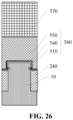
- a filler insulating layer 570 is formed in the word line trench 30 and the upper surface of the etched nitride layer 212.
- the filler insulating layer 570 can be formed using, but not limited to, the LPCVD process.
- the filler insulating layer 570 may include, but not limited to, a silicon nitride layer.
- a drain (not shown) and a source (not shown) are formed in the AA 40, the drain being located between word lines 50 across the same AA 40, and the source being on the side of the word line 560 distal from the drain.
- the etched nitride layer 212, gate dielectric layer 510, first conducting material layer 520, and second conducting material layer 530 on the upper surface of the substrate 10 can be removed at first.
- the application also provides a semiconductor structure 100.
- the semiconductor structure 100 includes a substrate 10, STI structures 20, word line trenches 30 formed in the substrate 10, and word lines 560.
- the STI structures 20 isolate a plurality of spaced AAs 40 in the substrate 10.
- the word line trench 30 is in the substrate 10, a protruding structure 350 is formed at a bottom of a portion, in the AA 40, of the word line trench 30, and a width of a lower portion of the protruding portion 350 is smaller than a width of an upper portion of the protruding portion 350.
- the word line 560 is in the word line trench 30.
- the protruding structure 350 is formed at the bottom portion of the word line trench 30 in the AA 40 of the semiconductor structure 100, and the width of the lower portion of the protruding structure 350 is smaller than the width of the upper portion of the protruding structure 350, so that a channel width of a gate can be increased on the premise of not increasing a width of an upper portion of the AA 40, resistance between a source and a drain can be reduced, and a current between the source and the drain can be increased.
- the substrate 10 may include any existing semiconductor substrate.
- the substrate 10 may include, but not limited to, a silicon substrate.
- shallow trenches 230 are formed in the substrate 10, and the shallow trenches 230 can be filled with an isolation material 240 to form the STI structures 20.
- the shallow trench 230 may include a first shallow trench 231 and a second shallow trench.
- the first shallow trench 231 can be in the substrate 10 between two adjacent AAs 40 in a length direction of the AA 40 (an extending direction of the AA 40), and the second shallow trench can be in the substrate 10 between two adjacent AAs 40 in a width direction of the AA 40 (perpendicular to the extending direction of the AA 40).
- a distance from the first shallow trench 231 to an upper surface of the substrate 10 can be 250 nm to 350 nm
- a distance from the second shallow trench to the upper surface of the substrate 10 can be 200 nm to 300 nm.
- the word line trench 30 is formed in the substrate 10, and the word line 560 is in the word line trench 30, so a word line structure 50 is formed.
- an intersection angle of an extending direction of the word line trench 30 and the extending direction of the AA 40 can be smaller than 90 degrees.
- a distance between the bottom portion of the word line trench 30 in the AA 40 and the upper surface of the substrate 10 and a distance between a bottom portion of the word line trench 30 in the STI structure 20 and the upper surface of the substrate 10 can be set according to actual needs.
- the distance between the bottom portion of the word line trench 30 in the AA 40 and the upper surface of the substrate 10 is, not limited to, 90 to 160 nm
- the distance between the bottom of the portion, in the STI structure 20, of the word line trench 30 and the upper surface of the substrate 10 is, but not limited to, 100 nm to 180 nm.
- a height of the lower portion of the protruding structure 350 can be set as practically required.
- the height of the lower portion of the protruding structure 350 is, but not limited to, 3 to 20 nm.
- the width of the lower portion of the protruding structure 350 can be smaller than the width of the upper portion by, but not limited to, 2 to 10 nm.
- the word line 560 includes a gate dielectric layer 510, a first conducting layer 540, and a second conducting layer 550.
- the gate dielectric layer 510 can be on a sidewall and bottom of the word line trench 30, and may include a silicon oxide layer, a silicon nitride layer, or a high-k dielectric layer.
- a thickness of the gate dielectric layer 510 can be set as practically required. In the embodiment, the thickness of the gate dielectric layer 510 can be, but not limited to, 3 nm to 7 nm.
- the first conducting layer 540 is in the word line trench 30 and on a surface of the gate dielectric layer 510, and an upper surface of the first conducting layer 540 is lower than a top of the word line trench 30.
- the first conducting layer 540 may include, but not limited to, a titanium nitride layer.
- a thickness of the first conducting layer 540 can be set as practically required. In the embodiment, the thickness of the first conducting layer 540 can be, but not limited to, 2 nm to 5 nm.
- the second conducting layer 550 is in the word line trench 30 and on a surface of the first conducting layer 540, and an upper surface of the second conducting layer 550 is lower than the top of the word line trench 30.
- a height of the upper surface of the second conducting layer 550 can be equal to a height of the upper surface of the first conducting layer 540.
- the second conducting layer 550 can be, but not limited to, a tungsten layer.
- the semiconductor structure further includes a filler insulating layer 570.
- the filler insulating layer 570 is on the word line 560, and the filler insulating layer 570 fills the word line trench 30, and covers an upper layer of a patterned nitride layer 212.
- the filler insulating layer 570 may include, but not limited to, a silicon nitride layer.
- the semiconductor structure 100 further includes drains (not shown), the drain being in the AA 40 and between two word lines 560 across the same AA 40, and sources (not shown), located in the AAs 40 and on the sides of the word lines 560 distal from the drains.
Landscapes
- Engineering & Computer Science (AREA)
- Manufacturing & Machinery (AREA)
- Semiconductor Memories (AREA)
Claims (15)
- Procédé de fabrication d'une structure semi-conductrice, le procédé comprenant ;de fournir (S10) un substrat (10), et de former des structures (20) d'isolation par tranchées peu profondes, STI, dans le substrat, les structures de STI isolant une pluralité de zones actives, AA, (40) espacées dans le substrat ;de former (S20) des tranchées de ligne de mots (30) dans le substrat (10), une profondeur d'une partie de la tranchée de ligne de mots (30) dans l'AA (40) étant plus petite qu'une profondeur d'une partie dans la structure de STI (20) de telle manière qu'une première structure saillante (310) est formée en un fond de la partie de la tranchée de ligne de mots (30) dans l'AA (40) ;de former (S30) une couche de protection anti-attaque (330) sur une surface de la première structure saillante (310) ;d'enlever partiellement (S40) la structure de STI (20) pour former une seconde structure saillante (340) basée sur la première structure saillante (310), une paroi latérale de partie supérieure et le haut de la seconde structure saillante (340) étant couverts avec la couche de protection anti-attaque (330), et une partie inférieure de la seconde structure saillante (340) étant exposée par une partie enlevée de la structure de STI (20) ;d'attaquer (S50) la partie inférieure de la seconde structure saillante (340) pour rendre une largeur de la partie inférieure de la seconde structure saillante (340) plus petite qu'une largeur d'une partie supérieure de la seconde structure saillante (340) ; etde former (S60) une structure de ligne de mots dans la tranchée de ligne de mots (30).
- Procédé selon la revendication 1, dans lequel former (S30) la couche de protection anti-attaque (330) sur la surface de la première structure saillante (310) comprend :
d'injecter de l'azote dans la tranchée de ligne de mots (30) a une température préétablie pour former une couche de nitrure comme la couche de protection anti-attaque (330) sur une paroi latérale et le fond de la partie de la tranchée de ligne de mots (30) dans l'AA (40). - Procédé selon la revendication 1, dans lequel ladite formation des structures de STI (20) dans le substrat (10) comprend :
de former une première couche de masquage (210) sur une surface supérieure du substrat :de donner un motif à la première couche de masquage (210) pour obtenir une première couche de masquage à motif (220), une pluralité de premiers motifs d'ouverture (221) étant formés dans la première couche de masquage à motif (220), et la pluralité de premiers motifs d'ouverture (221) définissant des positions des structures de STI (20) ;d'attaquer le substrat (10) en se basant sur la première couche de masquage à motif (220) pour former une pluralité de tranchées peu profondes (230) dans le substrat (10) ; etde remplir les tranchées peu profondes (230) avec un matériau isolant (240) pour former les structures de STI (20). - Procédé selon la revendication 3, dans lequel avant ladite formation de ladite première couche de masquage (210) sur la surface supérieure du substrat, le procédé comprend en outre de former une couche d'oxyde (211) sur la surface supérieure du substrat (10), et de former ensuite une couche de nitrure (212) sur une surface supérieure de la couche d'oxyde (211).
- Procédé selon la revendication 4, dans lequel ledit remplissage des tranchées peu profondes (230) avec le matériau isolant (240) pour former les structures de STI (20) comprend :de remplir le matériau isolant (240) dans les tranchées peu profondes (230) et sur une surface supérieure de la couche de nitrure (212) attaquée ; etd'enlever le matériau isolant (240) sur la surface supérieure de la couche de nitrure (212) attaquée, et remplir les tranchées peu profondes (230) avec le matériau isolant (240) restant, une surface supérieure du matériau isolant (240) restant étant à niveau avec la surface supérieure de la couche de nitrure (212).
- Procédé selon la revendication 5, dans lequel ladite formation de la structure de ligne de mots dans la tranchée de ligne de mots (30) comprend :de former une couche diélectrique de grille (510) sur la paroi latérale de la tranchée de ligne de mots (30), le fond de la tranchée de ligne de mots (30), la surface supérieure de la couche de nitrure (212), et une surface supérieure de la structure de STI (20) ;de former une première couche de matériau conducteur (520) sur une surface de la couche diélectrique de grille (510) ;de former une seconde couche de matériau conducteur (530) sur une surface de la première couche de matériau conducteur (520) ; etd'enlever la première couche de matériau conducteur (520) et la seconde couche de matériau conducteur (530) sur la surface supérieure de la couche de nitrure (212) attaquée et la surface supérieure de la structure de STI (20), et de réaliser une attaque pour enlever partiellement la première couche de matériau conducteur (520) et la seconde couche de matériau conducteur (530) dans la tranchée de ligne de mots (30) pour obtenir une première couche conductrice (540) et une seconde couche conductrice (550), à la fois une couche supérieure de la première couche conductrice (540) et une surface supérieure de la seconde couche conductrice (550) étant plus basses qu'un haut de la tranchée de ligne de mots (30).
- Procédé selon la revendication 1, dans lequel ladite formation de ladite tranchée de ligne de mots (30) dans le substrat (10) comprend :de former une seconde couche de masquage sur la surface supérieure du substrat (10) ;de former un motif sur la seconde couche de masquage pour obtenir une seconde couche de masquage à motif (321), la seconde couche de masquage à motif (321) ayant un second motif ouvert (322), et le second motif ouvert (322) définissant une position de la tranchée de ligne de mots (30) ; etd'attaquer le substrat (10) en se basant sur la seconde couche de masquage à motif (321) pour former la tranchée de ligne de mots (30) dans le substrat (10).
- Procédé selon la revendication 1, dans lequel ladite formation de la structure de ligne de mots dans la tranchée de ligne de mots (30) comprend :de former la couche diélectrique de grille (510) sur la paroi latérale et le fond de la tranchée de ligne de mots (30) ;de former la première couche de matériau conducteur (520) sur la surface de la couche diélectrique de grille (510) ;de former la seconde couche de matériau conducteur (530) sur la surface de la première couche de matériau conducteur (520) ; etd'attaquer la première couche de matériau conducteur (520) et la seconde couche de matériau conducteur (530) pour obtenir la première couche conductrice (540) et la seconde couche conductrice (550), à la fois la surface supérieure de la première couche conductrice (540) et la surface supérieure de la seconde couche conductrice (550) étant plus basses que le haut de la tranchée de ligne de mots (30).
- Procédé selon la revendication 8, dans lequel avant la formation de la couche diélectrique de grille (510), le procédé comprend en outre : d'enlever la couche de protection anti-attaque (330) ; ou
après ladite attaque de la première couche de matériau conducteur (520) et de la seconde couche de matériau conducteur (530) pour obtenir la première couche conductrice (540) et la seconde couche conductrice (550), le procédé comprend en outre : de former une couche isolante de remplissage (570) dans la tranchée de ligne de mots (30) et sur la surface supérieure de la couche de nitrure (212). - Procédé selon la revendication 8, dans lequel la couche diélectrique de grille (510) comprend une couche d'oxyde de silicium, une couche de nitrure de silicium, ou une couche diélectrique à haut-k, dans lequel la couche diélectrique à haut-k est une couche d'alumine, une couche d'oxyde d'hafnium, une couche d'oxyde de silicium hafnium, une couche d'alumine hafnium, une couche d'oxyde de tantale, une couche de zircone, ou un empilement des multiples couches.
- Procédé selon la revendication 8, comprenant en outre :de former un drain et une source dans l'AA (40), le drain étant situé entre des lignes de mots (50) à travers la même AA (40), et la source étant située sur le côté de la ligne de mots de grille (560) distale du drain ; etavant de former le drain et la source, le procédé comprenant en outre d'enlever la couche de nitrure (212) attaquée sur la surface du substrat (10), la couche diélectrique de grille (510), la première couche de matériau conducteur (520), et la seconde couche de matériau conducteur (530).
- Procédé selon la revendication 1, dans lequel ladite formation de la couche de protection anti-attaque (330) sur la surface de la première structure saillante (310) comprend : de former une couche épitaxiale (331) sur la paroi latérale et le fond de la partie de la tranchée de ligne de mots dans l'AA (40) par une croissance épitaxiale, un matériau de la couche épitaxiale (331) étant le même qu'un matériau du substrat (10).
- Structure semi-conductrice, comprenant :un substrat (10) ;des structures (20) d'isolation par tranchées peu profondes, STI, isolant une pluralité de zones actives, AA, (40) espacées dans le substrat (10) ;des tranchées de lignes de mots (30), situées dans le substrat (10), etdes lignes de mots (50), situées dans les tranchées de ligne de mots (30), caractérisée en ce que la structure semi-conductrice comprend en outre :
une structure saillante (310) étant formée en une partie de fond de la tranchée de ligne de mots dans l'AA (40), et une largeur d'une partie inférieure de la structure saillante (310) étant plus petite qu'une largeur d'une partie supérieure de la structure saillante (310), dans laquelle une direction de la largeur de la partie inférieure de la structure saillante (310) et une direction de la largeur de la partie supérieure de la structure saillante (310) sont parallèles à une direction d'extension de la tranchée de ligne de mots. - Structure semi-conductrice selon la revendication 13, dans laquelle une hauteur de la partie inférieure de la structure saillante (310) est de 3 à 20 nm, et la largeur de la partie inférieure de la structure saillante (310) est inférieure à la largeur de la partie supérieure de 2 à 10 nm.
- Structure semi-conductrice selon la revendication 14, dans laquelle une distance entre la partie inférieure de la tranchée de ligne de mots dans l'AA (40) et une surface supérieure du substrat (10) est de 90 à 160 nm, et une distance entre une partie inférieure de la tranchée de ligne de mots dans la structure de STI (20) et la surface supérieure du substrat (10) est de 100 nm à 180 nm.
Applications Claiming Priority (2)
| Application Number | Priority Date | Filing Date | Title |
|---|---|---|---|
| CN202010441445.9A CN113707600B (zh) | 2020-05-22 | 2020-05-22 | 半导体结构及其制备方法 |
| PCT/CN2021/094286 WO2021233276A1 (fr) | 2020-05-22 | 2021-05-18 | Structure semi-conductrice et son procédé de fabrication |
Publications (3)
| Publication Number | Publication Date |
|---|---|
| EP3958314A1 EP3958314A1 (fr) | 2022-02-23 |
| EP3958314A4 EP3958314A4 (fr) | 2022-08-24 |
| EP3958314B1 true EP3958314B1 (fr) | 2024-01-31 |
Family
ID=78705395
Family Applications (1)
| Application Number | Title | Priority Date | Filing Date |
|---|---|---|---|
| EP21800975.1A Active EP3958314B1 (fr) | 2020-05-22 | 2021-05-18 | Structure semi-conductrice et son procédé de fabrication |
Country Status (2)
| Country | Link |
|---|---|
| US (1) | US12144166B2 (fr) |
| EP (1) | EP3958314B1 (fr) |
Families Citing this family (3)
| Publication number | Priority date | Publication date | Assignee | Title |
|---|---|---|---|---|
| CN114078853B (zh) * | 2020-08-18 | 2023-02-24 | 长鑫存储技术有限公司 | 存储器及其制作方法 |
| US11871564B2 (en) * | 2021-03-31 | 2024-01-09 | Changxin Memory Technologies, Inc. | Semiconductor structure and manufacturing method thereof |
| US20230029202A1 (en) * | 2021-07-21 | 2023-01-26 | Changxin Memory Technologies, Inc. | Contact structure forming method, contact structure, and semiconductor device |
Family Cites Families (15)
| Publication number | Priority date | Publication date | Assignee | Title |
|---|---|---|---|---|
| DE10131276B4 (de) | 2001-06-28 | 2007-08-02 | Infineon Technologies Ag | Feldeffekttransistor und Verfahren zu seiner Herstellung |
| US7442976B2 (en) | 2004-09-01 | 2008-10-28 | Micron Technology, Inc. | DRAM cells with vertical transistors |
| KR100724575B1 (ko) * | 2006-06-28 | 2007-06-04 | 삼성전자주식회사 | 매립 게이트전극을 갖는 반도체소자 및 그 형성방법 |
| JP2008118007A (ja) | 2006-11-07 | 2008-05-22 | Toshiba Corp | 不揮発性半導体記憶装置およびその製造方法 |
| KR101073073B1 (ko) * | 2008-10-17 | 2011-10-12 | 주식회사 하이닉스반도체 | 수직게이트를 구비한 반도체장치 및 그 제조 방법 |
| JP2010161173A (ja) * | 2009-01-07 | 2010-07-22 | Renesas Electronics Corp | 半導体記憶装置 |
| US8569831B2 (en) * | 2011-05-27 | 2013-10-29 | Micron Technology, Inc. | Integrated circuit arrays and semiconductor constructions |
| US8603891B2 (en) | 2012-01-20 | 2013-12-10 | Micron Technology, Inc. | Methods for forming vertical memory devices and apparatuses |
| US9947666B2 (en) * | 2012-01-20 | 2018-04-17 | Micron Technology, Inc. | Semiconductor device structures including buried digit lines and related methods |
| US8710570B2 (en) * | 2012-07-24 | 2014-04-29 | SK Hynix Inc. | Semiconductor device having vertical channel |
| KR102110464B1 (ko) * | 2013-11-25 | 2020-05-13 | 에스케이하이닉스 주식회사 | 반도체 소자 및 그 제조 방법 |
| US9768177B2 (en) * | 2015-08-04 | 2017-09-19 | Micron Technology, Inc. | Method of forming conductive material of a buried transistor gate line and method of forming a buried transistor gate line |
| CN107342327A (zh) | 2017-08-10 | 2017-11-10 | 睿力集成电路有限公司 | 一种半导体存储器的晶体管结构及制作方法 |
| CN109979939B (zh) | 2017-12-27 | 2021-09-28 | 长鑫存储技术有限公司 | 半导体存储器件结构及其制作方法 |
| CN210575894U (zh) | 2019-11-29 | 2020-05-19 | 长鑫存储技术有限公司 | 浅沟槽隔离结构及半导体结构 |
-
2021
- 2021-05-18 EP EP21800975.1A patent/EP3958314B1/fr active Active
- 2021-08-14 US US17/445,085 patent/US12144166B2/en active Active
Also Published As
| Publication number | Publication date |
|---|---|
| EP3958314A4 (fr) | 2022-08-24 |
| EP3958314A1 (fr) | 2022-02-23 |
| US12144166B2 (en) | 2024-11-12 |
| US20210375879A1 (en) | 2021-12-02 |
Similar Documents
| Publication | Publication Date | Title |
|---|---|---|
| US6331469B1 (en) | Trench isolation structure, semiconductor device having the same, and trench isolation method | |
| KR100787685B1 (ko) | 트렌치 캐패시터용 매립 스트랩 제조 방법 | |
| US7682885B2 (en) | Method for fabricating vertical channel transistor in a semiconductor device | |
| EP3958314A1 (fr) | Structure semi-conductrice et son procédé de fabrication | |
| KR100360739B1 (ko) | 트렌치 캐패시터 및 반도체 트랜지스터 구조체와 그 형성 방법 | |
| US20120104539A1 (en) | Trenches with reduced silicon loss | |
| US20140175597A1 (en) | Trench with reduced silicon loss | |
| KR20200049614A (ko) | 채널들로서의 스태킹된 반도체층들을 갖는 트랜지스터들 | |
| JP3802530B2 (ja) | 半導体装置及びその製造方法 | |
| CN117637814A (zh) | 一种半导体器件及其制作方法 | |
| CN113871393A (zh) | 三维存储器的制作方法 | |
| EP2893558B1 (fr) | Procédé de production d'un dispositif microélectronique dans un substrat semi-conducteur monocristallin comportant des tranchées d'isolation partiellement formées sous une zone active | |
| CN113707600B (zh) | 半导体结构及其制备方法 | |
| US7018927B2 (en) | Method for forming isolation film for semiconductor devices | |
| KR20050043424A (ko) | 트랜지스터의 리세스 채널 형성 방법 | |
| KR100733685B1 (ko) | 반도체 소자의 트렌치 형성 방법 | |
| KR20040059445A (ko) | 반도체 소자의 트렌치형 소자분리막 형성방법 | |
| CN114023689B (zh) | Fdsoi的硅外延方法 | |
| KR100646965B1 (ko) | 플래시 메모리 소자의 제조 방법 | |
| KR100446285B1 (ko) | 라운드 모양의 상부 코너를 가지는 트렌치 소자분리영역 형성방법 | |
| US20050158963A1 (en) | Method of forming planarized shallow trench isolation | |
| KR100870303B1 (ko) | 플래쉬 메모리 소자의 제조 방법 | |
| KR100608375B1 (ko) | 반도체 소자의 게이트 형성방법 | |
| KR20090063656A (ko) | 소자 분리막 형성 방법 | |
| KR20030048549A (ko) | 플래쉬 메모리 셀의 제조방법 |
Legal Events
| Date | Code | Title | Description |
|---|---|---|---|
| STAA | Information on the status of an ep patent application or granted ep patent |
Free format text: STATUS: UNKNOWN |
|
| STAA | Information on the status of an ep patent application or granted ep patent |
Free format text: STATUS: THE INTERNATIONAL PUBLICATION HAS BEEN MADE |
|
| PUAI | Public reference made under article 153(3) epc to a published international application that has entered the european phase |
Free format text: ORIGINAL CODE: 0009012 |
|
| STAA | Information on the status of an ep patent application or granted ep patent |
Free format text: STATUS: REQUEST FOR EXAMINATION WAS MADE |
|
| 17P | Request for examination filed |
Effective date: 20211115 |
|
| AK | Designated contracting states |
Kind code of ref document: A1 Designated state(s): AL AT BE BG CH CY CZ DE DK EE ES FI FR GB GR HR HU IE IS IT LI LT LU LV MC MK MT NL NO PL PT RO RS SE SI SK SM TR |
|
| A4 | Supplementary search report drawn up and despatched |
Effective date: 20220722 |
|
| RIC1 | Information provided on ipc code assigned before grant |
Ipc: H01L 27/108 20060101AFI20220718BHEP |
|
| DAV | Request for validation of the european patent (deleted) | ||
| DAX | Request for extension of the european patent (deleted) | ||
| STAA | Information on the status of an ep patent application or granted ep patent |
Free format text: STATUS: EXAMINATION IS IN PROGRESS |
|
| 17Q | First examination report despatched |
Effective date: 20230320 |
|
| REG | Reference to a national code |
Ref country code: DE Free format text: PREVIOUS MAIN CLASS: H01L0027108000 Ref country code: DE Ref legal event code: R079 Ref document number: 602021009095 Country of ref document: DE Free format text: PREVIOUS MAIN CLASS: H01L0027108000 Ipc: H10B0012000000 |
|
| GRAP | Despatch of communication of intention to grant a patent |
Free format text: ORIGINAL CODE: EPIDOSNIGR1 |
|
| STAA | Information on the status of an ep patent application or granted ep patent |
Free format text: STATUS: GRANT OF PATENT IS INTENDED |
|
| RIC1 | Information provided on ipc code assigned before grant |
Ipc: H01L 21/762 20060101ALI20230726BHEP Ipc: H10B 12/00 20230101AFI20230726BHEP |
|
| INTG | Intention to grant announced |
Effective date: 20230828 |
|
| RIN1 | Information on inventor provided before grant (corrected) |
Inventor name: HSU, CHENG-HUNG |
|
| P01 | Opt-out of the competence of the unified patent court (upc) registered |
Effective date: 20230916 |
|
| GRAS | Grant fee paid |
Free format text: ORIGINAL CODE: EPIDOSNIGR3 |
|
| GRAA | (expected) grant |
Free format text: ORIGINAL CODE: 0009210 |
|
| STAA | Information on the status of an ep patent application or granted ep patent |
Free format text: STATUS: THE PATENT HAS BEEN GRANTED |
|
| AK | Designated contracting states |
Kind code of ref document: B1 Designated state(s): AL AT BE BG CH CY CZ DE DK EE ES FI FR GB GR HR HU IE IS IT LI LT LU LV MC MK MT NL NO PL PT RO RS SE SI SK SM TR |
|
| REG | Reference to a national code |
Ref country code: GB Ref legal event code: FG4D Ref country code: CH Ref legal event code: EP |
|
| REG | Reference to a national code |
Ref country code: DE Ref legal event code: R096 Ref document number: 602021009095 Country of ref document: DE |
|
| REG | Reference to a national code |
Ref country code: IE Ref legal event code: FG4D |
|
| REG | Reference to a national code |
Ref country code: LT Ref legal event code: MG9D |
|
| REG | Reference to a national code |
Ref country code: NL Ref legal event code: MP Effective date: 20240131 |
|
| PG25 | Lapsed in a contracting state [announced via postgrant information from national office to epo] |
Ref country code: IS Free format text: LAPSE BECAUSE OF FAILURE TO SUBMIT A TRANSLATION OF THE DESCRIPTION OR TO PAY THE FEE WITHIN THE PRESCRIBED TIME-LIMIT Effective date: 20240531 |
|
| PG25 | Lapsed in a contracting state [announced via postgrant information from national office to epo] |
Ref country code: LT Free format text: LAPSE BECAUSE OF FAILURE TO SUBMIT A TRANSLATION OF THE DESCRIPTION OR TO PAY THE FEE WITHIN THE PRESCRIBED TIME-LIMIT Effective date: 20240131 |
|
| PG25 | Lapsed in a contracting state [announced via postgrant information from national office to epo] |
Ref country code: GR Free format text: LAPSE BECAUSE OF FAILURE TO SUBMIT A TRANSLATION OF THE DESCRIPTION OR TO PAY THE FEE WITHIN THE PRESCRIBED TIME-LIMIT Effective date: 20240501 |
|
| REG | Reference to a national code |
Ref country code: AT Ref legal event code: MK05 Ref document number: 1654712 Country of ref document: AT Kind code of ref document: T Effective date: 20240131 |
|
| PG25 | Lapsed in a contracting state [announced via postgrant information from national office to epo] |
Ref country code: HR Free format text: LAPSE BECAUSE OF FAILURE TO SUBMIT A TRANSLATION OF THE DESCRIPTION OR TO PAY THE FEE WITHIN THE PRESCRIBED TIME-LIMIT Effective date: 20240131 Ref country code: NL Free format text: LAPSE BECAUSE OF FAILURE TO SUBMIT A TRANSLATION OF THE DESCRIPTION OR TO PAY THE FEE WITHIN THE PRESCRIBED TIME-LIMIT Effective date: 20240131 Ref country code: RS Free format text: LAPSE BECAUSE OF FAILURE TO SUBMIT A TRANSLATION OF THE DESCRIPTION OR TO PAY THE FEE WITHIN THE PRESCRIBED TIME-LIMIT Effective date: 20240430 |
|
| PG25 | Lapsed in a contracting state [announced via postgrant information from national office to epo] |
Ref country code: ES Free format text: LAPSE BECAUSE OF FAILURE TO SUBMIT A TRANSLATION OF THE DESCRIPTION OR TO PAY THE FEE WITHIN THE PRESCRIBED TIME-LIMIT Effective date: 20240131 |
|
| PG25 | Lapsed in a contracting state [announced via postgrant information from national office to epo] |
Ref country code: AT Free format text: LAPSE BECAUSE OF FAILURE TO SUBMIT A TRANSLATION OF THE DESCRIPTION OR TO PAY THE FEE WITHIN THE PRESCRIBED TIME-LIMIT Effective date: 20240131 |
|
| PG25 | Lapsed in a contracting state [announced via postgrant information from national office to epo] |
Ref country code: RS Free format text: LAPSE BECAUSE OF FAILURE TO SUBMIT A TRANSLATION OF THE DESCRIPTION OR TO PAY THE FEE WITHIN THE PRESCRIBED TIME-LIMIT Effective date: 20240430 Ref country code: NO Free format text: LAPSE BECAUSE OF FAILURE TO SUBMIT A TRANSLATION OF THE DESCRIPTION OR TO PAY THE FEE WITHIN THE PRESCRIBED TIME-LIMIT Effective date: 20240430 Ref country code: NL Free format text: LAPSE BECAUSE OF FAILURE TO SUBMIT A TRANSLATION OF THE DESCRIPTION OR TO PAY THE FEE WITHIN THE PRESCRIBED TIME-LIMIT Effective date: 20240131 Ref country code: LT Free format text: LAPSE BECAUSE OF FAILURE TO SUBMIT A TRANSLATION OF THE DESCRIPTION OR TO PAY THE FEE WITHIN THE PRESCRIBED TIME-LIMIT Effective date: 20240131 Ref country code: IS Free format text: LAPSE BECAUSE OF FAILURE TO SUBMIT A TRANSLATION OF THE DESCRIPTION OR TO PAY THE FEE WITHIN THE PRESCRIBED TIME-LIMIT Effective date: 20240531 Ref country code: HR Free format text: LAPSE BECAUSE OF FAILURE TO SUBMIT A TRANSLATION OF THE DESCRIPTION OR TO PAY THE FEE WITHIN THE PRESCRIBED TIME-LIMIT Effective date: 20240131 Ref country code: GR Free format text: LAPSE BECAUSE OF FAILURE TO SUBMIT A TRANSLATION OF THE DESCRIPTION OR TO PAY THE FEE WITHIN THE PRESCRIBED TIME-LIMIT Effective date: 20240501 Ref country code: FI Free format text: LAPSE BECAUSE OF FAILURE TO SUBMIT A TRANSLATION OF THE DESCRIPTION OR TO PAY THE FEE WITHIN THE PRESCRIBED TIME-LIMIT Effective date: 20240131 Ref country code: ES Free format text: LAPSE BECAUSE OF FAILURE TO SUBMIT A TRANSLATION OF THE DESCRIPTION OR TO PAY THE FEE WITHIN THE PRESCRIBED TIME-LIMIT Effective date: 20240131 Ref country code: BG Free format text: LAPSE BECAUSE OF FAILURE TO SUBMIT A TRANSLATION OF THE DESCRIPTION OR TO PAY THE FEE WITHIN THE PRESCRIBED TIME-LIMIT Effective date: 20240131 Ref country code: AT Free format text: LAPSE BECAUSE OF FAILURE TO SUBMIT A TRANSLATION OF THE DESCRIPTION OR TO PAY THE FEE WITHIN THE PRESCRIBED TIME-LIMIT Effective date: 20240131 |
|
| PG25 | Lapsed in a contracting state [announced via postgrant information from national office to epo] |
Ref country code: PL Free format text: LAPSE BECAUSE OF FAILURE TO SUBMIT A TRANSLATION OF THE DESCRIPTION OR TO PAY THE FEE WITHIN THE PRESCRIBED TIME-LIMIT Effective date: 20240131 Ref country code: PT Free format text: LAPSE BECAUSE OF FAILURE TO SUBMIT A TRANSLATION OF THE DESCRIPTION OR TO PAY THE FEE WITHIN THE PRESCRIBED TIME-LIMIT Effective date: 20240531 |
|
| PG25 | Lapsed in a contracting state [announced via postgrant information from national office to epo] |
Ref country code: SE Free format text: LAPSE BECAUSE OF FAILURE TO SUBMIT A TRANSLATION OF THE DESCRIPTION OR TO PAY THE FEE WITHIN THE PRESCRIBED TIME-LIMIT Effective date: 20240131 Ref country code: PT Free format text: LAPSE BECAUSE OF FAILURE TO SUBMIT A TRANSLATION OF THE DESCRIPTION OR TO PAY THE FEE WITHIN THE PRESCRIBED TIME-LIMIT Effective date: 20240531 Ref country code: PL Free format text: LAPSE BECAUSE OF FAILURE TO SUBMIT A TRANSLATION OF THE DESCRIPTION OR TO PAY THE FEE WITHIN THE PRESCRIBED TIME-LIMIT Effective date: 20240131 Ref country code: LV Free format text: LAPSE BECAUSE OF FAILURE TO SUBMIT A TRANSLATION OF THE DESCRIPTION OR TO PAY THE FEE WITHIN THE PRESCRIBED TIME-LIMIT Effective date: 20240131 |
|
| PG25 | Lapsed in a contracting state [announced via postgrant information from national office to epo] |
Ref country code: DK Free format text: LAPSE BECAUSE OF FAILURE TO SUBMIT A TRANSLATION OF THE DESCRIPTION OR TO PAY THE FEE WITHIN THE PRESCRIBED TIME-LIMIT Effective date: 20240131 |
|
| PG25 | Lapsed in a contracting state [announced via postgrant information from national office to epo] |
Ref country code: SM Free format text: LAPSE BECAUSE OF FAILURE TO SUBMIT A TRANSLATION OF THE DESCRIPTION OR TO PAY THE FEE WITHIN THE PRESCRIBED TIME-LIMIT Effective date: 20240131 |
|
| PG25 | Lapsed in a contracting state [announced via postgrant information from national office to epo] |
Ref country code: EE Free format text: LAPSE BECAUSE OF FAILURE TO SUBMIT A TRANSLATION OF THE DESCRIPTION OR TO PAY THE FEE WITHIN THE PRESCRIBED TIME-LIMIT Effective date: 20240131 Ref country code: CZ Free format text: LAPSE BECAUSE OF FAILURE TO SUBMIT A TRANSLATION OF THE DESCRIPTION OR TO PAY THE FEE WITHIN THE PRESCRIBED TIME-LIMIT Effective date: 20240131 |
|
| PG25 | Lapsed in a contracting state [announced via postgrant information from national office to epo] |
Ref country code: SK Free format text: LAPSE BECAUSE OF FAILURE TO SUBMIT A TRANSLATION OF THE DESCRIPTION OR TO PAY THE FEE WITHIN THE PRESCRIBED TIME-LIMIT Effective date: 20240131 |
|
| PG25 | Lapsed in a contracting state [announced via postgrant information from national office to epo] |
Ref country code: SM Free format text: LAPSE BECAUSE OF FAILURE TO SUBMIT A TRANSLATION OF THE DESCRIPTION OR TO PAY THE FEE WITHIN THE PRESCRIBED TIME-LIMIT Effective date: 20240131 Ref country code: SK Free format text: LAPSE BECAUSE OF FAILURE TO SUBMIT A TRANSLATION OF THE DESCRIPTION OR TO PAY THE FEE WITHIN THE PRESCRIBED TIME-LIMIT Effective date: 20240131 Ref country code: RO Free format text: LAPSE BECAUSE OF FAILURE TO SUBMIT A TRANSLATION OF THE DESCRIPTION OR TO PAY THE FEE WITHIN THE PRESCRIBED TIME-LIMIT Effective date: 20240131 Ref country code: EE Free format text: LAPSE BECAUSE OF FAILURE TO SUBMIT A TRANSLATION OF THE DESCRIPTION OR TO PAY THE FEE WITHIN THE PRESCRIBED TIME-LIMIT Effective date: 20240131 Ref country code: DK Free format text: LAPSE BECAUSE OF FAILURE TO SUBMIT A TRANSLATION OF THE DESCRIPTION OR TO PAY THE FEE WITHIN THE PRESCRIBED TIME-LIMIT Effective date: 20240131 Ref country code: CZ Free format text: LAPSE BECAUSE OF FAILURE TO SUBMIT A TRANSLATION OF THE DESCRIPTION OR TO PAY THE FEE WITHIN THE PRESCRIBED TIME-LIMIT Effective date: 20240131 |
|
| REG | Reference to a national code |
Ref country code: DE Ref legal event code: R097 Ref document number: 602021009095 Country of ref document: DE |
|
| PG25 | Lapsed in a contracting state [announced via postgrant information from national office to epo] |
Ref country code: IT Free format text: LAPSE BECAUSE OF FAILURE TO SUBMIT A TRANSLATION OF THE DESCRIPTION OR TO PAY THE FEE WITHIN THE PRESCRIBED TIME-LIMIT Effective date: 20240131 |
|
| PLBE | No opposition filed within time limit |
Free format text: ORIGINAL CODE: 0009261 |
|
| STAA | Information on the status of an ep patent application or granted ep patent |
Free format text: STATUS: NO OPPOSITION FILED WITHIN TIME LIMIT |
|
| REG | Reference to a national code |
Ref country code: CH Ref legal event code: PL |
|
| PG25 | Lapsed in a contracting state [announced via postgrant information from national office to epo] |
Ref country code: IT Free format text: LAPSE BECAUSE OF FAILURE TO SUBMIT A TRANSLATION OF THE DESCRIPTION OR TO PAY THE FEE WITHIN THE PRESCRIBED TIME-LIMIT Effective date: 20240131 |
|
| 26N | No opposition filed |
Effective date: 20241101 |
|
| PG25 | Lapsed in a contracting state [announced via postgrant information from national office to epo] |
Ref country code: MC Free format text: LAPSE BECAUSE OF FAILURE TO SUBMIT A TRANSLATION OF THE DESCRIPTION OR TO PAY THE FEE WITHIN THE PRESCRIBED TIME-LIMIT Effective date: 20240131 |
|
| PG25 | Lapsed in a contracting state [announced via postgrant information from national office to epo] |
Ref country code: LU Free format text: LAPSE BECAUSE OF NON-PAYMENT OF DUE FEES Effective date: 20240518 |
|
| PG25 | Lapsed in a contracting state [announced via postgrant information from national office to epo] |
Ref country code: MC Free format text: LAPSE BECAUSE OF FAILURE TO SUBMIT A TRANSLATION OF THE DESCRIPTION OR TO PAY THE FEE WITHIN THE PRESCRIBED TIME-LIMIT Effective date: 20240131 Ref country code: LU Free format text: LAPSE BECAUSE OF NON-PAYMENT OF DUE FEES Effective date: 20240518 Ref country code: CH Free format text: LAPSE BECAUSE OF NON-PAYMENT OF DUE FEES Effective date: 20240531 |
|
| REG | Reference to a national code |
Ref country code: BE Ref legal event code: MM Effective date: 20240531 |
|
| PG25 | Lapsed in a contracting state [announced via postgrant information from national office to epo] |
Ref country code: IE Free format text: LAPSE BECAUSE OF NON-PAYMENT OF DUE FEES Effective date: 20240518 |
|
| PG25 | Lapsed in a contracting state [announced via postgrant information from national office to epo] |
Ref country code: SI Free format text: LAPSE BECAUSE OF FAILURE TO SUBMIT A TRANSLATION OF THE DESCRIPTION OR TO PAY THE FEE WITHIN THE PRESCRIBED TIME-LIMIT Effective date: 20240131 Ref country code: BE Free format text: LAPSE BECAUSE OF NON-PAYMENT OF DUE FEES Effective date: 20240531 |
|
| PG25 | Lapsed in a contracting state [announced via postgrant information from national office to epo] |
Ref country code: FR Free format text: LAPSE BECAUSE OF NON-PAYMENT OF DUE FEES Effective date: 20240531 |
|
| PGFP | Annual fee paid to national office [announced via postgrant information from national office to epo] |
Ref country code: DE Payment date: 20250521 Year of fee payment: 5 |
|
| PG25 | Lapsed in a contracting state [announced via postgrant information from national office to epo] |
Ref country code: CY Free format text: LAPSE BECAUSE OF FAILURE TO SUBMIT A TRANSLATION OF THE DESCRIPTION OR TO PAY THE FEE WITHIN THE PRESCRIBED TIME-LIMIT; INVALID AB INITIO Effective date: 20210518 |
|
| PG25 | Lapsed in a contracting state [announced via postgrant information from national office to epo] |
Ref country code: HU Free format text: LAPSE BECAUSE OF FAILURE TO SUBMIT A TRANSLATION OF THE DESCRIPTION OR TO PAY THE FEE WITHIN THE PRESCRIBED TIME-LIMIT; INVALID AB INITIO Effective date: 20210518 |
|
| GBPC | Gb: european patent ceased through non-payment of renewal fee |
Effective date: 20250518 |
|
| PG25 | Lapsed in a contracting state [announced via postgrant information from national office to epo] |
Ref country code: GB Free format text: LAPSE BECAUSE OF NON-PAYMENT OF DUE FEES Effective date: 20250518 |