EP3961713B1 - Dispositif d'affichage et son procédé de fourniture - Google Patents
Dispositif d'affichage et son procédé de fourniture Download PDFInfo
- Publication number
- EP3961713B1 EP3961713B1 EP21188995.1A EP21188995A EP3961713B1 EP 3961713 B1 EP3961713 B1 EP 3961713B1 EP 21188995 A EP21188995 A EP 21188995A EP 3961713 B1 EP3961713 B1 EP 3961713B1
- Authority
- EP
- European Patent Office
- Prior art keywords
- power supply
- sub
- supply line
- line
- layer
- Prior art date
- Legal status (The legal status is an assumption and is not a legal conclusion. Google has not performed a legal analysis and makes no representation as to the accuracy of the status listed.)
- Active
Links
Images
















Classifications
-
- H—ELECTRICITY
- H10—SEMICONDUCTOR DEVICES; ELECTRIC SOLID-STATE DEVICES NOT OTHERWISE PROVIDED FOR
- H10D—INORGANIC ELECTRIC SEMICONDUCTOR DEVICES
- H10D86/00—Integrated devices formed in or on insulating or conducting substrates, e.g. formed in silicon-on-insulator [SOI] substrates or on stainless steel or glass substrates
- H10D86/40—Integrated devices formed in or on insulating or conducting substrates, e.g. formed in silicon-on-insulator [SOI] substrates or on stainless steel or glass substrates characterised by multiple TFTs
- H10D86/441—Interconnections, e.g. scanning lines
-
- H—ELECTRICITY
- H10—SEMICONDUCTOR DEVICES; ELECTRIC SOLID-STATE DEVICES NOT OTHERWISE PROVIDED FOR
- H10K—ORGANIC ELECTRIC SOLID-STATE DEVICES
- H10K59/00—Integrated devices, or assemblies of multiple devices, comprising at least one organic light-emitting element covered by group H10K50/00
- H10K59/10—OLED displays
- H10K59/12—Active-matrix OLED [AMOLED] displays
- H10K59/131—Interconnections, e.g. wiring lines or terminals
- H10K59/1315—Interconnections, e.g. wiring lines or terminals comprising structures specially adapted for lowering the resistance
-
- H—ELECTRICITY
- H10—SEMICONDUCTOR DEVICES; ELECTRIC SOLID-STATE DEVICES NOT OTHERWISE PROVIDED FOR
- H10D—INORGANIC ELECTRIC SEMICONDUCTOR DEVICES
- H10D86/00—Integrated devices formed in or on insulating or conducting substrates, e.g. formed in silicon-on-insulator [SOI] substrates or on stainless steel or glass substrates
- H10D86/01—Manufacture or treatment
- H10D86/021—Manufacture or treatment of multiple TFTs
-
- H—ELECTRICITY
- H10—SEMICONDUCTOR DEVICES; ELECTRIC SOLID-STATE DEVICES NOT OTHERWISE PROVIDED FOR
- H10D—INORGANIC ELECTRIC SEMICONDUCTOR DEVICES
- H10D86/00—Integrated devices formed in or on insulating or conducting substrates, e.g. formed in silicon-on-insulator [SOI] substrates or on stainless steel or glass substrates
- H10D86/01—Manufacture or treatment
- H10D86/021—Manufacture or treatment of multiple TFTs
- H10D86/0251—Manufacture or treatment of multiple TFTs characterised by increasing the uniformity of device parameters
-
- H—ELECTRICITY
- H10—SEMICONDUCTOR DEVICES; ELECTRIC SOLID-STATE DEVICES NOT OTHERWISE PROVIDED FOR
- H10D—INORGANIC ELECTRIC SEMICONDUCTOR DEVICES
- H10D86/00—Integrated devices formed in or on insulating or conducting substrates, e.g. formed in silicon-on-insulator [SOI] substrates or on stainless steel or glass substrates
- H10D86/40—Integrated devices formed in or on insulating or conducting substrates, e.g. formed in silicon-on-insulator [SOI] substrates or on stainless steel or glass substrates characterised by multiple TFTs
- H10D86/60—Integrated devices formed in or on insulating or conducting substrates, e.g. formed in silicon-on-insulator [SOI] substrates or on stainless steel or glass substrates characterised by multiple TFTs wherein the TFTs are in active matrices
-
- H—ELECTRICITY
- H10—SEMICONDUCTOR DEVICES; ELECTRIC SOLID-STATE DEVICES NOT OTHERWISE PROVIDED FOR
- H10H—INORGANIC LIGHT-EMITTING SEMICONDUCTOR DEVICES HAVING POTENTIAL BARRIERS
- H10H29/00—Integrated devices, or assemblies of multiple devices, comprising at least one light-emitting semiconductor element covered by group H10H20/00
- H10H29/10—Integrated devices comprising at least one light-emitting semiconductor component covered by group H10H20/00
- H10H29/14—Integrated devices comprising at least one light-emitting semiconductor component covered by group H10H20/00 comprising multiple light-emitting semiconductor components
- H10H29/142—Two-dimensional arrangements, e.g. asymmetric LED layout
-
- H—ELECTRICITY
- H10—SEMICONDUCTOR DEVICES; ELECTRIC SOLID-STATE DEVICES NOT OTHERWISE PROVIDED FOR
- H10K—ORGANIC ELECTRIC SOLID-STATE DEVICES
- H10K59/00—Integrated devices, or assemblies of multiple devices, comprising at least one organic light-emitting element covered by group H10K50/00
- H10K59/10—OLED displays
- H10K59/12—Active-matrix OLED [AMOLED] displays
- H10K59/131—Interconnections, e.g. wiring lines or terminals
-
- H—ELECTRICITY
- H10—SEMICONDUCTOR DEVICES; ELECTRIC SOLID-STATE DEVICES NOT OTHERWISE PROVIDED FOR
- H10K—ORGANIC ELECTRIC SOLID-STATE DEVICES
- H10K71/00—Manufacture or treatment specially adapted for the organic devices covered by this subclass
-
- H—ELECTRICITY
- H10—SEMICONDUCTOR DEVICES; ELECTRIC SOLID-STATE DEVICES NOT OTHERWISE PROVIDED FOR
- H10K—ORGANIC ELECTRIC SOLID-STATE DEVICES
- H10K71/00—Manufacture or treatment specially adapted for the organic devices covered by this subclass
- H10K71/621—Providing a shape to conductive layers, e.g. patterning or selective deposition
-
- H—ELECTRICITY
- H10—SEMICONDUCTOR DEVICES; ELECTRIC SOLID-STATE DEVICES NOT OTHERWISE PROVIDED FOR
- H10K—ORGANIC ELECTRIC SOLID-STATE DEVICES
- H10K59/00—Integrated devices, or assemblies of multiple devices, comprising at least one organic light-emitting element covered by group H10K50/00
- H10K59/10—OLED displays
- H10K59/12—Active-matrix OLED [AMOLED] displays
- H10K59/1201—Manufacture or treatment
Definitions
- the invention relates to a display device and a method for providing or fabricating the same.
- Display devices are being employed by a variety of electronic devices such as smart phones, digital cameras, laptop computers, navigation devices and smart televisions.
- Display devices may be flat panel display devices such as a liquid-crystal display device, a field emission display device and a light-emitting display device.
- Light-emitting display devices include an organic light-emitting display device including an organic light-emitting element, an inorganic light-emitting display device including an inorganic light-emitting element such as an inorganic semiconductor, and a micro-light-emitting display device including an ultra-small light-emitting element.
- a bezel area or a non-display area other than the display area is minimized.
- the present invention provides a display device which suppresses or prevents luminance of pixels from becoming non-uniform.
- the present invention also provides a method of providing or fabricating a display device which suppresses or prevents the luminance of the pixels from becoming non-uniform.
- the present invention is defined by the independent claims 1 and 18.
- Embodiments are described herein with reference to cross section illustrations that are schematic illustrations of idealized embodiments. As such, variations from the shapes of the illustrations as a result, for example, of manufacturing techniques and/or tolerances, are to be expected. Thus, embodiments described herein should not be construed as limited to the particular shapes of regions as illustrated herein but are to include deviations in shapes that result, for example, from manufacturing. A region illustrated or described as flat may, typically, have rough and/or nonlinear features, for example. Moreover, sharp angles that are illustrated may be rounded. Thus, the regions illustrated in the drawing figures are schematic in nature and their shapes are not intended to illustrate the precise shape of a region and are not intended to limit the scope of the claims.
- deviations in electrical resistance of the driving lines increases, and there may be a difference between the driving voltage applied to the pixels at a location closer to a driving integrated circuit from which the driving voltage is applied and the driving voltage applied to the pixels at a location farther from the driving integrated circuit (e.g., closer to the pixels in the display area DA).
- the luminance of pixels of the display device 10 may become non-uniform.
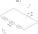
- FIG. 1 is a perspective view of an embodiment of a display device 10.
- FIG. 2 is a plan view showing an embodiment of a display device 10.
- a display device 10 generates and displays moving images or still images.
- the display device 10 may be used as the display screen of portable electronic devices such as a mobile phone, a smart phone, a tablet personal computer (“PC"), a smart watch, a watch phone, a mobile communications terminal, an electronic notebook, an electronic book, a portable multimedia player ("PMP"), a navigation device and a ultra mobile PC (“UMPC”), as well as the display screen of various electronic products such as a television, a notebook, a monitor, a billboard and the Internet of Things (“IoT").
- portable electronic devices such as a mobile phone, a smart phone, a tablet personal computer (“PC”), a smart watch, a watch phone, a mobile communications terminal, an electronic notebook, an electronic book, a portable multimedia player (“PMP”), a navigation device and a ultra mobile PC (“UMPC”)
- PMP portable multimedia player
- UMPC ultra mobile PC
- the display device 10 may be a light-emitting display device such as an organic light-emitting display device using organic light-emitting diodes, a quantum-dot light-emitting display device including a quantum-dot light-emitting layer, an inorganic light-emitting display device including an inorganic semiconductor, and an ultra-small light-emitting display device using micro or nano light-emitting diodes ("LEDs"), such as micro LEDs or nano LEDs.
- LEDs micro or nano light-emitting diodes
- the display device 10 includes a display panel 100, a display driving circuit 200 provided in plural including display driving circuits 200, and a circuit board 300 provided in plural including circuit boards 300.
- the display panel 100 may be provided or formed in a rectangular shape having longer sides along a first direction (x-axis direction) and shorter sides along a second direction (y-axis direction) crossing the first direction (x-axis direction).
- each of the corners where a longer side extended along the first direction (x-axis direction) meets a shorter side extended along the second direction (y-axis direction) may be rounded with a predetermined curvature or may be a right angle.
- the planar shape of the display panel 100 when viewed from the top is not limited to a quadrangular shape, but may be provided or formed in a different polygonal shape, a circular shape or an elliptical shape.
- the display panel 100 may be provided or formed flat, but is not limited thereto.
- the display panel 100 may be provided or formed at left and right ends including a curved portion such as having a constant curvature or a varying curvature.
- the display panel 100 may be provided or formed to be flexible so as to be curvable, bendable, foldable and/or rollable.
- the display panel 100 includes a display area DA where images are generated and/or displayed, light is generated and/or emitted, etc., and a non-display area NDA.
- the images and/or light may not be generated or displayed at the non-display area NDA.
- a substrate SUB (see FIG. 6 ) of the display panel 100 includes a display area DA and non-display area NDA. That is, various components or layers of the display device 10 including a display area DA and a non-display area NDA corresponding to those described above for the display device 10.
- the display area DA may occupy most of the planar area of the display panel 100.
- the display area DA may be disposed at the center of display panel 100.
- pixels may be disposed to display images.
- the non-display area NDA is disposed adjacent to the display area DA.
- the non-display area NDA may be disposed on the outer side of the display area DA and closer to an outer edge of the display device 10.
- the non-display area NDA may surround the display area DA.
- the non-display area NDA may be defined as the border of the display panel 100.
- the non-display area NDA may correspond to a bezel of the display device 10.
- a display pad DP provided in plural including a plurality of display pads DP may be disposed to be connected to the circuit boards 300.
- the display pads DP may be disposed at a same one edge of the display panel 100. In an embodiment, for example, the display pads DP may be disposed at the lower edge of the display panel 100.
- the display pads DP may be electrically connected to signal lines of the display panel 100.
- the circuit boards 300 may be disposed on and corresponding to the display pads DP disposed at one edge of the display panel 100.
- the circuit boards 300 may be attached to the display pads DP using a low-resistance, high-reliability material such as an anisotropic conductive film and/or a self-assembly anisotropic conductive paste ("SAP"). Accordingly, the circuit boards 300 may be electrically connected to signal lines of the display panel 100 by the display pads DP.
- the display panel 100 may receive an electrical signal such as data voltages, supply voltages, scan timing signals, etc. through the circuit boards 300 from outside the display panel 100.
- the circuit boards 300 may be a flexible printed circuit board, a printed circuit board or a flexible film such as a chip on film.
- the display driving circuits 200 may generate electrical signals such as data voltages, supply voltages, scan timing signals, etc.
- the display driving circuits 200 may supply electrical signals such as data voltages, supply voltages, scan timing signals, etc. from outside the display panel 100 to the display panel 100 through the circuit boards 300.
- Each of the display driving circuit 200 may be implemented as an integrated circuit ("IC") and may be attached to a respective one of the circuit boards 300.
- the display driving circuits 200 may be attached to the display panel 100 by chip-on-glass (“COG”) technique, chip-on-plastic (“COP”) technique or ultrasonic bonding.
- COG chip-on-glass
- COP chip-on-plastic
- FIG. 3 is an enlarged plan view showing an embodiment of area A of FIG. 2 .
- FIG. 3 shows only a first power supply line PSL1, a first power supply pad line PSPL provided in plural including first power supply pad lines PSPL, a power supply bridge PSB provided in plural including power supply bridges PSB, a second power supply line PSL2 provided in plural including second power supply lines PSL2, the display pads DP and a demux unit DMXU in the non-display area NDA, driving voltage lines VDL in the display area DA, a common electrode 173, and a circuit board 300.
- the first power supply line PSL1, the first power supply pad lines PSPL, the power supply bridges PSB, the second power supply lines PSL2 and the demux unit DMXU may be disposed in the non-display area NDA.
- the driving voltage lines VDL and the common electrode 173 may be disposed in both the display area DA and the non-display area NDA.
- the first power supply line PSL1 and the demux unit DMXU may be extended along the first direction (x-axis direction).
- the first power supply pad lines PSPL, the power supply bridges PSB and the driving voltage lines VDL may be extended along the second direction (y-axis direction) and spaced apart from each other along the first direction (x-axis direction).
- the first power supply line PSL1 is connected to the driving voltage lines VDL.
- the driving voltage lines VDL may protrude from the upper side of the first power supply line PSL1 along the second direction (y-axis direction).
- the first power supply line PSL1 and the driving voltage lines VDL may together form a power supply member or a driving voltage member.
- Each of the first power supply pad lines PSPL may be connected to a respective one of the display pads DP.
- Each of the first power supply pad lines PSPL of the display panel 100 may receive a first supply voltage of the display driving circuit 200 through the circuit board 300.
- Each of the power supply bridges PSB may connect the first power supply line PSL1 with the first power supply pad line PSPL.
- a first end of the power supply bridge PSB may be connected to the first power supply line PSL1 at or through a first power connection contact hole DCT1.
- a second end of the power supply bridge PSB which is opposite to the first end thereof may be connected to the first power supply pad line PSPL at or through a second power connection contact hole DCT2.
- Each of the power supply bridges PSB may overlap the demux unit DMXU along a third direction (z-axis direction) which crosses bot the (x-axis direction) and the second direction (y-axis direction).
- Each of the second power supply lines PSL2 may be connected to a respective one of the display pads DP.
- the display pads DP to which the first power supply pad lines PSPL and the second power supply lines PSL2 may correspond to a same one of the circuit board 300 without being limited thereto.
- Each of the second power supply lines PSL2 may receive a second supply voltage of the display driving circuit 200 through the circuit board 300.
- the second supply voltage may be a voltage having a lower level than that of the first supply voltage.
- the first supply voltage may be a high-level driving voltage
- the second supply voltage may be a low-level driving voltage.
- each of the second power supply lines PSL2 may be bent at least once to include a bent portion.
- a first one of the second power supply lines PSL2 may be extended along the second direction (y-axis direction), may be bent to the left along the first direction (x-axis direction), and then may be further extended along the first direction (x-axis direction).
- a second one of the second power supply lines PSL2 may be extended along the second direction (y-axis direction), may be bent to the right along the first direction (x-axis direction), and then may be further extended along the first direction (x-axis direction).
- a third one of the second power supply lines PSL2 may be extended in the second direction (y-axis direction), may be bent to the right and extended in the first direction (x-axis direction), and then may be further bent in a direction opposite to the second direction (y-axis direction).
- the third one of the second power supply lines PSL2 may be connected to one of the display pads DP, and an opposing end thereof may be connected to another one of the display pads DP.
- the demux unit DMXU may be disposed between the first power supply line PSL1 and the first power supply pad line PSPL along the second direction (y-axis direction).
- the demux unit DMXU may be disposed between the first power supply line PSL1 and the second power supply line PSL2 along the second direction (y-axis direction).
- the demux unit DMXU may be extended along the first direction (x-axis direction) to dispose a major dimension along the first direction (x-axis direction).
- the demux unit DMXU may include a plurality of demux transistors DMT1 and DMT2 (see FIG. 4 ) for distributing data voltages of a data fan-out line DFL provided in plural including a plurality of data fan-out lines DFL (see FIG. 4 ) to one of a data line DL among a plurality of data lines DL (see FIG. 4 ).
- the demux unit DMXU will be described later with reference to FIG. 4 .
- the common electrode 173 may be disposed in the display area DA and the non-display area NDA.
- the common electrode 173 may overlap the second power supply lines PSL2 along the third direction (z-axis direction).
- the common electrode 173 may be connected to each of the second power supply line PSL2 through a third power connection contact hole DCT3. Accordingly, the second supply voltage may be applied to the common electrode 173.
- FIG. 4 is an enlarged plan view of an embodiment of area B of FIG. 3 .
- FIG. 4 shows only the first power supply line PSL1, the first power supply pad line PSPL, the power supply bridge PSB, the second power supply line PSL2, the data fan-out lines DFL, the demux unit DMXU and the data lines DL, the driving voltage lines VDL and a sub-pixel PX provided in plural including sub-pixels PX of a pixel in the display area DA.
- the data fan-out lines DFL may be connected to the display pads DP (see FIG. 3 ), respectively.
- each of the data fan-out lines DFL may be connected to the display pad DP as a second display pad among the display pads DP (see FIG. 3 ).
- each of the data fan-out lines DFL may receive the data voltage of the display driving circuit 200 through the circuit board 300.
- Each of the data fan-out lines DFL may be bent at least once in the plan view.
- Each of the first power supply pad lines PSPL and the power supply bridge PSB may overlap the data fan-out lines DFL along the third direction (z-axis direction).
- Each of the second power supply lines PSL2 may overlap the data fan-out lines DFL in the third direction (z-axis direction).
- the demux unit DMXU may include a first control line CL1, a second control line CL2, and first and second demux transistors DMT1 and DMT2.
- the first control line CL1 and the second control line CL2 may be extended along the first direction (x-axis direction).
- the first control line CL1 may be connected to the display pad DP as a first display pad among the display pads DP (see FIG. 3 ) to receive a first control signal from the display driving circuit 200.
- the second control line CL2 may also be connected to the display pad DP a first display pad among the display pads DP (see FIG. 3 ) to receive a second control signal from the display driving circuit 200.
- the first demux transistor DMT1 may include a common active layer MACT, a first demux gate electrode MG1, a common source electrode MS and a first demux drain electrode MD1.
- the second demux transistor DMT2 may include a common active layer MACT, a second demux gate electrode MG2, a common source electrode MS and a second demux drain electrode MD2.
- the common active layer MACT may be commonly provided or formed in the first demux transistor DMT1 and the second demux transistor DMT2.
- the common active layer MACT may overlap the first demux drain electrode MD1, the first demux gate electrode MG1, the common source electrode MS, the second demux gate electrode MG2 and the second demux drain electrode MD2 along the third direction (z-axis direction).
- the first demux gate electrode MG1 may be connected to the first control line CL1 through a first contact hole CT1.
- the first demux gate electrode MG1 may be disposed between the first demux drain electrode MD1 and the common source electrode MS along the first direction (x-axis direction).
- the first demux gate electrode MG1 may include a major dimension extended along the second direction (y-axis direction).
- the second demux gate electrode MG2 may be connected to the second control line CL2 through a second contact hole CT2.
- the second demux gate electrode MG2 may be disposed between the common source electrode MS and the second demux drain electrode MD2 along the first direction (x-axis direction).
- the second demux gate electrode MG2 may include a major dimension extended along the second direction (y-axis direction).
- the common source electrode MS may be commonly provided or formed in the first demux transistor DMT1 and the second demux transistor DMT2.
- the common source electrode MS may be connected to the data fan-out line DFL through a third contact hole CT3.
- the common source electrode MS may be connected to the common active layer MACT through a fourth contact hole CT4.
- the common source electrode MS may include a major dimension extended along the second direction (y-axis direction).
- the first demux drain electrode MD1 may be connected to the common active layer MACT through a fifth contact hole CT5 provided in plural including a plurality of fifth contact holes CT5.
- the first demux drain electrode MD1 may be connected to a first data bridge DB1 through a first bridge contact hole BCT1.
- the first demux drain electrode MD1 may include a major dimension extended along the second direction (y-axis direction).
- the second demux drain electrode MD2 may be connected to the common active layer MACT through a sixth contact hole CT6 provided in plural including a plurality of sixth contact holes CT6.
- the second demux drain electrode MD2 may be connected to a second data bridge DB2 through a third bridge contact hole BCT3.
- the second demux drain electrode MD2 may include a major dimension extended along the second direction (y-axis direction).
- the first data bridge DB1 may connect the first demux drain electrode MD1 of the first demux transistor DMT1 with the data line DL.
- a first end of the first data bridge DB1 may be connected to the first demux drain electrode MD1 at or through the first bridge contact hole BCT1, and a second end opposite to the first end thereof may be connected to the data line DL at or through the second bridge contact hole BCT2.
- the first data bridge DB1 may overlap the first power supply line PSL1 along the third direction (z-axis direction).
- the first data bridge DB1 may cross the first power supply line PSL1.
- the first data bridge DB1 may include a major dimension extended along the second direction (y-axis direction).
- the second data bridge DB2 may connect the second demux drain electrode MD2 of the second demux transistor DMT2 with the data line DL.
- a first end of the second data bridge DB2 may be connected to the second demux drain electrode MD2 at or through the third bridge contact hole BCT3, and a second end opposite to the first end thereof may be connected to the data line DL at or through the fourth bridge contact hole BCT4.
- the second data bridge DB2 may overlap the first power supply line PSL1 along the third direction (z-axis direction).
- the second data bridge DB2 may cross the first power supply line PSL1.
- the second data bridge DB2 may include a major dimension extended along the second direction (y-axis direction).
- the data line DL (e.g., first data line) connected to the first data bridge DB1 may receive the data voltage of the data fan-out line DFL.
- the data line DL (e.g., second data line) connected to the second data bridge DB2 may receive the data voltage of the data fan-out line DFL.
- the first and second demux transistors DMT1 and DMT2 may apply the data voltages of a same one of the data fan-out line DFL to a plurality of data lines DL at different timings, and thus reducing the number of the data fan-out lines DFL and the number of the display pads DP is possible.
- the power supply bridge PSB may connect the first power supply line PSL1 with the first power supply pad line PSPL by avoiding electrical connection with the demux transistors DMT1 and DMT2 of the demux unit DMXU.
- the power supply bridge PSB may overlap the plurality of demux transistors DMT1 and DMT2 along the third direction (z-axis direction).
- the sub-pixels PX may be arranged in a matrix along the first direction (x-axis direction) and along the second direction (y-axis direction). Each of the sub-pixels PX may be electrically connected to a data line DL and a driving voltage line VDL disposed on one side (e.g., left or right hand) thereof. Accordingly, each of the sub-pixels PX may control the electrical current flowing from the first supply voltage of the driving voltage line VDL to a light-emitting element LEL based on the data voltage applied from the data line DL, thereby adjusting the luminance of light generated and/or emitted from the light-emitting element LEL. Each of the sub-pixels PX will be described later with reference to FIG. 5 .
- the sub-pixels PX are disposed between the driving voltage line VDL and the data line DL along the first direction (x-axis direction) in FIG. 4 , the invention is not limited thereto. In an embodiment, for example, the sub-pixels PX may overlap at least one of the driving voltage line VDL and the data line DL along the third direction (z-axis direction).
- a dimension along the second direction (y-axis direction) is decreased, and thus a corresponding dimension (e.g., a width) of the first power supply line PSL1 along the second direction (y-axis direction) is reduced.
- the electrical resistance of the first power supply line PSL1 increases, and thus deviations in electrical resistance between the driving voltage lines VDL connected to the first power supply line PSL1 may increase.
- one or more embodiment provides a display device 10 having increased uniformity in luminance of the pixels of the display device 10 without increasing the dimension (e.g., the width) of the first power supply line PSL1.
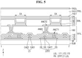
- FIG. 5 is an enlarged cross-sectional view showing an embodiment of the sub-pixels PX taken along line I - I' of FIG. 4 .
- each of the sub-pixels PX may include at least one of a display transistor DTFT, a capacitor C1 and a light-emitting element LEL.
- the display transistor DTFT as a thin-film transistor is connected to the light-emitting element LEL.
- a substrate SUB may include or be made of an insulating material such as a polymer resin and glass.
- the substrate SUB may include polyimide.
- the substrate SUB may be a flexible substrate that is bendable, foldable or rollable.
- a thin-film transistor layer TFTL including a display transistor DTFT as a thin-film transistor, and a capacitor C1, of each of the sub-pixels PX may be disposed on the substrate SUB.
- the thin-film transistor layer TFTL may include the display transistor DTFT, an anode connection electrode ANDE, a buffer layer BF, a gate insulating layer 130, a first interlayer dielectric layer 141, a second interlayer dielectric layer 142 and a planarization layer 160.
- the buffer layer BF may be disposed on the substrate SUB.
- the buffer layer BF may include be formed of a silicon nitride layer, a silicon oxynitride layer, a silicon oxide layer, a titanium oxide layer or an aluminum oxide layer.
- the display transistor DTFT may be disposed on the buffer layer BF.
- the display transistor DTFT may include a display active layer DACT, a display gate electrode DG, a display source electrode DS and a display drain electrode DD.
- the gate insulating layer 130 may be disposed on the display active layer DACT, the display source electrode DS and the display drain electrode DD of the display transistor DTFT.
- the gate insulating layer 130 may include or be formed of an inorganic layer, for example, a silicon nitride layer, a silicon oxynitride layer, a silicon oxide layer, a titanium oxide layer or an aluminum oxide layer.
- the display gate electrode DG of the display transistor DTFT and a first capacitor electrode CAE1 may be disposed on the gate insulating layer 130.
- the display gate electrode DG may overlap the display active layer DACT along the third direction (z-axis direction).
- the first capacitor electrode CAE1 may overlap a second capacitor electrode CAE2 along the third direction (z-axis direction).
- the display gate electrode DG may include or be made of a single layer or multiple layers among molybdenum (Mo), aluminum (Al), chromium (Cr), gold (Au), titanium (Ti), nickel (Ni), neodymium (Nd) and copper (Cu) and an alloy thereof.
- the first interlayer dielectric layer 141 may be disposed on the display gate electrode DG and the first capacitor electrode CAE1.
- the first interlayer dielectric layer 141 may include or be formed of an inorganic layer, for example, a silicon nitride layer, a silicon oxynitride layer, a silicon oxide layer, a titanium oxide layer or an aluminum oxide layer.
- the second capacitor electrode CAE2 may be disposed on the first interlayer dielectric layer 141. Since the first interlayer dielectric layer 141 has a predetermined dielectric constant, a capacitor C1 can be provided by formed by the first capacitor electrode CAE1, the second capacitor electrode CAE2, and the first interlayer dielectric layer 141 disposed between the first capacitor electrode CAE1 and the second capacitor electrode CAE2.
- the second capacitor electrode CAE2 may include or be made of a single layer or multiple layers of one of molybdenum (Mo), aluminum (Al), chromium (Cr), gold (Au), titanium (Ti), nickel (Ni), neodymium (Nd) and copper (Cu) or an alloy thereof.
- a second interlayer dielectric layer 142 may be disposed over the second capacitor electrode CAE2.
- the second interlayer dielectric layer 142 may include or be formed of an inorganic layer, for example, a silicon nitride layer, a silicon oxynitride layer, a silicon oxide layer, a titanium oxide layer or an aluminum oxide layer.
- the anode connection electrode ANDE may be disposed on the second interlayer dielectric layer 142.
- the anode connection electrode ANDE may be connected to the display drain electrode DD at or through a first anode contact hole ANCT1 that penetrates the first interlayer dielectric layer 141 and the second interlayer dielectric layer 142 to expose the display drain electrode DD of the display transistor DTFT to outside the first interlayer dielectric layer 141 and the second interlayer dielectric layer 142.
- the anode connection electrode ANDE may include or be made of a single layer or multiple layers among molybdenum (Mo), aluminum (Al), chromium (Cr), gold (Au), titanium (Ti), nickel (Ni), neodymium (Nd) and copper (Cu) and an alloy thereof.
- Mo molybdenum
- Al aluminum
- Cr chromium
- Au gold
- Ti titanium
- Ni nickel
- Nd neodymium
- Cu copper
- the planarization layer 160 provides a flat surface over the anode connection electrode ANDE.
- the planarization layer 160 may include or be formed of an organic layer such as an acryl resin, an epoxy resin, a phenolic resin, a polyamide resin and a polyimide resin.
- An emission material layer EML may be disposed on the planarization layer 160.
- the emission material layer EML may include the light-emitting element LEL provided in plural including light-emitting elements LEL and a bank 180.
- Each of the light-emitting elements LEL includes a pixel electrode 171 (e.g., a first electrode), an emissive layer 172 and a common electrode 173 (e.g., a second electrode).
- the common electrode 173 may be commonly connected to the plurality of light-emitting elements LEL.
- the pixel electrode 171 may be provided or formed on the planarization layer 160.
- the pixel electrode 171 may be connected to the anode connection electrode ANDE at or through a second anode contact hole ANCT2 that penetrates the planarization layer 160 and exposes the anode connection electrode ANDE to outside the planarization layer 160.
- the pixel electrode 171 may include or be made of a metal material having a high reflectivity such as a stack structure of aluminum and titanium (Ti / Al / Ti), a stack structure of aluminum and ITO (ITO / Al / ITO), an APC alloy and a stack structure of APC alloy and ITO (ITO / APC / ITO).
- the APC alloy is an alloy of silver (Ag), palladium (Pd) and copper (Cu).
- the bank 180 on the planarization layer 160 may define an opening therein which corresponds to an emission area EA and exposes a portion of the pixel electrode 171 to outside the bank 180.
- the pixel electrode 171, the emissive layer 172 and the common electrode 173 are stacked on one another sequentially in order from the substrate SUB, so that holes from the pixel electrode 171 and electrons from the common electrode 173 are combined with each other in the emissive layer 172 to generate and emit light.
- a solid portion of the bank 180 may cover an edge of the pixel electrode 171.
- the bank 180 may include or be formed of an organic layer such as an acryl resin, an epoxy resin, a phenolic resin, a polyamide resin and a polyimide resin.
- the emissive layer 172 is provided or formed on the pixel electrode 171 and the bank 180.
- the emissive layer 172 may include an organic material and emit light of a certain color.
- the emissive layer 172 may include a hole transporting layer, an organic material layer and an electron transporting layer.
- the common electrode 173 is provided or formed on the emissive layer 172.
- the common electrode 173 faces the pixel electrode 171 with the emissive layer 172 therebetween.
- the common electrode 173 may be provided or formed to cover the emissive layer 172.
- the common electrode 173 may be a common layer provided or formed across all of the emission areas EA.
- the common electrode 173 may be in the opening defined in the bank 180 and along a side surface of the bank 180 to extend outside the opening and along an upper surface of the bank 180.
- a capping layer CPL may be provided or formed on the common electrode 173.
- the common electrode 173 may include or be formed of a transparent conductive oxide (“TCO”) such as indium tin oxide (“ITO”) and indium zinc oxide (“IZO”) that can transmit light, or a semi-transmissive conductive material such as magnesium (Mg), silver (Ag) and an alloy of magnesium (Mg) and silver (Ag).
- TCO transparent conductive oxide
- ITO indium tin oxide
- IZO indium zinc oxide
- An encapsulation layer TFEL may be disposed on the common electrode 173.
- the encapsulation layer TFEL includes at least one inorganic layer to reduce or effectively prevent permeation of oxygen or moisture into the emission material layer EML.
- the encapsulation layer TFEL includes at least one organic layer to protect the light-emitting element layer EML from foreign substances such as dust.
- the encapsulation layer TFEL may include a first inorganic layer TFE1, an organic layer TFE2 and a second inorganic layer TFE3.
- the first inorganic layer TFE1 may be disposed on the common electrode 173, the organic layer TFE2 may be disposed on the first inorganic layer TFE1, and the second inorganic layer TFE3 may be disposed on the organic layer TFE2.
- the first inorganic layer TFE1 and the second inorganic layer TFE3 may include or be made of multiple layers in which one or more inorganic layers of a silicon nitride layer, a silicon oxynitride layer, a silicon oxide layer, a titanium oxide layer and an aluminum oxide layer are alternately stacked on one another.
- the organic layer TFE2 may include or be formed of acryl resin, an epoxy resin, a phenolic resin, a polyamide resin, a polyimide resin, etc.
- a filling layer, a sealing material and/or an encapsulation substrate may be disposed to prevent permeation of oxygen or moisture into the emission material layer EML and/or protect the light-emitting element layer EML from foreign substances.
- the encapsulation substrate may be an insulating substrate including an insulating material such as glass and plastic.
- the filling layer may be, but is not limited to, an air layer in a vacuum state.
- the sealing material may be disposed in the non-display area NDA (see FIGS. 1 and 2 ) of the display panel 100 and may surround the display area DA in the plan view.
- FIG. 6 is an enlarged cross-sectional view showing an embodiment of a display panel 100 taken along line II - II' of FIG. 4 .
- FIG. 7 is an enlarged cross-sectional view showing an embodiment of the display panel 100 taken along line III - III' of FIG. 4 .
- FIG. 8 is an enlarged cross-sectional view showing an embodiment of the display panel 100 taken along lines IV - IV' and V - V' of FIG. 4 .
- the common active layer MACT of the first demux transistor DMT1 may be disposed on the buffer layer BF.
- the gate insulating layer 130 may be disposed on the common active layer MACT.
- the common active layer MACT may be disposed on the same layer as the display active layer DACT of the display transistor DTFT and may include or be formed of the same material.
- the common active layer MACT of the first demux transistor DMT1 may be disposed in a same layer as the display active layer DACT of the display transistor DTFT. As being in a same layer, elements may be respective patterns of a same material layer.
- the common active layer MACT in the non-display area NDA and the display active layer DACT of the display area DA may be respective patterns of a same material layer on the substrate SUB.
- elements which are provided or formed simultaneously may also be in a same layer as each other.
- the first demux gate electrode MG1 of the first demux transistor DMT1, the data fan-out line DFL, and the first data bridge DB1 may be disposed on the gate insulating layer 130.
- the second demux gate electrode MG2 (see FIG. 4 ) and the second data bridge DB2 (see FIG. 4 ) may also be disposed on the gate insulating layer 130.
- the first interlayer dielectric layer 141 may be disposed on the first demux gate electrode MG1, the second demux gate electrode MG2 (see FIG. 4 ), the data fan-out line DFL, the second data bridge DB2 (see FIG. 4 ), and the first data bridge DB1.
- the first demux gate electrode MG1, the second demux gate electrode MG2 see FIG.
- the data fan-out line DFL, the second data bridge DB2 (see FIG. 4 ) and the first data bridge DB1 may be disposed on the same layer as the display gate electrode DG and the first capacitor electrode CAE1 of the display transistor DTFT and may include or be formed of the same material.
- the first demux gate electrode MG1, the second demux gate electrode MG2, the data fan-out line DFL, the second data bridge DB2 and the first data bridge DB1 of the non-display area NDA may be in a same layer as the display gate electrode DG and the first capacitor electrode CAE1 of the display area DA.
- the first power supply line PSL1 includes a first sub-power supply line SPSL1 (e.g., first sub-power supply line layer) and a second sub-power supply line SPSL2 (e.g., second sub-power supply line layer).
- the second sub-power supply line SPSL2 is disposed on the first sub-power supply line SPSL1.
- the second sub-power supply line SPSL2 may be further from the substrate SUB than the first sub-power supply line SPSL1.
- the second sub-power supply line SPSL2 extends along the upper side and the side surfaces of the first sub-power supply line SPSL1.
- the second width W2 of the second sub-power supply line SPSL2 may be larger than the first width W1 of the first sub-power supply line SPSL1.
- the second sub-power supply line SPSL2 extends further than the first sub-power supply line SPSL1 to define an extended portion of the second sub-power supply line SPSL2.
- the widths may indicate a maximum dimension of the respective supply line.
- the first width W1 of the first sub-power supply line SPSL1 may refer to a minor dimension of the first sub-power supply line SPSL1 along the second direction (y-axis direction), and the second width W2 of the second sub-power supply line SPSL2 may refer to a minor dimension of the second sub-power supply line SPSL2 along the second direction (y axis direction).
- the second sub-power supply line SPSL2 may cover the first sub-power supply line SPSL1.
- the second sub-power supply line SPSL2 may be in contact with the first sub-power supply line SPSL1. As being in contact (e.g., physical contact), elements may form an interface therebetween.
- the first power supply pad line PSPL may include a first sub-power supply pad line PSPL1 and a second sub-power supply pad line PSPL2.
- the second sub-power supply pad line PSPL2 may be disposed on the first sub-power supply pad line PSPL1.
- the second sub-power supply pad line PSPL2 may extend along the upper surface and side surfaces of the first sub-power supply pad line PSPL1.
- the fourth width W4 of the second sub-power supply pad line PSPL2 may be larger than the third width W3 of the first sub-power supply pad line PSPL1.
- the third width W3 of the first sub-power supply pad line PSPL1 may refer to a minor dimension of the first sub-power supply line SPSL1 along the first direction (x-axis direction)
- the fourth width W4 of the second sub-power supply line SPSL2 may refer to a minor dimension of the second sub-power supply line SPSL2 along the first direction (x axis direction).
- the second sub-power supply pad line PSPL2 may cover the first sub-power supply pad line PSPL1.
- the second sub-power supply pad line PSPL2 may be in contact with the first sub-power supply pad line PSPL1.
- the driving voltage line VDL may protrude from the second sub-power supply line SPSL2. That is, the second sub-power supply line SPSL2 may define the driving voltage line VDL. Referring to FIG. 6 , for example, the driving voltage line VDL may include only the layer of the second sub-power supply line SPSL2 and may exclude the layer of the first sub-power supply line SPSL1.
- the first power supply line PSL1, the first power supply pad line PSPL, the first control line CL1, the second control line CL2, the driving voltage line VDL and the common source electrode MS and the first demux drain electrode MD1 of the first demux transistor DMT1 may be disposed on the second interlayer dielectric layer 142.
- the common source electrode MS and the second demux drain electrode MD2 of the second demux transistor DMT2 may also be disposed on the second interlayer dielectric layer 142. That is, these elements on the second interlayer dielectric layer 142 may be in a same layer as each other.
- the planarization layer 160 may be disposed on the first power supply line PSL1, the first power supply pad line PSPL, the first control line CL1, the second control line CL2, the driving voltage line VDL, the common source electrode MS and the first demux drain electrode MD1 of the first demux transistor DMT1, and the common source electrode MS and the second demux drain electrode MD2 of the second demux transistor DMT2.
- the second sub-power supply line SPSL2 of the first power supply line PSL1, the second sub-power supply pad line PSPL2 of the first power supply pad line PSPL, the first control line CL1, the second control line CL2, the driving voltage line VDL, and the common source electrode MS and the first demux drain electrode MD1 of the first demux transistor DMT1 may include or be made of the same material as the anode connection electrode ANDE. That is, second sub-power supply line SPSL2, the second sub-power supply pad line PSPL2, the first control line CL1, the second control line CL2, the driving voltage line VDL and the common source electrode MS in the non-display area NDA may be in a same layer as the anode connection electrode ANDE in the display area DA.
- the first sub-power supply line SPSL1 of the first power supply line PSL1 and the first sub-power supply pad line PSPL1 of the first power supply pad line PSPL may include or be made of either the same material as or a different material from the anode connection electrode ANDE.
- the first sub-power supply line SPSL1 of the first power supply line PSL1 and the first sub-power supply pad line PSPL1 of the first power supply pad line PSPL may include or be made of a single layer or multiple layers among molybdenum (Mo), aluminum (Al), chromium (Cr), gold (Au), titanium (Ti), nickel (Ni), neodymium (Nd) and copper (Cu) and an alloy thereof.
- the common source electrode MS may be connected to the data fan-out line DFL through a third contact hole CT3 penetrating the first interlayer dielectric layer 141 and the second interlayer dielectric layer 142.
- the common source electrode MS may be connected to the common active layer MACT through a fourth contact hole CT4 penetrating the gate insulating layer 130, the first interlayer dielectric layer 141 and the second interlayer dielectric layer 142.
- the first demux drain electrode MD1 may be connected to the common active layer MACT through a fifth contact hole CT5 penetrating the gate insulating layer 130, the first interlayer dielectric layer 141 and the second interlayer dielectric layer 142.
- the first demux drain electrode MD1 may be connected to the first data bridge DB1 through a first bridge contact hole BCT1 penetrating the first interlayer dielectric layer 141 and the second interlayer dielectric layer 142.
- the power supply bridge PSB may be disposed on the planarization layer 160.
- the bank 180 may be disposed on the power supply bridge PSB.
- the power supply bridge PSB may be disposed on the same layer as the pixel electrode 171 and may include or be made of the same material.
- the power supply bridge PSB may be connected to the second sub-power supply line SPSL2 of the first power supply line PSL1 through a first power connection contact hole DCT1 penetrating the planarization layer 160.
- the power supply bridge PSB may be connected to the second sub-power supply pad line PSPL2 of the first power supply pad line PSPL through a second power connection contact hole DCT2 penetrating the planarization layer 160.
- the first power supply line PSL1 includes the first sub-power supply line SPSL1 and the second sub-power supply line SPSL2, and the first power supply pad line PSPL may include the first sub-power supply pad line PSPL1 and the second sub-power supply pad line PSPL2.
- the first power supply line PSL1 and the first power supply pad line PSPL may have a two-layer wiring structure. Accordingly, even though the planar area of the non-display area NDA of the display device 10 is reduced and accordingly the width of the first power supply line PSL1 is reduced, increasing of electrical resistance of the first power supply line PSL1 may be reduced or effectively prevented.
- FIG. 9 is an enlarged cross-sectional view showing area C of FIG. 8 in detail.
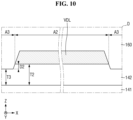
- FIG. 10 is an enlarged cross-sectional view showing area D of FIG. 8 in detail.
- a thickness of the second interlayer dielectric layer 142 may vary in a direction along the substrate SUB.
- the first area A1 of the second interlayer dielectric layer 142 corresponds to a region where the second interlayer dielectric layer 142 and the first sub-power supply line SPSL1 overlap each other along the third direction (z-axis direction).
- the second area A2 of the second interlayer dielectric layer 142 includes a region where the second interlayer dielectric layer 142 overlaps only with the second sub-power supply line SPSL2 along the third direction (z-axis direction).
- the third area A3 of the second interlayer dielectric layer 142 includes a region where the second interlayer dielectric layer 142 does not overlap with the first power supply line PSL1 along the third direction (z-axis direction) since the first power supply line PSL1 is omitted at the third area A3.
- the second interlayer dielectric layer 142 may have a first thickness T1 at the first area A1, a second thickness T2 at the second area A2 which is smaller than the first thickness T1, and a third thickness T3 at the third area A3 which is smaller than the second thickness T2.
- the thicknesses of the second interlayer dielectric layer 142 may be defined as a minimum distance from the upper surface of the first interlayer dielectric layer 141 which is furthest from the substrate SUB along the third direction (z-axis direction) to the upper surface of the second interlayer dielectric layer 142 which is furthest from the substrate SUB along the third direction (z-axis direction).
- the first thickness T1 of the second interlayer dielectric layer 142 corresponding to the first sub-power supply line SPSL1 along the third direction (z-axis direction) may be larger than the second thickness T2 of the second interlayer dielectric layer 142 corresponding not with the first sub-power supply line SPSL1 but with only the second sub-power supply line SPSL2 along the third direction (z-axis direction).
- the second thickness T2 of the second interlayer dielectric layer 142 overlapping not with the first sub-power supply line SPSL1 but with only the second sub-power supply line SPSL2 along the third direction (z-axis direction) may be larger than the third thickness T3 along the third direction (z-axis direction) of the second interlayer dielectric layer 142 which is outside of the first power supply line PSL1 in a plan view and in a direction along the substrate SUB.
- the second area A2 of the second interlayer dielectric layer 142 may further include a region where the second interlayer dielectric layer 142 overlaps with the driving voltage line VDL along the third direction (z-axis direction).
- the third area A3 of the second interlayer dielectric layer 142 may further include a region where the second interlayer dielectric layer 142 does not overlap with the driving voltage line VDL along the third direction (z-axis direction). That is, the third area A3 may be outside the driving voltage line VDL in a direction along the substrate SUB.
- the second thickness T2 of the second interlayer dielectric layer 142 which corresponds to the driving voltage line VDL along the third direction (z-axis direction) may be larger than the third thickness T3 of the second interlayer dielectric layer 142 does not correspond with the driving voltage line VDL along the third direction (z-axis direction).
- the second thickness T2 of the second interlayer dielectric layer 142 overlapping with the driving voltage line VDL along the third direction (z-axis direction) may be smaller than the first thickness T1 of the second interlayer dielectric layer 142 overlapping with the first sub-power supply line SPSL1 along the third direction (z-axis direction).
- the second thickness T2 of the second interlayer dielectric layer 142 overlapping with the driving voltage line VDL along the third direction (z-axis direction) may be smaller than the second thickness T2 of the second interlayer dielectric layer 142 overlapping not with the first sub-power supply line SPSL1 but with the second sub-power supply line SPSL2 along the third direction (z-axis direction) ( FIG. 9 ).
- the third thickness T3 of the second interlayer dielectric layer 142 not overlapping with the driving voltage line VDL along the third direction (z-axis direction) ( FIG. 10 ) may be substantially equal to the third thickness T3 of the second interlayer dielectric layer 142 not overlapping with the first power supply line PSL1 along the third direction (z-axis direction) ( FIG. 9 ).
- the second area A2 of the second interlayer dielectric layer 142 further includes regions where the second interlayer dielectric layer 142 overlaps along the third direction (z-axis direction) with the anode connection electrode ANDE (see FIG. 5 ), the first control line CL1 (see FIG. 6 ), the second control line CL2 (see FIG. 6 ), the common source electrode MS (see FIG. 6 ), the first demux drain electrode MD1 (see FIG. 6 ) and the second demux drain electrode MD2 (see FIG. 5 ) which are provided or formed in a same layer such as to include of a same material as the driving voltage line VDL.
- the third area A3 of the second interlayer dielectric layer 142 further includes regions where the second interlayer dielectric layer 142 does not overlap along the third direction (z-axis direction) with the anode connection electrode ANDE (see FIG. 5 ), the first control line CL1 (see FIG. 6 ), the second control line CL2 (see FIG. 6 ), the common source electrode MS (see FIG. 6 ), the first demux drain electrode MD1 (see FIG. 6 ) and the second demux drain electrode MD2 (see FIG. 5 ).
- the thicknesses of the second interlayer dielectric layer 142 in the first to third areas A1, A2 and A3 will be further described with reference to FIGS. 26 to 37 .
- FIG. 11 is an enlarged cross-sectional view showing an embodiment of the display panel 100 taken along line VI - VI' of FIG. 4 .
- the second power supply line PSL2 may be disposed on the second interlayer dielectric layer 142.
- the planarization layer 160 may be disposed on the second power supply line PSL2.
- the second power supply line PSL2 may include or be made of the same material as the anode connection electrode ANDE, the second sub-power supply line SPSL2 of the first power supply line PSL1, the second sub-power supply pad line PSPL2 of the first power supply pad line PSPL, the first control line CL1, the second control line CL2, the driving voltage line VDL, and the common source electrode MS and the first demux drain electrode MD1 of the first demux transistor DMT1.
- the second power supply line PSL2 may include or be made of either the same material as or a different material from the first sub-power supply line SPSL1 of the first power supply line PSL1 and the first sub-power supply pad line PSPL1 of the first power supply pad line PSPL.
- the thickness of the second interlayer dielectric layer 142 corresponding to the second power supply line PSL2 along the third direction (z-axis direction) may be substantially equal to the second thickness T2 of the second interlayer dielectric layer 142 corresponding to the driving voltage line VDL along the third direction (z-axis direction) as in FIG. 10 .
- FIG. 12 is an enlarged cross-sectional view showing an embodiment of the display panel 100 taken along line VI - VI' of FIG. 4 .
- the second power supply line PSL2 may include a third sub-power supply line SPSL3 and a fourth sub-power supply line SPSL4.
- the fourth sub-power supply line SPSL4 may be disposed on the third sub-power supply line SPSL3.
- the fourth sub-power supply line SPSL4 may be extended along the upper side and the side surfaces of the third sub-power supply line SPSL3.
- the width of the fourth sub-power supply line SPSL4 may be larger than the width of the third sub-power supply line SPSL3.
- the fourth sub-power supply line SPSL4 may cover the third sub-power supply line SPSL3.
- the fourth sub-power supply line SPSL4 may be in contact with the third sub-power supply line SPSL3.
- the thickness of the second interlayer dielectric layer 142 which corresponds to the third sub-power supply line SPSL3 of the second power supply line PSL2 along the third direction (z-axis direction) may be substantially equal to the first thickness T1 of the second interlayer dielectric layer 142 corresponding to the first sub-power supply line SPSL1 of the first power supply line PSL1 along the third direction (z-axis direction) as in FIG. 9 .
- the thickness of the second interlayer dielectric layer 142 overlapping not with the third sub-power supply line SPSL3 but with the fourth sub-power supply line SPSL4 along the third direction (z-axis direction) may be substantially equal to the second thickness T2 of the second interlayer dielectric layer 142 overlapping not with the first sub-power supply line SPSL1 but with the second sub-power supply line SPSL2 along the third direction (z-axis direction).
- FIG. 13 is a flowchart for illustrating an embodiment of a method of providing or fabricating a display device 10.
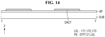
- FIGS. 14 to 25 are cross-sectional views for illustrating embodiments of structures in the method of provided or fabricating a display device 10.
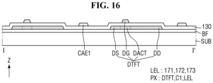
- a buffer layer BF is provided or formed on a substrate SUB, and a display active layer DACT of a display transistor DTFT is provided or formed on the buffer layer BF (S100 of FIG. 13 ).
- the buffer layer BF is provided or formed by depositing an inorganic material on the substrate SUB. Subsequently, the display active layer DACT and a common active layer MACT (see FIG. 6 ) of the first demux transistor DMT1 (see FIG. 6 ) and a second demux transistor DMT2 (see FIG. 4 ) are provided or formed on the buffer layer BF such as by using a photolithography process. In an embodiment, the display active layer DACT and the common active layer MACT (see FIG. 6 ) of the first demux transistor DMT1 (see FIG. 6 ) and the second demux transistor DMT2 (see FIG. 4 ) may be provided or formed simultaneously.
- a gate insulating layer 130 is provided or formed on the display active layer DACT, and a display gate electrode DG of the display transistor DTFT is provided or formed on the gate insulating layer 130 (S200 of FIG. 13 ).
- the gate insulating layer 130 is provided or formed by depositing an inorganic material on the display active layer DACT. Subsequently, the display gate electrode DG, a first capacitor electrode CAE1, a first demux gate electrode MG1 of the first demux transistor DMT1 (see FIG. 6 ), and a second demux gate electrode MG2 of the second demux transistor DMT2 (see FIG. 4 ) are provided or formed on the gate insulating layer 130 such as by using a photolithography process. In an embodiment, the display gate electrode DG, the first capacitor electrode CAE1, the first demux gate electrode MG1 of the first demux transistor DMT1 (see FIG. 6 ) and the second demux gate electrode MG2 of the second demux transistor DMT2 (see FIG. 4 ) may be provided or formed simultaneously.
- Portions of the display active layer DACT may be doped with ions or impurities to have electrical conductivity. Accordingly, the display source electrode DS and the display drain electrode DD having electrical conductivity may be provided or formed.
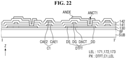
- a first interlayer dielectric layer 141 is provided or formed on the display gate electrode DG, and a second capacitor electrode CAE2 is provided or formed on the first interlayer dielectric layer 141 (S300 of FIG. 13 ).
- the first interlayer dielectric layer 141 is provided or formed by depositing an inorganic material on the display gate electrode DG.
- the second capacitor electrode CAE2 is provided or formed on the first interlayer dielectric layer 141 such as by using a photolithography process.
- a second interlayer dielectric layer 142 is provided or formed on the second capacitor electrode CAE2, and the first sub-power supply line SPSL1 of the first power supply line PSL1 is provided or formed on the second interlayer dielectric layer 142 (S400 of FIG. 13 ).
- an inorganic material is deposited on the second capacitor electrode CAE2 to provided or form the second interlayer dielectric layer 142.
- the first sub-power supply line SPSL1 of the first power supply line PSL1 and the first sub-power supply pad line PSPL1 (see FIG. 7 ) of the first power supply pad line PSPL (see FIG. 7 ) are provided or formed on the second interlayer dielectric layer 142 such as by using a photolithography process.
- the third sub-power supply line SPSL3 may be provided or formed simultaneously with the first sub-power supply line SPSL1 of the first power supply line PSL1 and the first sub-power supply pad line PSPL1 (see FIG. 7 ) of the first power supply pad line PSPL (see FIG. 7 ).
- an anode connection electrode ANDE and a driving voltage line VDL are provided or formed on the second interlayer dielectric layer 142, and at the same time, the second sub-power supply line SPSL2 is provided or formed on the first sub-power supply line SPSL1 (S500 of FIG. 13 ).
- the anode connection electrode ANDE, the driving voltage line VDL, a first demux drain electrode MD1 (see FIG. 6 ) of the first demux transistor DMT1 (see FIG. 6 ), a second demux drain electrode MD2 (see FIG. 5 ) of the second demux transistor DMT2 (see FIG. 4 ) and a common source electrode MS are provided or formed on the second interlayer dielectric layer 142 such as using a photolithography process, a second sub-power supply line SPSL2 is provided or formed on the first sub-power supply line SPSL1, and a second sub-power supply pad line PSPL2 is provided or formed on the first sub-power supply pad line PSPL1.
- the fourth sub-power supply line SPSL4 may be provided or formed simultaneously with the second sub-power supply line SPSL2 of the second power supply line PSL2 and the second sub-power supply pad line PSPL2 of the second power supply pad line PSPL.
- a planarization layer 160 is provided or formed on the anode connection electrode ANDE, the driving voltage line VDL and the second sub-power supply line SPSL2, and a light-emitting element LEL including a pixel electrode 171, an emissive layer 172 and a common electrode 173 is provided or formed on the planarization layer 160 (S600 of FIG. 13 ).
- an organic material is deposited on the anode connection electrode ANDE, the driving voltage line VDL, the second sub-power supply line SPSL2, the first demux drain electrode MD1 (see FIG. 6 ) of the first demux transistor DMT1 (see FIG. 6 ), the second demux drain electrode MD2 (see FIG. 5 ) of the second demux transistor DMT2 (see FIG. 4 ) and the common source electrode MS, to provide or form the planarization layer 160.
- the pixel electrode 171 is provided or formed on the planarization layer 160 such as by using a photolithography process.
- a bank 180 is provided or formed on the pixel electrode 171 such as by using a photolithography process.
- the emissive layer 172 is provided or formed on the bank 180 such as by using a deposition process using a mask.
- the common electrode 173 is provided or formed on the emissive layer 172 such as by using a photolithography process.
- An inorganic material is deposited on the common electrode 173 to provide or form a first inorganic layer TFE1 of an encapsulation layer TFEL. Subsequently, an organic material is deposited on the first inorganic layer TFE1 to provide or form an organic layer TFE2 of the encapsulation layer TFEL. Subsequently, an inorganic material is deposited on the organic layer TFE2 to provide or form a second inorganic layer TFE3 of the encapsulation layer TFEL.
- the first power supply line PSL1 includes the first sub-power supply line SPSL1 and the second sub-power supply line SPSL2, and the first power supply pad line PSPL (see FIG. 7 ) may include the first sub-power supply pad line PSPL1 (see FIG. 7 ) and the second sub-power supply pad line PSPL2 (see FIG. 7 ).
- the first power supply line PSL1 and the first power supply pad line PSPL may have a two-layer wiring structure.
- the planar area of the non-display area NDA of the display device 10 is reduced and accordingly the width of the first power supply line PSL1 is reduced, increasing of the electrical resistance of the first power supply line PSL1 is reduced or effectively prevented. Therefore, increasing of electrical resistance between the driving voltage lines VDL connected to the first power supply line PSL1 is suppressed or effectively prevented. Accordingly, non-uniformity of the luminance of the pixels of the display device 10 may be suppressed or effectively prevented.
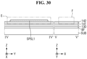
- FIG. 26 is a flowchart for illustrating an embodiment of S400 of FIG. 13 in detail.
- FIGS. 27 to 32 are enlarged cross-sectional views for illustrating S400 of FIG. 13 .
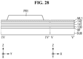
- the first metal layer ML1 is provided on an entirety of the second interlayer dielectric layer 142 (S410 of FIG. 26 ).
- the first metal layer ML1 may include or be made of a single layer or multiple layers among molybdenum (Mo), aluminum (Al), chromium (Cr), gold (Au), titanium (Ti), nickel (Ni), neodymium (Nd) and copper (Cu) and an alloy thereof.
- Mo molybdenum
- Al aluminum
- Cr chromium
- Au gold
- Ti titanium
- Ni nickel
- Nd neodymium
- Cu copper
- a first photoresist pattern PR1 is provided or formed on the first metal layer ML1 (S420 of FIG. 26 ).
- the first photoresist pattern PR1 may correspond to the first sub-power supply line SPSL1, the third sub-power supply line SPSL3 and the first sub-power supply pad line PSPL1.
- the first photoresist pattern PR1 may be provided or formed by providing a photoresist material on an entirety of the first metal layer ML1 and then exposing and developing the photoresist material using a mask.
- the photoresist material may be a photosensitive resin.
- the photoresist material may be either of a positive type, i.e., a portion exposed to light is removed by a developer, or of a negative type, e.g., a portion not exposed to light is removed by a developer.
- the portion of the first metal layer ML1 that is not covered by the first photoresist pattern PR1 is etched out, and the second interlayer dielectric layer 142 is partially etched (S430 of FIG. 26 ).
- the portion of the first metal layer ML1 that is not covered by the first photoresist pattern PR1 is etched out via a wet etching process or a dry etching process. In doing so, a portion of the second interlayer dielectric layer 142 that is exposed as the first metal layer ML1 is removed may be etched out to form stepped portions at an upper surface of the second interlayer dielectric layer 142.
- the first photoresist pattern PR1 is removed to complete the first sub-power supply line SPSL1 (S440 of FIG. 26 ).
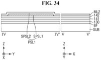
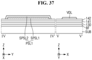
- FIG. 33 is a flowchart for illustrating an embodiment of S500 of FIG. 13 in detail.
- FIGS. 34 to 37 are enlarged cross-sectional views for illustrating S500 of FIG. 13 .
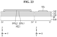
- a second metal layer ML2 is provided on an entirety of the second interlayer dielectric layer 142 and the first sub-power supply line SPSL1 (S510 of FIG. 33 ).
- the second metal layer ML2 may include or be made of a single layer or multiple layers among molybdenum (Mo), aluminum (Al), chromium (Cr), gold (Au), titanium (Ti), nickel (Ni), neodymium (Nd) and copper (Cu) and an alloy thereof.
- the second metal layer ML2 may include or be made of either the same material as or a different material from that of the first metal layer ML1.
- a second photoresist pattern PR2 is provided or formed on the second metal layer ML2 (S520 of FIG. 33 ).
- the second photoresist pattern PR2 may correspond to the driving voltage line VDL, the second sub-power supply line SPSL2, the fourth sub-power supply line SPSL4, the second sub-power supply pad line PSPL2, the first demux drain electrode MD1, the second demux drain electrode MD2 and the common source electrode MS.
- the second photoresist pattern PR2 may be provided or formed by providing a photoresist material on an entirety of the second metal layer ML2 and then exposing and developing the photoresist material using a mask.
- the portion of the second metal layer ML2 that is not covered by the second photoresist pattern PR2 is etched out such as by a wet etching process or a dry etching process. In doing so, a thickness portion of the second interlayer dielectric layer 142 that is exposed outside of the second photoresist pattern PR2 is removed as the second metal layer ML2 is etched out.
- the second photoresist pattern PR2 is removed to complete the second sub-power supply line SPSL2 and the driving voltage line VDL (S540 of FIG. 33 ).
- the portion of the second interlayer dielectric layer 142 overlapping the first sub-power supply line SPSL1 along the third direction (z-axis direction) is non-etched during the process of providing the first sub-power supply line SPSL1 ( FIGS. 29-31 ).
- the portion of the second interlayer dielectric layer 142 corresponding to the second sub-power supply line SPSL2 along the third direction (z-axis direction) is etched once ( FIGS. 29-31 ).
- the portion of the second interlayer dielectric layer 142 that does not overlap with either of the first sub-power supply line SPSL1 or the second sub-power supply line SPSL2 along the third direction (z-axis direction) is etched twice ( FIGS. 29-31 and FIG.
- the first thickness T1 of the second interlayer dielectric layer 142 corresponding to the first sub-power supply line SPSL1 along the third direction (z-axis direction) may be larger than the second thickness T2 of the second interlayer dielectric layer 142 corresponding to ends of the second sub-power supply line SPSL2 along the third direction (z-axis direction) ( FIG. 9 ).
- the second thickness T2 of the second interlayer dielectric layer 142 corresponding to the second sub-power supply line SPSL2 along the third direction (z-axis direction) may be larger than the third thickness T3 of the second interlayer dielectric layer 142 non-overlapping with both the first sub-power supply line SPSL1 and the second sub-power supply line SPSL2 along the third direction (z-axis direction) ( FIG. 9 ).
- the second thickness T2 of the second interlayer dielectric layer 142 overlapping with the driving voltage line VDL along the third direction (z-axis direction) may be smaller than the second thickness T2 of the second interlayer dielectric layer 142 overlapping with the second sub-power supply line SPSL2 along the third direction (z-axis direction) ( FIG. 9 ).
- a first power supply line PSL1 has a two-layer wiring structure including a first sub-power supply line SPSL1 and a second sub-power supply line SPSL2.
Landscapes
- Engineering & Computer Science (AREA)
- Microelectronics & Electronic Packaging (AREA)
- Manufacturing & Machinery (AREA)
- Devices For Indicating Variable Information By Combining Individual Elements (AREA)
- Electroluminescent Light Sources (AREA)
Claims (21)
- Dispositif d'affichage (10) comprenant :un substrat (SUB) comprenant une zone d'affichage (DA) et une zone de non-affichage (NDA) qui est adjacente à la zone d'affichage (DA) ;une première ligne d'alimentation électrique (PSL1) qui est dans la zone de non-affichage (NDA) et à travers laquelle une première tension d'alimentation est fournie à la zone d'affichage (DA) ; etune ligne de tension de pilotage qui est dans la zone d'affichage (DA) et connecte la première ligne d'alimentation électrique (PSL1) à la zone d'affichage (DA),caractérisé en ce quela première ligne d'alimentation électrique (PSL1) comprend :une première ligne d'alimentation électrique secondaire (SPSL1) dans la zone de non-affichage (NDA) ; etune deuxième ligne d'alimentation électrique secondaire (SPSL2) qui est dans la zone de non-affichage (NDA) et qui fait face à la première ligne d'alimentation électrique secondaire (SPSL1) suivant une direction d'épaisseur du substrat (SUB), la deuxième ligne d'alimentation électrique secondaire (SPSL2) s'étend le long d'un côté supérieur et de surfaces latérales de la première ligne d'alimentation électrique secondaire (SPSL1) et entrant en contact avec la première ligne d'alimentation électrique secondaire (SPSL1), etla deuxième ligne d'alimentation électrique secondaire (SPSL2) et la ligne de tension de pilotage (VDL) sont des motifs respectifs d'une même couche de matériau sur le substrat (SUB).
- Dispositif d'affichage (10) selon la revendication 1, dans lequel la deuxième ligne d'alimentation électrique secondaire (SPSL2) s'étend plus loin que la première ligne d'alimentation électrique secondaire (SPSL1) pour définir la ligne de tension de pilotage, et/ou dans lequel, au sein de la première ligne d'alimentation électrique (PSL1), la deuxième ligne d'alimentation électrique secondaire (SPSL2) entre en contact avec la première ligne d'alimentation électrique secondaire (SPSL1).
- Dispositif d'affichage (10) selon au moins l'une des revendications 1 ou 2, dans lequella ligne de tension de pilotage (VDL) s'étend à partir de la première ligne d'alimentation électrique (PSL1) suivant une première direction (x),chacune de la première ligne d'alimentation électrique secondaire (SPSL1) et de la deuxième ligne d'alimentation électrique secondaire (SPSL2) a une largeur suivant la première direction (x), etla largeur de la deuxième ligne d'alimentation électrique secondaire (SPSL2) est supérieure à la largeur de la première ligne d'alimentation électrique secondaire (SPSL1).
- Dispositif d'affichage (10) selon au moins l'une des revendications 1 à 3, comprenant en outre une couche isolante (142) entre le substrat et la première ligne d'alimentation électrique secondaire (SPSL1),
dans lequel la couche isolante (142) s'étend de la première ligne d'alimentation électrique secondaire (SPSL1) jusqu'à être entre le substrat (SUB) et la ligne de tension de pilotage (VDL). - Dispositif d'affichage (10) selon la revendication 4, dans lequel, suivant la direction d'épaisseur du substrat (SUB) :la couche isolante (142) a une épaisseur correspondant à la première ligne d'alimentation électrique secondaire (SPSL1) et une épaisseur correspondant à la ligne de tension de pilotage (VDL) de telle sorte que l'épaisseur (T1) de la couche isolante (142) dans une zone où la couche isolante (142) est en contact avec la première ligne d'alimentation électrique secondaire (SPSL1) est supérieure à l'épaisseur (T2) de la couche isolante (142) dans une zone où la couche isolante (142) est en contact avec la ligne de tension de pilotage (VDL), et/oudans lequel une différence entre les épaisseurs (T1) et (T2) va de 70 nm à 120 nm.
- Dispositif d'affichage (10) selon la revendication 5, dans lequella deuxième ligne d'alimentation électrique secondaire (SPSL2) s'étend plus loin que la première ligne d'alimentation électrique secondaire (SPSL1) pour définir une portion étendue de la deuxième ligne d'alimentation électrique secondaire (SPSL2), etsuivant la direction d'épaisseur du substrat (SUB) :
la couche isolante (142) a une épaisseur correspondant à la première ligne d'alimentation électrique secondaire (SPSL1) et une épaisseur correspondant à la portion étendue de la deuxième ligne d'alimentation électrique secondaire (SPSL2) de sorte que l'épaisseur (T1) de la couche isolante (142) dans une zone où la couche isolante (142) est en contact avec la première ligne d'alimentation électrique secondaire (SPSL1) est supérieure à l'épaisseur (T2) de la couche isolante (142) dans une zone où la couche isolante (142) est en contact avec la portion étendue de la deuxième ligne d'alimentation électrique secondaire (SPSL2). - Dispositif d'affichage (10) selon au moins l'une des revendications 1 à 6, comprenant en outre dans la zone de non-affichage :une pluralité de plots d'affichage (DP) à travers lesquels un signal électrique est fourni au dispositif d'affichage (10) depuis l'extérieur de celui-ci, la pluralité de plots d'affichage (DP) incluant un premier plot d'affichage (DP1) et un deuxième plot d'affichage (DP2) ;un pont d'alimentation électrique (PSB) connecté à la première ligne d'alimentation électrique (PSL1) ; etune première ligne de plot d'alimentation électrique (PSPL) qui connecte le premier plot d'affichage (DP) au pont d'alimentation électrique (PSB).
- Dispositif d'affichage (10) selon la revendication 7, comprenant en outre une couche de planarisation entre le pont d'alimentation électrique et la première ligne d'alimentation électrique et entre le pont d'alimentation électrique (PSB) et la première ligne de plot d'alimentation électrique et/ou comprenant un premier trou de contact de connexion d'alimentation (DCT1) qui est dans la couche de planarisation (160) et expose la deuxième ligne d'alimentation électrique secondaire (SPSL2) à l'extérieur de la couche de planarisation (160),
dans lequel le pont d'alimentation électrique (PSB) est connecté à la deuxième ligne d'alimentation électrique secondaire (SPSL2) par l'intermédiaire du premier trou de contact de connexion d'alimentation (DCT1) dans la couche de planarisation. - Dispositif d'affichage (10) selon la revendication 8, dans lequel la première ligne de plot d'alimentation électrique (PSPL) comprend :une première ligne de plot d'alimentation électrique secondaire (DSPL1) dans la zone de non-affichage (NDA) ; etune deuxième ligne de plot d'alimentation électrique secondaire (DSPL2) qui est dans la zone de non-affichage et fait face à la première ligne de plot d'alimentation électrique secondaire (DSPL1) suivant la direction d'épaisseur du substrat (SUB), etla deuxième ligne de plot d'alimentation électrique secondaire (DSPL2) et la ligne de tension de pilotage (VDL) sont des motifs respectifs d'une même couche de matériau sur le substrat.
- Dispositif d'affichage (10) selon la revendication 9, dans lequel au sein de la zone de non-affichage (NDA) :la première ligne d'alimentation électrique (PSL1), le pont d'alimentation électrique (PSB) et la première ligne de plot d'alimentation électrique (PSPL2) sont agencées suivant une première direction (x),chacune de la première ligne de plot d'alimentation électrique secondaire (PSPL1) et de la deuxième ligne de plot d'alimentation électrique secondaire (PSPL2) a une largeur suivant une deuxième direction (y) croisant la première direction (x), etla largeur de la deuxième ligne de plot d'alimentation électrique secondaire (PSPL2) est supérieure à la largeur de la première ligne de plot d'alimentation électrique secondaire (PSPL1), et/ou comprenant un deuxième trou de contact de connexion d'alimentation (DCT2) qui est dans la couche de planarisation et expose la deuxième ligne de plot d'alimentation électrique secondaire (PSPL2) à l'extérieur de la couche de planarisation,dans lequel le pont d'alimentation électrique (PSB) est connecté à la deuxième ligne de plot d'alimentation électrique secondaire (PSPL2) par l'intermédiaire du deuxième trou de contact de connexion d'alimentation (DCT2) dans la couche de planarisation.
- Dispositif d'affichage (10) selon au moins l'une des revendications 8 à 10, comprenant en outre un élément électroluminescent (LEL) dans la zone d'affichage, l'élément électroluminescent (LEL) comprenant une première électrode, une couche émissive et une deuxième électrode dans l'ordre à partir du substrat (SUB),
dans lequel le pont d'alimentation électrique (PSB) et la première électrode sont des motifs respectifs d'une même couche de matériau sur le substrat (SUB). - Dispositif d'affichage (10) selon au moins l'une des revendications 7 à 11, comprenant en outre :dans la zone d'affichage (DA), une pluralité de lignes de données (DL), et dans la zone de non-affichage (NDA), un transistor de démultiplexeur qui connecte le deuxième plot d'affichage (DP2) à la pluralité de lignes de données (DL),dans lequel le pont d'alimentation électrique (PSB) correspond au transistor de démultiplexeur (DMT) suivant la direction d'épaisseur du substrat (SUB).
- Dispositif d'affichage (10) selon la revendication 12, comprenant en outre :une électrode commune qui est dans la zone d'affichage (DA), etune deuxième ligne d'alimentation électrique (PSL2) qui est dans la zone de non-affichage (NDA) et à travers laquelle une deuxième tension d'alimentation différente de la première tension d'alimentation est fournie à l'électrode commune (173).
- Dispositif d'affichage (10) selon au moins l'une des revendications 1 à 13, comprenant :une couche isolante (142) qui est entre le substrat (SUB) et la première ligne d'alimentation électrique secondaire,dans lequella couche isolante (142) s'étend de la première ligne d'alimentation électrique secondaire (SPSL1) jusqu'à être entre le substrat (SUB) et la ligne de tension de pilotage (VDL), etsuivant la direction d'épaisseur du substrat (SUB) :
la couche isolante (142) a une épaisseur correspondant à la première ligne d'alimentation électrique secondaire (SPSL1) et une épaisseur correspondant à la ligne de tension de pilotage (VDL) de sorte que l'épaisseur (T1) de la couche isolante (142) dans une zone où la couche isolante (142) est en contact avec la première ligne d'alimentation électrique secondaire (SPSL1) est supérieure à l'épaisseur (T2) de la couche isolante (142) dans une zone où la couche isolante (142) est en contact avec la ligne de tension de pilotage (VDL). - Dispositif d'affichage (10) selon la revendication 14, dans lequel la deuxième ligne d'alimentation électrique secondaire (SPSL2) s'étend plus loin que la première ligne d'alimentation électrique secondaire (SPSL1) pour définir une portion étendue de la deuxième ligne d'alimentation électrique secondaire (SPSL2), et
suivant la direction d'épaisseur du substrat (SUB) :la couche isolante a une épaisseur correspondant à la première ligne d'alimentation électrique secondaire (SPSL1) et une épaisseur correspondant à la portion étendue de la deuxième ligne d'alimentation électrique secondaire (SPSL2), etl'épaisseur de la couche isolante qui correspond à la première ligne d'alimentation électrique secondaire (SPSL1) est supérieure à l'épaisseur de la couche isolante qui correspond à la portion étendue de la deuxième ligne d'alimentation électrique secondaire (SPSL2). - Dispositif d'affichage (10) selon au moins l'une des revendications 14 ou 15, dans lequel la deuxième ligne d'alimentation électrique secondaire et la ligne de tension de pilotage sont des motifs respectifs d'une même couche de matériau sur le substrat (SUB).
- Dispositif d'affichage (10) selon la revendication 16, dans lequel la première ligne d'alimentation électrique secondaire entre en contact avec la deuxième ligne d'alimentation électrique secondaire.
- Procédé de fourniture d'un dispositif d'affichage (10), le procédé comprenant :la fourniture dans une zone d'affichage (DA), d'un pixel (PX) comprenant un élément électroluminescent (LEL) sur un substrat (SUB) ;la fourniture dans une zone de non-affichage (NDA) qui est adjacente à la zone d'affichage (DA), d'une première couche de ligne d'alimentation électrique secondaire (SPSL1) d'une première ligne d'alimentation électrique (PSL1) à travers laquelle une tension d'alimentation est fournie à l'élément électroluminescent (LEL) ;la fourniture d'une couche isolante (142) entre le substrat et la première couche de ligne d'alimentation électrique secondaire (SPSL1) ; etla fourniture simultanée sur la couche isolante (142) à la fois :
d'une ligne de tension de pilotage (VDL) qui est dans la zone d'affichage et qui se connecte à la première ligne d'alimentation électrique (PSL1) au pixel, et d'une deuxième couche de ligne d'alimentation électrique secondaire (SPSL2) de la première ligne d'alimentation électrique (PSL1) qui est située dans une zone de la première couche de ligne d'alimentation électrique secondaire (SPSL1), dans lequel la deuxième couche de ligne d'alimentation électrique secondaire (SPSL2) s'étend le long d'un côté supérieur et de surfaces latérales de la première couche de ligne d'alimentation électrique secondaire (SPSL1) et entrant en contact avec la première ligne d'alimentation électrique secondaire (SPSL1). - Procédé selon la revendication 18, dans lequel la fourniture de la première couche de ligne d'alimentation électrique secondaire comprenant :la fourniture d'une première couche métallique sur la couche isolante ;la fourniture d'un premier motif de résine photosensible sur la première couche métallique ; etle retrait simultané d'une portion de la première couche métallique et d'une portion de la couche isolante qui sont exposées à l'extérieur du premier motif de résine photosensible.
- Procédé selon la revendication 19, dans lequel le retrait simultané de la portion de la première et/ou d'une deuxième couche métallique et de la portion de la couche isolante comprend le retrait de 70 nm à 120 nm de la couche isolante.
- Procédé selon au moins l'une des revendications 18 à 20, dans lequel la fourniture simultanée de la ligne de tension de pilotage et de la deuxième couche de ligne d'alimentation électrique secondaire comprend :la fourniture d'une deuxième couche métallique sur la couche isolante et la première couche de ligne d'alimentation électrique secondaire ;la fourniture d'un deuxième motif de résine photosensible sur la deuxième couche métallique ; etle retrait d'une portion de la deuxième couche métallique et d'une portion de la couche isolante qui sont exposées à l'extérieur du deuxième motif de résine photosensible.
Applications Claiming Priority (1)
| Application Number | Priority Date | Filing Date | Title |
|---|---|---|---|
| KR1020200100654A KR102872469B1 (ko) | 2020-08-11 | 2020-08-11 | 표시 장치와 그의 제조 방법 |
Publications (2)
| Publication Number | Publication Date |
|---|---|
| EP3961713A1 EP3961713A1 (fr) | 2022-03-02 |
| EP3961713B1 true EP3961713B1 (fr) | 2025-06-04 |
Family
ID=77168043
Family Applications (1)
| Application Number | Title | Priority Date | Filing Date |
|---|---|---|---|
| EP21188995.1A Active EP3961713B1 (fr) | 2020-08-11 | 2021-08-02 | Dispositif d'affichage et son procédé de fourniture |
Country Status (4)
| Country | Link |
|---|---|
| US (2) | US11950463B2 (fr) |
| EP (1) | EP3961713B1 (fr) |
| KR (1) | KR102872469B1 (fr) |
| CN (1) | CN114122005A (fr) |
Families Citing this family (5)
| Publication number | Priority date | Publication date | Assignee | Title |
|---|---|---|---|---|
| CN115623879A (zh) * | 2021-04-28 | 2023-01-17 | 京东方科技集团股份有限公司 | 显示基板、显示面板和显示基板制造方法 |
| CN115064108A (zh) * | 2022-06-30 | 2022-09-16 | 武汉天马微电子有限公司 | 显示面板及显示装置 |
| CN115498001B (zh) * | 2022-09-27 | 2026-04-10 | 武汉天马微电子有限公司 | 显示面板和显示装置 |
| CN119384890B (zh) * | 2023-05-25 | 2026-01-23 | 京东方科技集团股份有限公司 | 阵列基板和显示装置 |
| US20260164802A1 (en) * | 2024-06-21 | 2026-06-11 | Samsung Display Co., Ltd. | Display device and electronic device |
Family Cites Families (16)
| Publication number | Priority date | Publication date | Assignee | Title |
|---|---|---|---|---|
| US6284619B1 (en) * | 2000-06-29 | 2001-09-04 | International Business Machines Corporation | Integration scheme for multilevel metallization structures |
| KR100615212B1 (ko) | 2004-03-08 | 2006-08-25 | 삼성에스디아이 주식회사 | 평판 표시 장치 |
| KR101084256B1 (ko) * | 2009-12-08 | 2011-11-16 | 삼성모바일디스플레이주식회사 | 유기 발광 표시 장치 및 이의 제조 방법 |
| KR101188999B1 (ko) * | 2010-07-05 | 2012-10-08 | 삼성디스플레이 주식회사 | 유기 전계 발광 표시 장치 및 그 제조 방법 |
| KR101769586B1 (ko) | 2010-09-24 | 2017-08-21 | 삼성디스플레이 주식회사 | 유기 발광 디스플레이 장치 |
| TWI559064B (zh) * | 2012-10-19 | 2016-11-21 | 日本顯示器股份有限公司 | Display device |
| KR102460997B1 (ko) * | 2016-02-16 | 2022-11-01 | 삼성디스플레이 주식회사 | 표시 기판, 이의 제조 방법 및 이를 포함하는 표시 장치 |
| KR102562898B1 (ko) * | 2016-03-31 | 2023-08-04 | 삼성디스플레이 주식회사 | 표시 장치 |
| KR102328679B1 (ko) * | 2016-11-23 | 2021-11-19 | 삼성디스플레이 주식회사 | 표시 장치 |
| KR102594020B1 (ko) | 2016-12-07 | 2023-10-27 | 삼성디스플레이 주식회사 | 표시 장치 |
| KR102360353B1 (ko) * | 2017-07-28 | 2022-02-08 | 엘지디스플레이 주식회사 | 표시장치 |
| KR102427667B1 (ko) | 2017-09-26 | 2022-08-02 | 삼성디스플레이 주식회사 | 디스플레이 장치 |
| KR102612737B1 (ko) * | 2017-12-28 | 2023-12-12 | 엘지디스플레이 주식회사 | 표시장치 |
| KR102568920B1 (ko) * | 2018-06-29 | 2023-08-22 | 삼성디스플레이 주식회사 | 표시 장치 |
| KR20200028567A (ko) | 2018-09-06 | 2020-03-17 | 삼성디스플레이 주식회사 | 표시 장치 |
| KR102626223B1 (ko) | 2018-10-26 | 2024-01-17 | 삼성디스플레이 주식회사 | 표시 장치 |
-
2020
- 2020-08-11 KR KR1020200100654A patent/KR102872469B1/ko active Active
-
2021
- 2021-04-14 US US17/229,962 patent/US11950463B2/en active Active
- 2021-08-02 EP EP21188995.1A patent/EP3961713B1/fr active Active
- 2021-08-10 CN CN202110912908.XA patent/CN114122005A/zh active Pending
-
2024
- 2024-02-28 US US18/590,204 patent/US12329002B2/en active Active
Also Published As
| Publication number | Publication date |
|---|---|
| US20220052143A1 (en) | 2022-02-17 |
| EP3961713A1 (fr) | 2022-03-02 |
| KR20220020468A (ko) | 2022-02-21 |
| US11950463B2 (en) | 2024-04-02 |
| KR102872469B1 (ko) | 2025-10-17 |
| CN114122005A (zh) | 2022-03-01 |
| US12329002B2 (en) | 2025-06-10 |
| US20240260362A1 (en) | 2024-08-01 |
Similar Documents
| Publication | Publication Date | Title |
|---|---|---|
| US12329002B2 (en) | Sub-power lines in non-display area, display device including the same and method for providing the same | |
| US11387261B2 (en) | Array substrate and display device | |
| US12422966B2 (en) | Touch display panel, touch display apparatus and touch display mother board | |
| US20240188351A1 (en) | Stretchable display substrate, preparation method of stretchable display substrate, and display apparatus | |
| KR102892291B1 (ko) | 전계 발광 표시 장치 | |
| US20250351681A1 (en) | Display device and method of providing the same | |
| US12232367B2 (en) | Display device including swelling prevention layer | |
| KR20210097248A (ko) | 표시 장치 | |
| KR20210010696A (ko) | 표시 장치 | |
| US20250143079A1 (en) | Display device | |
| KR102839061B1 (ko) | 표시 장치와 그의 제조 방법 | |
| US8053981B2 (en) | Organic light-emitting device, and methods of forming the same and electronic devices having the same | |
| US20260033144A1 (en) | Display device and method for fabrication thereof | |
| US12501800B2 (en) | Display device | |
| CN119730596A (zh) | 显示装置 | |
| CN118900595A (zh) | 显示装置 | |
| JP4253181B2 (ja) | 画像表示パネル、フォトマスク、画像表示装置、画像表示パネルを製造する方法 | |
| EP4525592A1 (fr) | Dispositif d'affichage et son procédé de fabrication | |
| US20250160125A1 (en) | Display device and method of fabricating the same | |
| US20250089463A1 (en) | Display device and method of fabricating the same | |
| KR20250098054A (ko) | 표시 장치 및 그의 제조 방법 | |
| KR20250133027A (ko) | 표시 장치 | |
| CN120787065A (zh) | 显示装置 |
Legal Events
| Date | Code | Title | Description |
|---|---|---|---|
| PUAI | Public reference made under article 153(3) epc to a published international application that has entered the european phase |
Free format text: ORIGINAL CODE: 0009012 |
|
| STAA | Information on the status of an ep patent application or granted ep patent |
Free format text: STATUS: THE APPLICATION HAS BEEN PUBLISHED |
|
| AK | Designated contracting states |
Kind code of ref document: A1 Designated state(s): AL AT BE BG CH CY CZ DE DK EE ES FI FR GB GR HR HU IE IS IT LI LT LU LV MC MK MT NL NO PL PT RO RS SE SI SK SM TR |
|
| STAA | Information on the status of an ep patent application or granted ep patent |
Free format text: STATUS: REQUEST FOR EXAMINATION WAS MADE |
|
| 17P | Request for examination filed |
Effective date: 20220831 |
|
| RBV | Designated contracting states (corrected) |
Designated state(s): AL AT BE BG CH CY CZ DE DK EE ES FI FR GB GR HR HU IE IS IT LI LT LU LV MC MK MT NL NO PL PT RO RS SE SI SK SM TR |
|
| P01 | Opt-out of the competence of the unified patent court (upc) registered |
Effective date: 20230516 |
|
| STAA | Information on the status of an ep patent application or granted ep patent |
Free format text: STATUS: EXAMINATION IS IN PROGRESS |
|
| 17Q | First examination report despatched |
Effective date: 20230707 |
|
| REG | Reference to a national code |
Ref country code: DE Ref legal event code: R079 Free format text: PREVIOUS MAIN CLASS: H01L0027320000 Ipc: H10K0059131000 Ref country code: DE Ref legal event code: R079 Ref document number: 602021031643 Country of ref document: DE Free format text: PREVIOUS MAIN CLASS: H01L0027320000 Ipc: H10K0059131000 |
|
| RIC1 | Information provided on ipc code assigned before grant |
Ipc: H10K 59/131 20230101AFI20240819BHEP |
|
| GRAP | Despatch of communication of intention to grant a patent |
Free format text: ORIGINAL CODE: EPIDOSNIGR1 |
|
| STAA | Information on the status of an ep patent application or granted ep patent |
Free format text: STATUS: GRANT OF PATENT IS INTENDED |
|
| INTG | Intention to grant announced |
Effective date: 20241004 |
|
| GRAJ | Information related to disapproval of communication of intention to grant by the applicant or resumption of examination proceedings by the epo deleted |
Free format text: ORIGINAL CODE: EPIDOSDIGR1 |
|
| STAA | Information on the status of an ep patent application or granted ep patent |
Free format text: STATUS: EXAMINATION IS IN PROGRESS |
|
| GRAS | Grant fee paid |
Free format text: ORIGINAL CODE: EPIDOSNIGR3 |
|
| STAA | Information on the status of an ep patent application or granted ep patent |
Free format text: STATUS: GRANT OF PATENT IS INTENDED |
|
| GRAP | Despatch of communication of intention to grant a patent |
Free format text: ORIGINAL CODE: EPIDOSNIGR1 |
|
| INTC | Intention to grant announced (deleted) | ||
| INTG | Intention to grant announced |
Effective date: 20250217 |
|
| GRAA | (expected) grant |
Free format text: ORIGINAL CODE: 0009210 |
|
| STAA | Information on the status of an ep patent application or granted ep patent |
Free format text: STATUS: THE PATENT HAS BEEN GRANTED |
|
| AK | Designated contracting states |
Kind code of ref document: B1 Designated state(s): AL AT BE BG CH CY CZ DE DK EE ES FI FR GB GR HR HU IE IS IT LI LT LU LV MC MK MT NL NO PL PT RO RS SE SI SK SM TR |
|
| REG | Reference to a national code |
Ref country code: GB Ref legal event code: FG4D |
|
| REG | Reference to a national code |
Ref country code: CH Ref legal event code: EP |
|
| REG | Reference to a national code |
Ref country code: DE Ref legal event code: R096 Ref document number: 602021031643 Country of ref document: DE |
|
| REG | Reference to a national code |
Ref country code: IE Ref legal event code: FG4D |
|
| REG | Reference to a national code |
Ref country code: NL Ref legal event code: FP |
|
| PGFP | Annual fee paid to national office [announced via postgrant information from national office to epo] |
Ref country code: NL Payment date: 20250821 Year of fee payment: 5 |
|
| PG25 | Lapsed in a contracting state [announced via postgrant information from national office to epo] |
Ref country code: ES Free format text: LAPSE BECAUSE OF FAILURE TO SUBMIT A TRANSLATION OF THE DESCRIPTION OR TO PAY THE FEE WITHIN THE PRESCRIBED TIME-LIMIT Effective date: 20250604 Ref country code: FI Free format text: LAPSE BECAUSE OF FAILURE TO SUBMIT A TRANSLATION OF THE DESCRIPTION OR TO PAY THE FEE WITHIN THE PRESCRIBED TIME-LIMIT Effective date: 20250604 |
|
| PGFP | Annual fee paid to national office [announced via postgrant information from national office to epo] |
Ref country code: DE Payment date: 20250820 Year of fee payment: 5 |
|
| REG | Reference to a national code |
Ref country code: LT Ref legal event code: MG9D |
|
| PG25 | Lapsed in a contracting state [announced via postgrant information from national office to epo] |
Ref country code: GR Free format text: LAPSE BECAUSE OF FAILURE TO SUBMIT A TRANSLATION OF THE DESCRIPTION OR TO PAY THE FEE WITHIN THE PRESCRIBED TIME-LIMIT Effective date: 20250905 Ref country code: NO Free format text: LAPSE BECAUSE OF FAILURE TO SUBMIT A TRANSLATION OF THE DESCRIPTION OR TO PAY THE FEE WITHIN THE PRESCRIBED TIME-LIMIT Effective date: 20250904 |
|
| PG25 | Lapsed in a contracting state [announced via postgrant information from national office to epo] |
Ref country code: PL Free format text: LAPSE BECAUSE OF FAILURE TO SUBMIT A TRANSLATION OF THE DESCRIPTION OR TO PAY THE FEE WITHIN THE PRESCRIBED TIME-LIMIT Effective date: 20250604 |
|
| PG25 | Lapsed in a contracting state [announced via postgrant information from national office to epo] |
Ref country code: BG Free format text: LAPSE BECAUSE OF FAILURE TO SUBMIT A TRANSLATION OF THE DESCRIPTION OR TO PAY THE FEE WITHIN THE PRESCRIBED TIME-LIMIT Effective date: 20250604 |
|
| PGFP | Annual fee paid to national office [announced via postgrant information from national office to epo] |
Ref country code: GB Payment date: 20250820 Year of fee payment: 5 |
|
| PG25 | Lapsed in a contracting state [announced via postgrant information from national office to epo] |
Ref country code: HR Free format text: LAPSE BECAUSE OF FAILURE TO SUBMIT A TRANSLATION OF THE DESCRIPTION OR TO PAY THE FEE WITHIN THE PRESCRIBED TIME-LIMIT Effective date: 20250604 |
|
| PGFP | Annual fee paid to national office [announced via postgrant information from national office to epo] |
Ref country code: FR Payment date: 20250821 Year of fee payment: 5 Ref country code: AT Payment date: 20251020 Year of fee payment: 5 |
|
| PG25 | Lapsed in a contracting state [announced via postgrant information from national office to epo] |
Ref country code: RS Free format text: LAPSE BECAUSE OF FAILURE TO SUBMIT A TRANSLATION OF THE DESCRIPTION OR TO PAY THE FEE WITHIN THE PRESCRIBED TIME-LIMIT Effective date: 20250904 |
|
| PG25 | Lapsed in a contracting state [announced via postgrant information from national office to epo] |
Ref country code: LV Free format text: LAPSE BECAUSE OF FAILURE TO SUBMIT A TRANSLATION OF THE DESCRIPTION OR TO PAY THE FEE WITHIN THE PRESCRIBED TIME-LIMIT Effective date: 20250604 |
|
| PG25 | Lapsed in a contracting state [announced via postgrant information from national office to epo] |
Ref country code: PT Free format text: LAPSE BECAUSE OF FAILURE TO SUBMIT A TRANSLATION OF THE DESCRIPTION OR TO PAY THE FEE WITHIN THE PRESCRIBED TIME-LIMIT Effective date: 20251006 |
|
| REG | Reference to a national code |
Ref country code: AT Ref legal event code: MK05 Ref document number: 1801636 Country of ref document: AT Kind code of ref document: T Effective date: 20250604 |
|
| PG25 | Lapsed in a contracting state [announced via postgrant information from national office to epo] |
Ref country code: IS Free format text: LAPSE BECAUSE OF FAILURE TO SUBMIT A TRANSLATION OF THE DESCRIPTION OR TO PAY THE FEE WITHIN THE PRESCRIBED TIME-LIMIT Effective date: 20251004 |
|
| PG25 | Lapsed in a contracting state [announced via postgrant information from national office to epo] |
Ref country code: AT Free format text: LAPSE BECAUSE OF FAILURE TO SUBMIT A TRANSLATION OF THE DESCRIPTION OR TO PAY THE FEE WITHIN THE PRESCRIBED TIME-LIMIT Effective date: 20250604 Ref country code: SM Free format text: LAPSE BECAUSE OF FAILURE TO SUBMIT A TRANSLATION OF THE DESCRIPTION OR TO PAY THE FEE WITHIN THE PRESCRIBED TIME-LIMIT Effective date: 20250604 |
|
| PG25 | Lapsed in a contracting state [announced via postgrant information from national office to epo] |
Ref country code: CZ Free format text: LAPSE BECAUSE OF FAILURE TO SUBMIT A TRANSLATION OF THE DESCRIPTION OR TO PAY THE FEE WITHIN THE PRESCRIBED TIME-LIMIT Effective date: 20250604 |
|
| PG25 | Lapsed in a contracting state [announced via postgrant information from national office to epo] |
Ref country code: EE Free format text: LAPSE BECAUSE OF FAILURE TO SUBMIT A TRANSLATION OF THE DESCRIPTION OR TO PAY THE FEE WITHIN THE PRESCRIBED TIME-LIMIT Effective date: 20250604 |
|
| PG25 | Lapsed in a contracting state [announced via postgrant information from national office to epo] |
Ref country code: SK Free format text: LAPSE BECAUSE OF FAILURE TO SUBMIT A TRANSLATION OF THE DESCRIPTION OR TO PAY THE FEE WITHIN THE PRESCRIBED TIME-LIMIT Effective date: 20250604 Ref country code: RO Free format text: LAPSE BECAUSE OF FAILURE TO SUBMIT A TRANSLATION OF THE DESCRIPTION OR TO PAY THE FEE WITHIN THE PRESCRIBED TIME-LIMIT Effective date: 20250604 |
|
| PG25 | Lapsed in a contracting state [announced via postgrant information from national office to epo] |
Ref country code: IT Free format text: LAPSE BECAUSE OF FAILURE TO SUBMIT A TRANSLATION OF THE DESCRIPTION OR TO PAY THE FEE WITHIN THE PRESCRIBED TIME-LIMIT Effective date: 20250604 |
|
| REG | Reference to a national code |
Ref country code: DE Ref legal event code: R097 Ref document number: 602021031643 Country of ref document: DE |
|
| REG | Reference to a national code |
Ref country code: CH Ref legal event code: H13 Free format text: ST27 STATUS EVENT CODE: U-0-0-H10-H13 (AS PROVIDED BY THE NATIONAL OFFICE) Effective date: 20260324 |
|
| PG25 | Lapsed in a contracting state [announced via postgrant information from national office to epo] |
Ref country code: MC Free format text: LAPSE BECAUSE OF FAILURE TO SUBMIT A TRANSLATION OF THE DESCRIPTION OR TO PAY THE FEE WITHIN THE PRESCRIBED TIME-LIMIT Effective date: 20250604 |
|
| PLBE | No opposition filed within time limit |
Free format text: ORIGINAL CODE: 0009261 |
|
| STAA | Information on the status of an ep patent application or granted ep patent |
Free format text: STATUS: NO OPPOSITION FILED WITHIN TIME LIMIT |
|
| PG25 | Lapsed in a contracting state [announced via postgrant information from national office to epo] |
Ref country code: DK Free format text: LAPSE BECAUSE OF FAILURE TO SUBMIT A TRANSLATION OF THE DESCRIPTION OR TO PAY THE FEE WITHIN THE PRESCRIBED TIME-LIMIT Effective date: 20250604 |
|
| PG25 | Lapsed in a contracting state [announced via postgrant information from national office to epo] |
Ref country code: LU Free format text: LAPSE BECAUSE OF NON-PAYMENT OF DUE FEES Effective date: 20250802 |
|
| REG | Reference to a national code |
Ref country code: CH Ref legal event code: L10 Free format text: ST27 STATUS EVENT CODE: U-0-0-L10-L00 (AS PROVIDED BY THE NATIONAL OFFICE) Effective date: 20260416 |
|
| PG25 | Lapsed in a contracting state [announced via postgrant information from national office to epo] |
Ref country code: CH Free format text: LAPSE BECAUSE OF NON-PAYMENT OF DUE FEES Effective date: 20250831 |
|
| REG | Reference to a national code |
Ref country code: BE Ref legal event code: MM Effective date: 20250831 |
|
| 26N | No opposition filed |
Effective date: 20260305 |
|
| PG25 | Lapsed in a contracting state [announced via postgrant information from national office to epo] |
Ref country code: LT Free format text: LAPSE BECAUSE OF FAILURE TO SUBMIT A TRANSLATION OF THE DESCRIPTION OR TO PAY THE FEE WITHIN THE PRESCRIBED TIME-LIMIT Effective date: 20250604 |
|
| PG25 | Lapsed in a contracting state [announced via postgrant information from national office to epo] |
Ref country code: IE Free format text: LAPSE BECAUSE OF NON-PAYMENT OF DUE FEES Effective date: 20250802 Ref country code: BE Free format text: LAPSE BECAUSE OF NON-PAYMENT OF DUE FEES Effective date: 20250831 |
|
| PG25 | Lapsed in a contracting state [announced via postgrant information from national office to epo] |
Ref country code: SE Free format text: LAPSE BECAUSE OF FAILURE TO SUBMIT A TRANSLATION OF THE DESCRIPTION OR TO PAY THE FEE WITHIN THE PRESCRIBED TIME-LIMIT Effective date: 20250604 |