EP3961729B1 - Verfahren zur erzeugung einer germaniumstruktur und optische vorrichtung mit einer germaniumstruktur - Google Patents
Verfahren zur erzeugung einer germaniumstruktur und optische vorrichtung mit einer germaniumstruktur Download PDFInfo
- Publication number
- EP3961729B1 EP3961729B1 EP20193700.0A EP20193700A EP3961729B1 EP 3961729 B1 EP3961729 B1 EP 3961729B1 EP 20193700 A EP20193700 A EP 20193700A EP 3961729 B1 EP3961729 B1 EP 3961729B1
- Authority
- EP
- European Patent Office
- Prior art keywords
- germanium
- silicon substrate
- trench
- trenches
- germanium structure
- Prior art date
- Legal status (The legal status is an assumption and is not a legal conclusion. Google has not performed a legal analysis and makes no representation as to the accuracy of the status listed.)
- Active
Links
Images


Classifications
-
- H—ELECTRICITY
- H10—SEMICONDUCTOR DEVICES; ELECTRIC SOLID-STATE DEVICES NOT OTHERWISE PROVIDED FOR
- H10F—INORGANIC SEMICONDUCTOR DEVICES SENSITIVE TO INFRARED RADIATION, LIGHT, ELECTROMAGNETIC RADIATION OF SHORTER WAVELENGTH OR CORPUSCULAR RADIATION
- H10F71/00—Manufacture or treatment of devices covered by this subclass
- H10F71/121—The active layers comprising only Group IV materials
- H10F71/1212—The active layers comprising only Group IV materials consisting of germanium
-
- H—ELECTRICITY
- H10—SEMICONDUCTOR DEVICES; ELECTRIC SOLID-STATE DEVICES NOT OTHERWISE PROVIDED FOR
- H10F—INORGANIC SEMICONDUCTOR DEVICES SENSITIVE TO INFRARED RADIATION, LIGHT, ELECTROMAGNETIC RADIATION OF SHORTER WAVELENGTH OR CORPUSCULAR RADIATION
- H10F71/00—Manufacture or treatment of devices covered by this subclass
- H10F71/121—The active layers comprising only Group IV materials
-
- H—ELECTRICITY
- H10—SEMICONDUCTOR DEVICES; ELECTRIC SOLID-STATE DEVICES NOT OTHERWISE PROVIDED FOR
- H10F—INORGANIC SEMICONDUCTOR DEVICES SENSITIVE TO INFRARED RADIATION, LIGHT, ELECTROMAGNETIC RADIATION OF SHORTER WAVELENGTH OR CORPUSCULAR RADIATION
- H10F30/00—Individual radiation-sensitive semiconductor devices in which radiation controls the flow of current through the devices, e.g. photodetectors
- H10F30/20—Individual radiation-sensitive semiconductor devices in which radiation controls the flow of current through the devices, e.g. photodetectors the devices having potential barriers, e.g. phototransistors
- H10F30/21—Individual radiation-sensitive semiconductor devices in which radiation controls the flow of current through the devices, e.g. photodetectors the devices having potential barriers, e.g. phototransistors the devices being sensitive to infrared, visible or ultraviolet radiation
- H10F30/22—Individual radiation-sensitive semiconductor devices in which radiation controls the flow of current through the devices, e.g. photodetectors the devices having potential barriers, e.g. phototransistors the devices being sensitive to infrared, visible or ultraviolet radiation the devices having only one potential barrier, e.g. photodiodes
- H10F30/222—Individual radiation-sensitive semiconductor devices in which radiation controls the flow of current through the devices, e.g. photodetectors the devices having potential barriers, e.g. phototransistors the devices being sensitive to infrared, visible or ultraviolet radiation the devices having only one potential barrier, e.g. photodiodes the potential barrier being a PN heterojunction
-
- H—ELECTRICITY
- H10—SEMICONDUCTOR DEVICES; ELECTRIC SOLID-STATE DEVICES NOT OTHERWISE PROVIDED FOR
- H10F—INORGANIC SEMICONDUCTOR DEVICES SENSITIVE TO INFRARED RADIATION, LIGHT, ELECTROMAGNETIC RADIATION OF SHORTER WAVELENGTH OR CORPUSCULAR RADIATION
- H10F30/00—Individual radiation-sensitive semiconductor devices in which radiation controls the flow of current through the devices, e.g. photodetectors
- H10F30/20—Individual radiation-sensitive semiconductor devices in which radiation controls the flow of current through the devices, e.g. photodetectors the devices having potential barriers, e.g. phototransistors
- H10F30/21—Individual radiation-sensitive semiconductor devices in which radiation controls the flow of current through the devices, e.g. photodetectors the devices having potential barriers, e.g. phototransistors the devices being sensitive to infrared, visible or ultraviolet radiation
- H10F30/22—Individual radiation-sensitive semiconductor devices in which radiation controls the flow of current through the devices, e.g. photodetectors the devices having potential barriers, e.g. phototransistors the devices being sensitive to infrared, visible or ultraviolet radiation the devices having only one potential barrier, e.g. photodiodes
- H10F30/223—Individual radiation-sensitive semiconductor devices in which radiation controls the flow of current through the devices, e.g. photodetectors the devices having potential barriers, e.g. phototransistors the devices being sensitive to infrared, visible or ultraviolet radiation the devices having only one potential barrier, e.g. photodiodes the potential barrier being a PIN barrier
-
- H—ELECTRICITY
- H10—SEMICONDUCTOR DEVICES; ELECTRIC SOLID-STATE DEVICES NOT OTHERWISE PROVIDED FOR
- H10F—INORGANIC SEMICONDUCTOR DEVICES SENSITIVE TO INFRARED RADIATION, LIGHT, ELECTROMAGNETIC RADIATION OF SHORTER WAVELENGTH OR CORPUSCULAR RADIATION
- H10F77/00—Constructional details of devices covered by this subclass
- H10F77/10—Semiconductor bodies
- H10F77/12—Active materials
- H10F77/122—Active materials comprising only Group IV materials
-
- H—ELECTRICITY
- H10—SEMICONDUCTOR DEVICES; ELECTRIC SOLID-STATE DEVICES NOT OTHERWISE PROVIDED FOR
- H10F—INORGANIC SEMICONDUCTOR DEVICES SENSITIVE TO INFRARED RADIATION, LIGHT, ELECTROMAGNETIC RADIATION OF SHORTER WAVELENGTH OR CORPUSCULAR RADIATION
- H10F77/00—Constructional details of devices covered by this subclass
- H10F77/70—Surface textures, e.g. pyramid structures
- H10F77/703—Surface textures, e.g. pyramid structures of the semiconductor bodies, e.g. textured active layers
-
- H—ELECTRICITY
- H10—SEMICONDUCTOR DEVICES; ELECTRIC SOLID-STATE DEVICES NOT OTHERWISE PROVIDED FOR
- H10P—GENERIC PROCESSES OR APPARATUS FOR THE MANUFACTURE OR TREATMENT OF DEVICES COVERED BY CLASS H10
- H10P14/00—Formation of materials, e.g. in the shape of layers or pillars
- H10P14/20—Formation of materials, e.g. in the shape of layers or pillars of semiconductor materials
- H10P14/24—Formation of materials, e.g. in the shape of layers or pillars of semiconductor materials using chemical vapour deposition [CVD]
-
- H—ELECTRICITY
- H10—SEMICONDUCTOR DEVICES; ELECTRIC SOLID-STATE DEVICES NOT OTHERWISE PROVIDED FOR
- H10P—GENERIC PROCESSES OR APPARATUS FOR THE MANUFACTURE OR TREATMENT OF DEVICES COVERED BY CLASS H10
- H10P14/00—Formation of materials, e.g. in the shape of layers or pillars
- H10P14/20—Formation of materials, e.g. in the shape of layers or pillars of semiconductor materials
- H10P14/27—Formation of materials, e.g. in the shape of layers or pillars of semiconductor materials using selective deposition, e.g. simultaneous growth of monocrystalline and non-monocrystalline semiconductor materials
- H10P14/271—Formation of materials, e.g. in the shape of layers or pillars of semiconductor materials using selective deposition, e.g. simultaneous growth of monocrystalline and non-monocrystalline semiconductor materials characterised by the preparation of substrate for selective deposition
-
- H—ELECTRICITY
- H10—SEMICONDUCTOR DEVICES; ELECTRIC SOLID-STATE DEVICES NOT OTHERWISE PROVIDED FOR
- H10P—GENERIC PROCESSES OR APPARATUS FOR THE MANUFACTURE OR TREATMENT OF DEVICES COVERED BY CLASS H10
- H10P14/00—Formation of materials, e.g. in the shape of layers or pillars
- H10P14/20—Formation of materials, e.g. in the shape of layers or pillars of semiconductor materials
- H10P14/27—Formation of materials, e.g. in the shape of layers or pillars of semiconductor materials using selective deposition, e.g. simultaneous growth of monocrystalline and non-monocrystalline semiconductor materials
- H10P14/276—Lateral overgrowth
-
- H—ELECTRICITY
- H10—SEMICONDUCTOR DEVICES; ELECTRIC SOLID-STATE DEVICES NOT OTHERWISE PROVIDED FOR
- H10P—GENERIC PROCESSES OR APPARATUS FOR THE MANUFACTURE OR TREATMENT OF DEVICES COVERED BY CLASS H10
- H10P14/00—Formation of materials, e.g. in the shape of layers or pillars
- H10P14/20—Formation of materials, e.g. in the shape of layers or pillars of semiconductor materials
- H10P14/29—Formation of materials, e.g. in the shape of layers or pillars of semiconductor materials characterised by the substrates
- H10P14/2901—Materials
- H10P14/2902—Materials being Group IVA materials
- H10P14/2905—Silicon, silicon germanium or germanium
-
- H—ELECTRICITY
- H10—SEMICONDUCTOR DEVICES; ELECTRIC SOLID-STATE DEVICES NOT OTHERWISE PROVIDED FOR
- H10P—GENERIC PROCESSES OR APPARATUS FOR THE MANUFACTURE OR TREATMENT OF DEVICES COVERED BY CLASS H10
- H10P14/00—Formation of materials, e.g. in the shape of layers or pillars
- H10P14/20—Formation of materials, e.g. in the shape of layers or pillars of semiconductor materials
- H10P14/29—Formation of materials, e.g. in the shape of layers or pillars of semiconductor materials characterised by the substrates
- H10P14/2924—Structures
- H10P14/2925—Surface structures
-
- H—ELECTRICITY
- H10—SEMICONDUCTOR DEVICES; ELECTRIC SOLID-STATE DEVICES NOT OTHERWISE PROVIDED FOR
- H10P—GENERIC PROCESSES OR APPARATUS FOR THE MANUFACTURE OR TREATMENT OF DEVICES COVERED BY CLASS H10
- H10P14/00—Formation of materials, e.g. in the shape of layers or pillars
- H10P14/20—Formation of materials, e.g. in the shape of layers or pillars of semiconductor materials
- H10P14/29—Formation of materials, e.g. in the shape of layers or pillars of semiconductor materials characterised by the substrates
- H10P14/2926—Crystal orientations
-
- H—ELECTRICITY
- H10—SEMICONDUCTOR DEVICES; ELECTRIC SOLID-STATE DEVICES NOT OTHERWISE PROVIDED FOR
- H10P—GENERIC PROCESSES OR APPARATUS FOR THE MANUFACTURE OR TREATMENT OF DEVICES COVERED BY CLASS H10
- H10P14/00—Formation of materials, e.g. in the shape of layers or pillars
- H10P14/20—Formation of materials, e.g. in the shape of layers or pillars of semiconductor materials
- H10P14/34—Deposited materials, e.g. layers
- H10P14/3402—Deposited materials, e.g. layers characterised by the chemical composition
- H10P14/3404—Deposited materials, e.g. layers characterised by the chemical composition being Group IVA materials
- H10P14/3411—Silicon, silicon germanium or germanium
-
- H—ELECTRICITY
- H10—SEMICONDUCTOR DEVICES; ELECTRIC SOLID-STATE DEVICES NOT OTHERWISE PROVIDED FOR
- H10P—GENERIC PROCESSES OR APPARATUS FOR THE MANUFACTURE OR TREATMENT OF DEVICES COVERED BY CLASS H10
- H10P14/00—Formation of materials, e.g. in the shape of layers or pillars
- H10P14/20—Formation of materials, e.g. in the shape of layers or pillars of semiconductor materials
- H10P14/38—Formation of materials, e.g. in the shape of layers or pillars of semiconductor materials characterised by treatments done after the formation of the materials
-
- Y—GENERAL TAGGING OF NEW TECHNOLOGICAL DEVELOPMENTS; GENERAL TAGGING OF CROSS-SECTIONAL TECHNOLOGIES SPANNING OVER SEVERAL SECTIONS OF THE IPC; TECHNICAL SUBJECTS COVERED BY FORMER USPC CROSS-REFERENCE ART COLLECTIONS [XRACs] AND DIGESTS
- Y02—TECHNOLOGIES OR APPLICATIONS FOR MITIGATION OR ADAPTATION AGAINST CLIMATE CHANGE
- Y02P—CLIMATE CHANGE MITIGATION TECHNOLOGIES IN THE PRODUCTION OR PROCESSING OF GOODS
- Y02P70/00—Climate change mitigation technologies in the production process for final industrial or consumer products
- Y02P70/50—Manufacturing or production processes characterised by the final manufactured product
Definitions
- the present disclosure relates to methods for generating a germanium structure and, in particular, a germanium structure suitable to be used in an optical device. Furthermore, the present disclosure relates to optical devices comprising a germanium structure.
- Optical devices such as optical sensors or photovoltaic cells, are widely used.
- optical sensors such as miniaturized spectrometer or thermal imaging cameras, are increasingly applied in a plurality of fields, such as in consumer goods or in automotive applications.
- optical devices may convert the electromagnetic energy of light, such as visible or infrared light, into electricity, either to produce energy or to generate a sensor signal.
- Silicon is often used as semiconductor material for optical devices, such as optical detectors. Silicon is optically sensitive for light having a wavelength up to 1100 nm. There may be applications for optical devices which permit detection in a larger wavelength range exceeding the wavelength range detectable using silicon as the active material. In particular, in the field of food analytics, of medical technology and of material analytics interesting absorption bands of materials are in a wavelength range up to 1,8 ⁇ m.
- a material which is suitable for optical detectors due to its properties is germanium.
- NIR near infrared
- One of the challenges is to generate a germanium layer on a silicon layer with sufficient quality and within an acceptable time frame. Simply depositing a germanium layer onto a silicon layer may result in dislocations in the germanium layer due to different lattice constants of silicon and germanium, which may affect the electrical performance of the device. Since the costs of germanium exceed the costs of silicon many times using germanium as substrate material is generally not an option.
- trenches are etched in a layer, such as a silicon oxide layer, which is formed on a silicon layer.
- the trenches have a high aspect ratio, i.e. the height of the trenches is larger than the width of the trenches. Typically, the height may be three times the width.
- Germanium is grown up in the trench and beyond so that a germanium layer is formed on the silicon oxide layer. It is the object of the Aspect Ratio Trapping that dislocations in the germanium layer "outgrow" in the grown-up germanium layer at the side walls of the trench. Thereby, dislocations in the germanium trench decrease with increasing height.
- This technique is the basis for depositing pure thick layers of germanium, which are usable for optical applications.
- intermediate layers are used when depositing a germanium layer onto a silicon layer in order to reduce dislocations in the germanium layer.
- Such intermediate layers may be formed of Si x Ge y with different percentages of germanium from 1% to 100%. The percentage of silicon may be high in the first Si x Ge y layer deposited onto the silicon substrate and may decrease with increasing distance from the silicon substrate in order to realize a homogeneous transition. Thus, strain in the crystal structure at the transition between silicon and germanium may be reduced and less dislocations are generated which extend into the region of the germanium layer, which is to be functionalized.
- Such intermediate layers result in longer process times and a more complex processes.
- cyclic temperature processes are used to reduce dislocations in a transition between silicon and germanium.
- the temperature processes are performed at temperatures up to 900 °C with up to 10 repetitions. These process steps, which are in addition to the actual deposition of the germanium layer, are cost intensive and increase the complexity of the process. In addition, from a perspective point view, such high temperatures may not be compatible with a monolithic integration of the functional layers with standard CMOS processes.
- US 2007/099315 A1 A discloses a method of fabricating a germanium photo detector, wherein germanium is epitaxially grown in holes in a SiO 2 layer, followed by chemical mechanical polishing to remove most of the faceting region of the overgrown germanium chrystal. Thereafter, intrinsic germanium is grown on the epitaxially grown germanium and an etching step is provided to remove an outer peripheral region of the germanium.
- US 2011/049568 A1 discloses fabrication of monolithic lattice-mismatched semiconductor heterostructures, wherein Ge photodetectors may be integrated in a Si substrate by epitaxially growing GE material into apertures in an oxide layer formed on a Si substrate.
- US 2017/110334 A1 teaches epitaxially growing germanium material in trenches formed in a dielectric layer on a silicon substrate.
- One or more chemical and mechanical planarization processes are employed to planarize an overburden portion of the germanium material
- the present invention provides a method of generating an optical device according to claim 1 and an optical device according to claim 12. Futher developments of the invention are defined in the dependent claims.
- examples of the present disclosure provide a method of generating a germanium structure according to claim 1, which comprises performing an epitaxial depositing process on an assembly of a silicon substrate and an oxide layer, wherein one or more trenches in the oxide layer expose surface portions of the silicon substrate.
- the epitaxial depositing process comprises depositing germanium onto the assembly during a first phase, performing an etch process during a second phase following the first phase in order to remove germanium from the oxide layer, and repeating the first and second phases.
- a germanium crystal is grown up in the trench or each of a plurality of trenches.
- An optical device includes a light-incidence surface formed by a raw textured surface of a germanium structure obtained by an epitaxial depositing process without processing the surface of the germanium structure after the epitaxial process.
- a grown germanium structure is used as a basis for the production of optical devices, such as photo diodes, on a silicon semiconductor material.
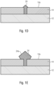
- an assembly 10 comprising a silicon substrate 12 and an oxide layer 14 is provided.
- the oxide layer 14 is provided on a surface 12a of the substrate 12 and comprises a trench 16.
- the trench 16 extends to the surface 12a of the substrate 12 so that a surface portion 20 of the substrate 12 is exposed.
- Oxide layer 14 may be a SiO layer.
- the depth d of the trench 16 is larger than the width w of the trench 16.
- the depth of the trench 16 is the dimension of the trench 16 in a vertical direction perpendicular to the substrate plane, wherein the substrate plane may be defined by the main surface 12a of the substrate, on which the oxide layer is provided.
- the width w of the trench is a (maximum) dimension of the trench between opposing side walls of the trench in a direction perpendicular to the vertical direction. In case the trench is circular when viewed in the vertical direction the width of the trench is the diameter of the trench. In case the trench is square-shaped when viewed in the vertical direction, the width of the trench corresponds to the side length of the square.
- the width is the distance between the two longer sides, while the distance between the two shorter sides is the length of the trench. In other words, in case of an elongate trench, the width of the trench is shorter than the length of the trench.
- the ratio between the trench depth and the trench width is at least two or at least three. In examples, the ratio between the trench depth and the trench width is three.
- the trench diameter or width, i.e. critical dimension, of the trench may be in the range from 100 nm to 2000 nm.
- the distance between trenches may be in the range from 500 nm to 5000 nm. In other examples, the distance between trenches is not critical.
- a germanium structure generated using a single trench may have a height in the range from 0,3 ⁇ m to 10 ⁇ m and a width/length of 0,3 ⁇ m to 9 ⁇ m.
- the dimensions may be correspondingly higher.
- providing assembly 10 may comprise forming trench 16 in the oxide layer.
- Forming trench 16 may include etching trench 16 into oxide layer 14. Thus, surface portion 20 is exposed.
- a plurality of corresponding trenches such as a row of at least two trenches or a two-dimensional array of at least four trenches, may be formed in the oxide layer.
- the preceding and following description with respect to one trench herein equally applies for each trench if the number of trenches is larger than one.
- the germanium crystal may be substantially monocrystalline with few dislocations, in particular in a region thereof distant from the silicon substrate on which it is grown.
- the epitaxial deposition process changes between depositing and etching the same material, i.e. germanium.
- the same material i.e. germanium.
- growth of polycrystalline grains on the surface of the wafer i.e. the oxide surface
- germanium structures as described herein are generated.
- the generated germanium structures may then be functionalized.
- germanium is deposited onto the top surface of the assembly 10 during a first phase and etching germanium is performed during a second phase.
- the first phase and the second phase take place one after the other and not concurrently.
- the first phase and the second phase are repeated multiple times in order to generate the germanium structure on the assembly 10.
- a duration of the first phase is longer than a duration of the second phase. In examples, the duration of the first phase is at least two times or at least three times the duration of the second phase.
- the germanium structure may be generated in a time efficient manner. In examples, the germanium structure may be formed within a time frame of 30 to 60 minutes.
- the epitaxial deposition process is performed at temperatures not exceeding 600°C.
- the temperature is controlled during the first and second phases to a temperature in a range of 300 C to 650°C, preferably in a range of 590°C to 610°C. In other examples, the temperature may be controlled to be in a range of 300°C to 400°C.
- examples permit performing the process at temperatures that permit a monolithic integration of the generated functional layers with standard CMOS processes.
- 1% GeH 4 in hydrogen may be used to achieve germanium deposition in the first phase.
- hydrochloric acid may be used for etching in the second phase.
- flow rates during the first and second phases are adapted to permit growing of the germanium crystal in a time-efficient manner.
- a flow rate of 1% GeH 4 in hydrogen is controlled during the first phases to be in a range of 350 sccm to 450 sccm, preferably in a range of 390 sccm to 410 sccm.
- a flow rate of hydrochloric acid is controlled during the second phases to be in a range of 40 sccm to 55 sccm, preferably in a range of 45 sccm to 49 sccm.
- the duration of the first phases may be in the order of 5s to 15s and the duration of the second phases may be in the order of 1s to 5s.
- the number of cycles, i.e. repetitions of the first phase and the second phase may be 100 or more.
- providing assembly 10 may comprise removing native SiO 2 from the ground of trench 16, i.e. from surface portion 20, before depositing germanium onto substrate portion 22 is started.
- removing native SiO 2 from the ground of trench 16 comprises baking the silicon substrate at a temperature in a range of 950°C to 1150°C, preferably in a range of 1040 °C to 1060°C, at a hydrogen flow in a range of 15 to 25 slm, preferably 19 to 21 slm, for a duration in a range of 120 to 240 s, preferably in a range of 145 s to 155 s.
- SiO 2 may be reduced to SiO, which is finally vaporized at the high temperature.
- removing native SiO 2 may comprise performing a wet etch process before the baking process The wet etch may take place at room temperature or at 35 °C, wherein the temperature at which the wet etch takes place is not critical). This wet etch process option allows to lower the temperature of the baking process to 850 °C. This permits removing the native SiO 2 at a reduced temperature when compared to the baking process without a wet etch.
- the germanium structure may be generated using the following parameters at a pressure of 133,3 hPa in both the first and second phases, which may be repeated 126 times.
- First phase duration 10s, 400 sccm of 1% GeH 4 in hydrogen, temperature 600°C.
- Second phase duration 3s, 47 sccm hydrochloric acid, temperature 600°C.
- a high temperature baking process at 1050°C at a hydrogen flow of 20slm for a duration of 150s may be performed prior to the epitaxial deposition process in order to remove native SiO 2 on the silicon surface on which the germanium structure is grown.
- Fig. 1B schematically shows the assembly 10 after a first phase, wherein a germanium crystal 24 is grown onto the ground of trench 16, i.e., on surface portion 20 of substrate 12.
- Fig. 1B schematically shows polycrystalline grains 22 formed on the surface 14a of the oxide layer 14.
- Fig. 1C shows the assembly 10 after a next second phase in which polycrystalline grains 22 are removed.
- Fig. 1D shows the assembly in a state in which the growing germanium crystal reached the top surface 14a of the oxide layer 14, such as after a number of repetitions of the first and second phases.
- the germanium crystal starts growing in the lateral direction in addition to growing in the vertical direction.
- the germanium crystal is formed in and on trench 16 and on regions of the oxide layer adjoining trench 16, such as regions of the oxide layer surrounding the trench 16.
- Fig. 1E shows the assembly after finishing the epitaxial deposition process.
- a bigger part of the germanium crystal may rest on the oxide layer surrounding the trench.
- the grown germanium crystal has a pyramid shape. This is the form of the germanium crystal as grown without any further processing thereof.
- Top surfaces 24a of the germanium crystal are arranged with an angle therebetween.
- the grown germanium crystal comprises a raw textured surface which may be used as a light incidence surface without any further processing of the germanium crystal.
- a pyramid shape of the germanium crystal is obtained when the germanium crystal is grown on a base material having a 100 orientation.
- base material having another orientation may be used and a germanium crystal having a raw textured surface with a different shape may be obtained by the epitaxial deposition process.
- the textured surface of the germanium structure obtained by the epitaxial depositing process is maintained and may be functionalized in order to be used as an active region of an optical device.
- the trenches may comprise a first trench and a second trench, wherein the germanium crystals formed on regions of the oxide layer adjoining the first and second trenches touch each other.
- the germanium crystals grown in the first and second trenches may grow together and may form a continuous germanium structure.
- a two-dimensional raster of trenches may be provided, wherein the germanium crystals associated with the trenches form a continuous germanium layer.
- a plurality of trenches may be provided with such a distance between adjacent trenches that germanium crystals grown in adjacent trenches grow together and form a continuous germanium structure.
- the distance between adjacent trenches may be adapted so that a raw textured surface, such as a surface comprising pyramid shaped projections, is formed by the epitaxial deposition process.
- a raw textured surface such as a surface comprising pyramid shaped projections
- larger germanium structures, such as layers, having a raw textured surface may be formed.
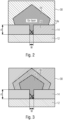
- Fig. 2 shows the germanium structure in the form of the grown crystal 24 on the assembly comprising the silicon substrate 12 and the silicon oxide 14. Inclined lines in trench 16 in Fig. 2 and other Figures are to indicate that dislocations in the grown-up germanium layer "outgrow" at the side walls of the trench.
- a protective layer is applied onto the germanium structure without conducting any planarization of the germanium structure before applying the protective layer.
- Fig. 2 shows a protective layer 30 formed on the top surface 14a of the oxide layer 14 and the germanium crystal 24.
- the protective layer may be an oxide layer, such as a silicon oxide layer. Examples comprise applying a protective layer onto the germanium structure without conducting any planarization of the germanium structure before applying the protective layer.
- the protective layer may provide a planar upper surface which may form the starting point for further processing, such as further processing to accomplish an optical device.
- a chemical mechanical polishing process may be performed with respect to the protective layer to achieve a planar upper surface of the protective layer.
- the germanium structure is functionalized, i.e. measures are taken that make the generated germanium structure suitable to be used as an active area in an optical device, such as a photodiode.
- the germanium structure is functionalized to be used as the active area to catch incident light and to convert the incident light into electric energy.
- at least parts of the silicon substrate and/or the germanium structure are doped so that a pn junction or a pin junction is formed by the silicon substrate and the germanium structure.
- dopants are added during and/or between at least a part of the first phases so as to generate doped regions of the germanium crystal.
- in-situ doping of a pn junction or a pin junction make take place between and/or during respective deposition phases.
- the doping may be introduced at a desired spatial position within the crystal.
- at least regions of the silicon substrate to which the number of trenches extend are doped. Regions of the silicon substrate to which different trenches of the number of trenches extend may be doped by the same doping type or different doping types.
- Fig. 3 shows an example of a generated germanium structure 24, wherein an upper portion 24b of the germanium structure represents an in-situ doped germanium layer.
- in-situ doping may take place during or after the last deposition phases of the epitaxial deposition process.
- the method according to the present invention comprises forming electrical connections to parts of the germanium structure and/or the silicon substrate so as to generate a sensor element capable of converting incident light into an electrical signal.
- the germanium structure may be functionalized to be used as an active area in an optical device.
- Examples of the present disclosure provide an optical device which may be formed using one of the methods described herein.
- the optical device comprises an epitaxially deposited germanium structure which is generated using one or more trenches in an oxide layer.
- the upper surface of the germanium structure is a raw textured surface which is directly formed by the deposition process and is used as a light incidence surface without further processing the germanium structure.
- the shape of the upper surface of the germanium structure is not changed after the deposition process but is used as it is as a light incidence surface of the optical device.
- a protective layer is formed over the silicon substrate and the germanium structure, the protective layer forming a planar surface facing away from the silicon substrate.
- the protective layer comprises silicon oxide.
- at least a portion of the silicon substrate adjoining the or each germanium crystal is doped with a first doping type, wherein at least a portion of the germanium structure is doped with a second doping type different from the first doping type, wherein a first electrical connection of the electrical connections is connected to the silicon substrate and a second electrical connection of the electrical connections is connected to the germanium structure.
- Examples of the optical device comprise at least a first trench and a second trench, wherein the germanium crystals formed on regions of the oxide layer adjoining the first and second trenches touch each other, wherein a first portion of the silicon substrate adjoining the germanium crystal in the first trench is doped with a first doping type, wherein a second portion of the silicon substrate adjoining the germanium crystal in the second trench is doped with a second doping type different from the first doping type, wherein a first electrical connection of the electrical connections is connected to the first portion of the silicon substrate and a second electrical connection of the electrical connections is connected to the second portion of the silicon substrate.
- the orientation of the surface of the silicon substrate on which the germanium structure is formed is ⁇ 100>, wherein the raw textured surface comprises a pyramid shape associated with each germanium crystal.
- Fig. 4 shows an example of an optical device based on the structure shown in Fig. 2 .
- a first electrical connection 40 is connected to the germanium structure 24 and a second electrical connection 42 is connected to silicon substrate 12.
- Electrical connections 40 and 42 may be formed by vias through oxide layers 14 and 30.
- Electrical connections 40 and 42 are further connected to conductive structures 44 and 46, which may connect connections 40 and 42 to a processing circuitry.
- conductive structures 44 and 46 may be part of a metallization layer of a CMOS structure including the processing circuitry.
- germanium structure 24 may be doped with a first doping type and silicon substrate 12 may be doped with a second doping type so that a pn junction is formed between germanium structure 24 and silicon substrate 12.
- the upper pyramid shaped surface of germanium structure 24 forms a light incidence surface of the optical device and germanium structure 24 forms an active area for converting incident light into electric energy.
- Fig. 5 shows an example of an optical device based on the structure shown in Fig. 3 .
- a first electrical connection 40 in form of a via connects germanium structure 24 to conductive structure 44 and a second electrical connection 42 connects silicon substrate 12 to conductive structure 46.
- Germanium structure 24 comprises an in-situ doped layer 24b, which is of the n type. The rest of germanium structure 24 is intrinsic. Silicon substrate 12 is of the p type. Thus, a pin junction is formed between germanium structure 24 and silicon substrate 12.
- the doping types may be changed and germanium layer 24b may be of the p type and silicon substrate 12 may be of the n type.
- the upper pyramid shaped surface of germanium structure 24 forms a light incidence surface of the optical device and the intrinsic part of the germanium structure 24 forms an active area for converting incident light into electric energy.
- Figures 6 and 7 show examples of optical devices in which the germanium structure is formed using two trenches 16a and 16b.
- a germanium crystal 54 grown using trench 16a and a germanium crystal 56 grown using trench 16b are grown together in the lateral direction to form a continuous germanium structure 24.
- an upper surface of germanium structure 24 comprises pyramid shaped protrusions, one associated with each germanium crystal 54 and 56.
- the upper surface is a textured surface forming a light incidence surface of the optical device.
- silicon substrate 12 is a p - substrate.
- a p + region 12a and a n + region 12b are formed in silicon substrate 12.
- p + region 12a is formed under trench 16a and n + region 12b is formed under trench 16b.
- Germanium structure 24 is of the intrinsic type.
- a first electrical connection 60 in form of a via connects p + region 12a to a conductive structure 44 and a second electrical connection 62 connects n + region 12b to a conductive structure 46.
- a pin junction is formed by regions 12a, 12b and germanium structure 24.
- silicon substrate 12 or at least portions of the silicon substrate under trenches 16a and 16b is or are of the p + type.
- Germaniums crystals 54 and 56 comprise respective n + doped germanium layers 54b and 56b, which may be in-situ doped as described above referring to Fig. 3 .
- a first electrical connection 60 connects silicon substrate 12 to a conductive structure 44 and a second electrical connection 64 connects germanium structure 24 to a conductive structure 46.
- a pin junction is formed by the p + silicon substrate 12, the intrinsic portions of the germanium structure and the n + doped germanium layers.
- the intrinsic parts of the germanium structure form an active area for converting incident light into electric energy.
- protection layer 30 may form a planar upper surface on which further circuit structures, such as wiring structures in the form of conductive structures 44 and 46 may be formed.
- Examples of the present disclosure permit the generation of high quality germanium structures using the Aspect Ratio Trapping (ART) technology on silicon substrates.
- Parts of the germanium structure at desired spatial positions may be in-situ doped during the generation of the germanium structure.
- the resulting shape of the germanium structure allows the conclusion that the germanium structure has a monocrystalline character with few dislocations in particular in a part thereof facing away from the silicon substrate.
- a protective layer such as formed of SiO, having a sufficient thickness to compensate for the uneven surface after the generation of the germanium structure may be applied.
- the protective layer may finally encase the grown germanium structure.
- a CMP (chemical mechanical polishing) process may be used to planarize the upper surface of the protective layer (without changing the shape of the grown germanium structure).
- Examples of the disclosure are based on the idea of using a germanium structure, such as a germanium layer or a layer consisting in part of germanium, which is grown onto a semiconductor substrate, such as a silicon substrate, directly as a structure for implementing an optical device, i.e. without further processing the germanium structure to amend the shape thereof.
- the grown germanium crystal may be used in the optical device in the form as it is originally grown.
- the upper surface of the generated germanium structure may have one or more pyramid shaped protrusions suitable to redirect incident light efficiently into the active area.
- germanium pyramids are utilized to fabricate devices directly in the germanium crystal with the possibility to monolithically integrate such devices with CMOS processes.
- a pn or pin junction may be generated in-situ during the deposition process, i.e., growing process.
- a thick oxide layer may be deposited as a protective layer to enclose and stabilize the germanium structure. Any topology on the upper surface of the protective layer may be planarized using a CMP process.
- Electrical connections to the germanium structure and/or the substrate may be implemented using standard materials and signals may be tapped via the substrate material or through the oxide layer on which most of the germanium structure rests. Conductive material may be applied as appropriate, such as on the oxide layer on which part of the germanium structure rests, prior to generating the germanium structure so as to directly connect the germanium structure to such conductive material.
- Examples of the present disclosure provide the possibility of a monolithic integration with other circuit structures, such as CMOS structures or an ASIC, application specific integrated circuit since the temperature at which the germanium is deposited may be compatible with those of CMOS or ASIC processes. In examples, the temperature at which the germanium structure is deposited may vary, wherein germanium deposition is possible at temperatures below 400°C.
- functionalized crystals and germanium structures may be combined individually or in groups, such as pixel, to obtain a sensor array, such as to implement a thermographic sensor.
- a sensor array such as to implement a thermographic sensor.
- the optical device according to the present disclosure may be used as an optical time of flight sensor, as an optical detector for LIDAR, light detection and ranging, as a spectrometer, as a multichannel spectrometer or as an optical detector for RF applications.
- Examples of the present disclosure permit optical devices usable for a large range of wavelengths since germanium offers an optical sensitivity up to 1,8 ⁇ m where absorption bands for different substances can be found, for example in food analysis, medical technology and material analysis. Thus, examples may improve optical applications, such as multichannel spectrometers or TOF sensors, which may profit substantially from the extended wavelength range.
Claims (15)
- Ein Verfahren zum Erzeugen einer optischen Vorrichtung, die eine Germaniumstruktur (24) aufweist, wobei das Verfahren folgende Schritte aufweist:Bereitstellen einer Anordnung (10), die ein Siliziumsubstrat (12) mit einer Oxidschicht (14) auf einer Oberfläche (12a) desselben aufweist, wobei die Oxidschicht (14) eine Anzahl von Gräben (16, 16a, 16b) aufweist, wobei sich jeder Graben (16, 16a, 16b) zu der Oberfläche (12a) des Siliziumsubstrats (12) erstreckt und einen Abschnitt (20) derselben freilegt, wobei eine Grabentiefe größer als eine Grabenbreite ist, wobei die Anzahl von Gräben (16, 16a, 16b) zumindest eins beträgt;Ausführen eines epitaktischen Aufbringungsprozesses an der Anordnung (10), um einen Germaniumkristall der Germaniumstruktur (24) an jedem freigelegten Abschnitt (20) des Siliziumsubstrats (12) aufzuwachsen, wobei jeder Germaniumkristall in dem zugeordneten Graben (16, 16a, 16b) und an Regionen der Oxidschicht (14), die an den zugeordneten Graben (16, 16a, 16b) angrenzen, gebildet ist, wobei der epitaktische Aufbringungsprozess folgende Schritte aufweist:Aufbringen von Germanium auf die Anordnung (10) während einer ersten Phase;Ausführen eines Ätzprozesses während einer zweiten, auf die erste Phase folgenden, Phase, um Germanium von der Oxidschicht (14) zu entfernen; undWiederholen der ersten und zweiten Phase;Ausbilden von elektrischen Verbindungen zu Teilen der Germaniumstruktur (24) und/oder des Siliziumsubstrats (12), um ein Sensorelement zu erzeugen, das einfallendes Licht in ein elektrisches Signal umwandeln kann,wobei zumindest Teile des Siliziumsubstrats (12) und/oder der Germaniumstruktur (24) dotiert sind, sodass ein pn-Übergang oder ein pin-Übergang durch das Siliziumsubstrat (12) und die Germaniumstruktur (24) gebildet wird,wobei die Germaniumstruktur (25) eine grobe, strukturierte Oberfläche aufweist, die ohne weitere Bearbeitung der Germaniumstruktur (24) eine Lichteinfallsfläche der optischen Vorrichtung bildet,wobei die Ausrichtung der Oberfläche des Siliziumsubstrats (12), auf der die Germaniumstruktur gebildet ist, <100> beträgt, wobei die grobe, strukturierte Oberfläche eine dem oder jedem Germaniumkristall zugeordnete Pyramidenform aufweist.
- Das Verfahren gemäß Anspruch 1, wobei eine Dauer der ersten Phase länger ist als eine Dauer der zweiten Phase, vorzugsweise zumindest doppelt oder zumindest dreimal so lang wie die Dauer der zweiten Phase.
- Das Verfahren gemäß einem der Ansprüche 1 und 2, das ein Steuern der Temperatur während der ersten und zweiten Phasen auf eine Temperatur in einem Bereich von 300 °C bis 650 °C, vorzugsweise in einem Bereich von 590 °C bis 610 °C, umfasst.
- Das Verfahren gemäß einem der Ansprüche 1 bis 3, das ein Steuern einer Flussrate von 1 % GeH4 in Wasserstoff während der ersten Phasen, sodass diese in einem Bereich von 350 sccm bis 450 sccm, vorzugsweise einem Bereich von 390 sccm bis 410 sccm, liegt, und ein Steuern einer Flussrate von Chlorwasserstoffsäure während der zweiten Phasen, sodass diese in einem Bereich von 40 sccm bis 55 sccm, vorzugsweise einem Bereich von 45 sccm bis 49 sccm, liegt, umfasst.
- Das Verfahren gemäß einem der Ansprüche 1 bis 4, das ein Entfernen von nativem SiO2 aus dem Grund von jedem Graben (16, 16a, 16b) aus der Anzahl von Gräben (16, 16a, 16b) vor erstmaliger Ausführung der ersten Phase umfasst.
- Das Verfahren gemäß Anspruch 5, bei dem das Entfernen von nativem SiO2 aus dem Grund von jedem Graben (16, 16a, 16b) folgende Schritte aufweist:a) Backen des Siliziumsubstrats (12) bei einer Temperatur in einem Bereich von 950 °C bis 1150 °C, vorzugsweise in einem Bereich von 1040 °C bis 1060 °C, bei einer Wasserstoff-Flussrate in einem Bereich von 15 bis 25 slm, vorzugsweise 19 bis 21 slm, über eine Dauer in einem Bereich von 120 bis 240 s, vorzugsweise in einem Bereich von 145 s bis 155 s, oderb) Ausführen eines Nassätzprozesses.
- Das Verfahren gemäß einem der Ansprüche 1 bis 6, bei dem die Anzahl von Gräben (16, 16a, 16b) zumindest einen ersten Graben (16a) und einen zweiten Graben (16b) aufweist, wobei die Germaniumkristalle, die an Regionen der Oxidschicht (14) ausgebildet sind, die an die ersten und zweiten Gräben (16a, 16b) angrenzen, einander berühren, und/oder wobei die Anzahl von Gräben ein zweidimensionales Raster von Gräben aufweist, wobei die den Gräben zugeordneten Germaniumkristalle eine durchgehende Germaniumschicht bilden.
- Das Verfahren gemäß einem der Ansprüche 1 bis 7, das ein Hinzufügen von Dotierungsstoffen während und/oder zwischen zumindest einem Teil der ersten Phasen umfasst, um dotierte Region des Germaniumkristalls zu erzeugen.
- Das Verfahren gemäß einem der Ansprüche 1 bis 8, bei dem zumindest Regionen des Siliziumsubstrats (12), zu denen sich die Anzahl von Gräben (16a, 16b) erstreckt, dotiert sind, wobei Regionen (12a, 12b) des Siliziumsubstrats (12), zu denen sich andere Gräben (16a, 16b) aus der Anzahl von Gräben (16a, 16b) erstrecken, mit demselben Dotierungsstoff-Typ oder unterschiedlichen Dotierungsstoff-Typen dotiert werden.
- Das Verfahren gemäß einem der Ansprüche 1 bis 9, bei dem die durch den epitaktischen Aufbringungsprozess strukturierte Oberfläche der Germaniumstruktur (24) erhalten wird.
- Das Verfahren gemäß einem der Ansprüche 1 bis 10, das ein Auftragen einer Schutzschicht, wie zum Beispiel Siliziumoxid, auf die Germaniumstruktur (24) umfasst, ohne dass jegliche Planarisierung der Germaniumstruktur (24) vor Auftragen der Schutzschicht durchgeführt wird.
- Eine optische Vorrichtung, die folgende Merkmale umfasst:ein Siliziumsubstrat (12);eine Oxidschicht (14) auf einer Oberfläche (12a) des Siliziumsubstrats (12), wobei die Oxidschicht (14) eine Anzahl von Gräben (16, 16a, 16b) aufweist, die sich zu der Oberfläche (12a) des Siliziumsubstrats (12) erstrecken, wobei eine Grabentiefe größer als eine Grabenbreite ist, wobei die Anzahl von Gräben (16, 16a, 16b) zumindest eins beträgt;eine epitaktisch aufgebrachte Germaniumstruktur (24) auf der Oberfläche (12a) des Siliziumsubstrats (12), wobei die Germaniumstruktur (24) einen Germaniumkristall in jedem aus der Anzahl von Gräben (16, 16a, 16b) und an Regionen der Oxidschicht (14), die an jeden Graben (16, 16a, 16b) angrenzen, aufweist;elektrische Verbindungen (40, 42, 60, 62, 64) zu Teilen der Germaniumstruktur (24) und/oder dem Siliziumsubstrat (12), wobei die Germaniumstruktur (24) zumindest Teil eines pn-Übergangs oder eines pin-Übergangs zwischen den elektrischen Verbindungen (40, 42, 60, 62, 64) bildet,eine Lichteinfallsfläche, die durch eine grobe, strukturierte Oberfläche der Germaniumstruktur (24) gebildet ist, die durch einen epitaktischen Aufbringungsprozess gewonnen wird, durch den die epitaktisch aufgebrachte Germaniumstruktur (24) ohne Bearbeiten der Oberfläche der Germaniumstruktur (24) nach dem epitaktischen Aufbringungsprozess erzeugt wird, wobei der epitaktische Aufbringungsprozess ein Aufbringen von Germanium auf die Anordnung (10) während einer ersten Phase, ein Ausführen eines Ätzprozesses während einer zweiten, auf die ersten Phase folgenden, Phase zum Entfernen von Germanium aus der Oxidschicht (14) und ein Wiederholen der ersten und zweiten Phasen umfasst,wobei die Ausrichtung der Oberfläche (12a) des Siliziumsubstrats (12), auf dem die Germaniumstruktur (24) gebildet ist, <100> beträgt, wobei die grobe, strukturierte Oberfläche eine dem oder jedem Germaniumkristall zugeordnete Pyramidenform aufweist.
- Die optische Vorrichtung gemäß Anspruch 12, die ferner eine Schutzschicht, wie zum Beispiel Siliziumoxid, aufweist, die über dem Siliziumsubstrat (12) und der Germaniumstruktur (24) ausgebildet ist, wobei die Schutzschicht eine planare von dem Siliziumsubstrat (12) abgewandte Oberfläche bildet.
- Die optische Vorrichtung gemäß einem der Ansprüche 12 und 13, bei der zumindest ein Teil (12a) des Siliziumsubstrats (12), der an den oder jeden Germaniumkristall angrenzt, mit einem ersten Dotierungsstoff-Typ dotiert ist, wobei zumindest ein Teil der Germaniumstruktur (24) mit einem zweiten Dotierungsstoff-Typ, der sich vom ersten Dotierungsstoff-Typ unterscheidet, dotiert ist, wobei eine erste elektrische Verbindung (42, 62) der elektrischen Verbindungen mit dem Siliziumsubstrat (12) verbunden ist und eine zweite elektrische Verbindung (40, 64) der elektrischen Verbindungen mit der Germaniumstruktur (24) verbunden ist.
- Die optische Vorrichtung gemäß einem der Ansprüche 12 bis 14, bei der die Anzahl von Gräben (16, 16a, 16b) zumindest einen ersten Graben (16a) und einen zweiten Graben (16b) aufweist, wobei die Germaniumkristalle, die an Regionen der Oxidschicht (14), die an die ersten und zweiten Gräben (16a, 16b) angrenzen, einander berühren, wobei ein erster Teil (12a) des Siliziumsubstrats (12), der an den Germaniumkristall im ersten Graben (16a) angrenzt, mit einem ersten Dotierungsstoff-Typ dotiert ist, wobei ein zweiter Teil (12b) des Siliziumsubstrats (12), der an den Germaniumkristall im zweiten Graben (16b) angrenzt, mit einem zweiten, vom ersten Dotierungsstoff-Typ unterschiedlichen, Dotierungsstoff-Typ dotiert ist, wobei eine erste elektrische Verbindung (60) der elektrischen Verbindungen mit dem ersten Teil (12a) des Siliziumsubstrats (12) verbunden ist und eine zweite elektrische Verbindung (62) der elektrischen Verbindungen mit dem zweiten Teil (12b) des Siliziumsubstrats (12) verbunden ist.
Priority Applications (4)
| Application Number | Priority Date | Filing Date | Title |
|---|---|---|---|
| EP20193700.0A EP3961729B1 (de) | 2020-08-31 | 2020-08-31 | Verfahren zur erzeugung einer germaniumstruktur und optische vorrichtung mit einer germaniumstruktur |
| KR1020210112301A KR102878646B1 (ko) | 2020-08-31 | 2021-08-25 | 게르마늄 구조체를 생성하는 방법과 게르마늄 구조체를 포함하는 광학 디바이스 |
| US17/461,159 US11594654B2 (en) | 2020-08-31 | 2021-08-30 | Method of generating a germanium structure and optical device comprising a germanium structure |
| CN202111004847.3A CN114121603A (zh) | 2020-08-31 | 2021-08-30 | 生成锗结构的方法和包括锗结构的光学器件 |
Applications Claiming Priority (1)
| Application Number | Priority Date | Filing Date | Title |
|---|---|---|---|
| EP20193700.0A EP3961729B1 (de) | 2020-08-31 | 2020-08-31 | Verfahren zur erzeugung einer germaniumstruktur und optische vorrichtung mit einer germaniumstruktur |
Publications (2)
| Publication Number | Publication Date |
|---|---|
| EP3961729A1 EP3961729A1 (de) | 2022-03-02 |
| EP3961729B1 true EP3961729B1 (de) | 2023-10-18 |
Family
ID=72292427
Family Applications (1)
| Application Number | Title | Priority Date | Filing Date |
|---|---|---|---|
| EP20193700.0A Active EP3961729B1 (de) | 2020-08-31 | 2020-08-31 | Verfahren zur erzeugung einer germaniumstruktur und optische vorrichtung mit einer germaniumstruktur |
Country Status (4)
| Country | Link |
|---|---|
| US (1) | US11594654B2 (de) |
| EP (1) | EP3961729B1 (de) |
| KR (1) | KR102878646B1 (de) |
| CN (1) | CN114121603A (de) |
Family Cites Families (4)
| Publication number | Priority date | Publication date | Assignee | Title |
|---|---|---|---|---|
| US8324660B2 (en) * | 2005-05-17 | 2012-12-04 | Taiwan Semiconductor Manufacturing Company, Ltd. | Lattice-mismatched semiconductor structures with reduced dislocation defect densities and related methods for device fabrication |
| US7358107B2 (en) * | 2005-10-27 | 2008-04-15 | Sharp Laboratories Of America, Inc. | Method of fabricating a germanium photo detector on a high quality germanium epitaxial overgrowth layer |
| KR101750742B1 (ko) * | 2011-10-14 | 2017-06-28 | 삼성전자주식회사 | 광검출기 구조체 |
| US9646842B1 (en) * | 2015-10-14 | 2017-05-09 | International Business Machines Corporation | Germanium smoothing and chemical mechanical planarization processes |
-
2020
- 2020-08-31 EP EP20193700.0A patent/EP3961729B1/de active Active
-
2021
- 2021-08-25 KR KR1020210112301A patent/KR102878646B1/ko active Active
- 2021-08-30 CN CN202111004847.3A patent/CN114121603A/zh active Pending
- 2021-08-30 US US17/461,159 patent/US11594654B2/en active Active
Also Published As
| Publication number | Publication date |
|---|---|
| CN114121603A (zh) | 2022-03-01 |
| US11594654B2 (en) | 2023-02-28 |
| KR20220030174A (ko) | 2022-03-10 |
| EP3961729A1 (de) | 2022-03-02 |
| US20220069156A1 (en) | 2022-03-03 |
| KR102878646B1 (ko) | 2025-11-03 |
Similar Documents
| Publication | Publication Date | Title |
|---|---|---|
| US11703643B2 (en) | Integrated photonics including waveguiding material | |
| CN102034833B (zh) | 传感器及其制造方法 | |
| US11127875B2 (en) | Method for manufacturing at least one passivated planar photodiode with reduced dark current | |
| US12166063B2 (en) | Optoelectronic device having an array of germanium-based diodes with low dark current | |
| US12382732B2 (en) | Passivated photodiode comprising a ferroelectric peripheral portion | |
| WO2010005772A2 (en) | Germanium diode | |
| US11508870B2 (en) | Process for fabricating at least one tensilely strained planar photodiode | |
| US20210111205A1 (en) | Optoelectronic device having a diode put under tensile stress by an inverse piezoelectric effect | |
| US9899441B1 (en) | Deep trench isolation (DTI) structure with a tri-layer passivation layer | |
| WO2022146822A1 (en) | Methods for forming image sensors | |
| KR20150130829A (ko) | 수평형 포토 다이오드, 이를 포함하는 이미지 센서 및 포토 다이오드, 이미지센서의 제조방법 | |
| EP3707755B1 (de) | Germanium auf isolator für cmos-bildgeber im kurzwelligen infrarot | |
| US9246045B2 (en) | Method for fabricating a photodetector | |
| EP3961729B1 (de) | Verfahren zur erzeugung einer germaniumstruktur und optische vorrichtung mit einer germaniumstruktur | |
| US12015097B2 (en) | Germanium-based planar photodiode with a compressed lateral peripheral zone | |
| WO2009146264A1 (en) | Method for electronically pinning a back surface of a back-illuminated imager fabricated on a utsoi wafer | |
| Vu et al. | PIN germanium photodetector fabrication issues and manufacturability | |
| CN118198188B (zh) | 一种半导体器件及其制备方法 | |
| JP2005534186A (ja) | 放射線硬化された可視p−i−n型検出器 | |
| US20090065819A1 (en) | Apparatus and method of manufacture for an imager starting material | |
| EP4673978A1 (de) | Photodetektor und verfahren zu seiner herstellung |
Legal Events
| Date | Code | Title | Description |
|---|---|---|---|
| PUAI | Public reference made under article 153(3) epc to a published international application that has entered the european phase |
Free format text: ORIGINAL CODE: 0009012 |
|
| STAA | Information on the status of an ep patent application or granted ep patent |
Free format text: STATUS: REQUEST FOR EXAMINATION WAS MADE |
|
| 17P | Request for examination filed |
Effective date: 20210921 |
|
| AK | Designated contracting states |
Kind code of ref document: A1 Designated state(s): AL AT BE BG CH CY CZ DE DK EE ES FI FR GB GR HR HU IE IS IT LI LT LU LV MC MK MT NL NO PL PT RO RS SE SI SK SM TR |
|
| STAA | Information on the status of an ep patent application or granted ep patent |
Free format text: STATUS: EXAMINATION IS IN PROGRESS |
|
| 17Q | First examination report despatched |
Effective date: 20221004 |
|
| REG | Reference to a national code |
Ref country code: DE Ref legal event code: R079 Free format text: PREVIOUS MAIN CLASS: H01L0031180000 Ipc: H01L0031109000 Ref country code: DE Ref legal event code: R079 Ref document number: 602020019359 Country of ref document: DE Free format text: PREVIOUS MAIN CLASS: H01L0031180000 Ipc: H01L0031109000 |
|
| RIC1 | Information provided on ipc code assigned before grant |
Ipc: H01L 21/02 20060101ALI20230321BHEP Ipc: H01L 31/18 20060101ALI20230321BHEP Ipc: H01L 31/105 20060101ALI20230321BHEP Ipc: H01L 31/109 20060101AFI20230321BHEP |
|
| GRAP | Despatch of communication of intention to grant a patent |
Free format text: ORIGINAL CODE: EPIDOSNIGR1 |
|
| STAA | Information on the status of an ep patent application or granted ep patent |
Free format text: STATUS: GRANT OF PATENT IS INTENDED |
|
| INTG | Intention to grant announced |
Effective date: 20230508 |
|
| P01 | Opt-out of the competence of the unified patent court (upc) registered |
Effective date: 20230630 |
|
| GRAS | Grant fee paid |
Free format text: ORIGINAL CODE: EPIDOSNIGR3 |
|
| GRAA | (expected) grant |
Free format text: ORIGINAL CODE: 0009210 |
|
| STAA | Information on the status of an ep patent application or granted ep patent |
Free format text: STATUS: THE PATENT HAS BEEN GRANTED |
|
| AK | Designated contracting states |
Kind code of ref document: B1 Designated state(s): AL AT BE BG CH CY CZ DE DK EE ES FI FR GB GR HR HU IE IS IT LI LT LU LV MC MK MT NL NO PL PT RO RS SE SI SK SM TR |
|
| REG | Reference to a national code |
Ref country code: GB Ref legal event code: FG4D |
|
| REG | Reference to a national code |
Ref country code: CH Ref legal event code: EP |
|
| REG | Reference to a national code |
Ref country code: IE Ref legal event code: FG4D |
|
| REG | Reference to a national code |
Ref country code: DE Ref legal event code: R096 Ref document number: 602020019359 Country of ref document: DE |
|
| REG | Reference to a national code |
Ref country code: LT Ref legal event code: MG9D |
|
| REG | Reference to a national code |
Ref country code: NL Ref legal event code: MP Effective date: 20231018 |
|
| REG | Reference to a national code |
Ref country code: AT Ref legal event code: MK05 Ref document number: 1623249 Country of ref document: AT Kind code of ref document: T Effective date: 20231018 |
|
| PG25 | Lapsed in a contracting state [announced via postgrant information from national office to epo] |
Ref country code: NL Free format text: LAPSE BECAUSE OF FAILURE TO SUBMIT A TRANSLATION OF THE DESCRIPTION OR TO PAY THE FEE WITHIN THE PRESCRIBED TIME-LIMIT Effective date: 20231018 |
|
| PG25 | Lapsed in a contracting state [announced via postgrant information from national office to epo] |
Ref country code: GR Free format text: LAPSE BECAUSE OF FAILURE TO SUBMIT A TRANSLATION OF THE DESCRIPTION OR TO PAY THE FEE WITHIN THE PRESCRIBED TIME-LIMIT Effective date: 20240119 |
|
| PG25 | Lapsed in a contracting state [announced via postgrant information from national office to epo] |
Ref country code: IS Free format text: LAPSE BECAUSE OF FAILURE TO SUBMIT A TRANSLATION OF THE DESCRIPTION OR TO PAY THE FEE WITHIN THE PRESCRIBED TIME-LIMIT Effective date: 20240218 |
|
| PG25 | Lapsed in a contracting state [announced via postgrant information from national office to epo] |
Ref country code: LT Free format text: LAPSE BECAUSE OF FAILURE TO SUBMIT A TRANSLATION OF THE DESCRIPTION OR TO PAY THE FEE WITHIN THE PRESCRIBED TIME-LIMIT Effective date: 20231018 |
|
| PG25 | Lapsed in a contracting state [announced via postgrant information from national office to epo] |
Ref country code: AT Free format text: LAPSE BECAUSE OF FAILURE TO SUBMIT A TRANSLATION OF THE DESCRIPTION OR TO PAY THE FEE WITHIN THE PRESCRIBED TIME-LIMIT Effective date: 20231018 |
|
| PG25 | Lapsed in a contracting state [announced via postgrant information from national office to epo] |
Ref country code: ES Free format text: LAPSE BECAUSE OF FAILURE TO SUBMIT A TRANSLATION OF THE DESCRIPTION OR TO PAY THE FEE WITHIN THE PRESCRIBED TIME-LIMIT Effective date: 20231018 |
|
| PG25 | Lapsed in a contracting state [announced via postgrant information from national office to epo] |
Ref country code: LT Free format text: LAPSE BECAUSE OF FAILURE TO SUBMIT A TRANSLATION OF THE DESCRIPTION OR TO PAY THE FEE WITHIN THE PRESCRIBED TIME-LIMIT Effective date: 20231018 Ref country code: IS Free format text: LAPSE BECAUSE OF FAILURE TO SUBMIT A TRANSLATION OF THE DESCRIPTION OR TO PAY THE FEE WITHIN THE PRESCRIBED TIME-LIMIT Effective date: 20240218 Ref country code: GR Free format text: LAPSE BECAUSE OF FAILURE TO SUBMIT A TRANSLATION OF THE DESCRIPTION OR TO PAY THE FEE WITHIN THE PRESCRIBED TIME-LIMIT Effective date: 20240119 Ref country code: ES Free format text: LAPSE BECAUSE OF FAILURE TO SUBMIT A TRANSLATION OF THE DESCRIPTION OR TO PAY THE FEE WITHIN THE PRESCRIBED TIME-LIMIT Effective date: 20231018 Ref country code: BG Free format text: LAPSE BECAUSE OF FAILURE TO SUBMIT A TRANSLATION OF THE DESCRIPTION OR TO PAY THE FEE WITHIN THE PRESCRIBED TIME-LIMIT Effective date: 20240118 Ref country code: AT Free format text: LAPSE BECAUSE OF FAILURE TO SUBMIT A TRANSLATION OF THE DESCRIPTION OR TO PAY THE FEE WITHIN THE PRESCRIBED TIME-LIMIT Effective date: 20231018 Ref country code: PT Free format text: LAPSE BECAUSE OF FAILURE TO SUBMIT A TRANSLATION OF THE DESCRIPTION OR TO PAY THE FEE WITHIN THE PRESCRIBED TIME-LIMIT Effective date: 20240219 |
|
| PG25 | Lapsed in a contracting state [announced via postgrant information from national office to epo] |
Ref country code: SE Free format text: LAPSE BECAUSE OF FAILURE TO SUBMIT A TRANSLATION OF THE DESCRIPTION OR TO PAY THE FEE WITHIN THE PRESCRIBED TIME-LIMIT Effective date: 20231018 Ref country code: RS Free format text: LAPSE BECAUSE OF FAILURE TO SUBMIT A TRANSLATION OF THE DESCRIPTION OR TO PAY THE FEE WITHIN THE PRESCRIBED TIME-LIMIT Effective date: 20231018 Ref country code: PL Free format text: LAPSE BECAUSE OF FAILURE TO SUBMIT A TRANSLATION OF THE DESCRIPTION OR TO PAY THE FEE WITHIN THE PRESCRIBED TIME-LIMIT Effective date: 20231018 Ref country code: NO Free format text: LAPSE BECAUSE OF FAILURE TO SUBMIT A TRANSLATION OF THE DESCRIPTION OR TO PAY THE FEE WITHIN THE PRESCRIBED TIME-LIMIT Effective date: 20240118 Ref country code: LV Free format text: LAPSE BECAUSE OF FAILURE TO SUBMIT A TRANSLATION OF THE DESCRIPTION OR TO PAY THE FEE WITHIN THE PRESCRIBED TIME-LIMIT Effective date: 20231018 Ref country code: HR Free format text: LAPSE BECAUSE OF FAILURE TO SUBMIT A TRANSLATION OF THE DESCRIPTION OR TO PAY THE FEE WITHIN THE PRESCRIBED TIME-LIMIT Effective date: 20231018 |
|
| PG25 | Lapsed in a contracting state [announced via postgrant information from national office to epo] |
Ref country code: DK Free format text: LAPSE BECAUSE OF FAILURE TO SUBMIT A TRANSLATION OF THE DESCRIPTION OR TO PAY THE FEE WITHIN THE PRESCRIBED TIME-LIMIT Effective date: 20231018 |
|
| REG | Reference to a national code |
Ref country code: DE Ref legal event code: R097 Ref document number: 602020019359 Country of ref document: DE |
|
| PG25 | Lapsed in a contracting state [announced via postgrant information from national office to epo] |
Ref country code: CZ Free format text: LAPSE BECAUSE OF FAILURE TO SUBMIT A TRANSLATION OF THE DESCRIPTION OR TO PAY THE FEE WITHIN THE PRESCRIBED TIME-LIMIT Effective date: 20231018 |
|
| PG25 | Lapsed in a contracting state [announced via postgrant information from national office to epo] |
Ref country code: SK Free format text: LAPSE BECAUSE OF FAILURE TO SUBMIT A TRANSLATION OF THE DESCRIPTION OR TO PAY THE FEE WITHIN THE PRESCRIBED TIME-LIMIT Effective date: 20231018 |
|
| PG25 | Lapsed in a contracting state [announced via postgrant information from national office to epo] |
Ref country code: SM Free format text: LAPSE BECAUSE OF FAILURE TO SUBMIT A TRANSLATION OF THE DESCRIPTION OR TO PAY THE FEE WITHIN THE PRESCRIBED TIME-LIMIT Effective date: 20231018 Ref country code: SK Free format text: LAPSE BECAUSE OF FAILURE TO SUBMIT A TRANSLATION OF THE DESCRIPTION OR TO PAY THE FEE WITHIN THE PRESCRIBED TIME-LIMIT Effective date: 20231018 Ref country code: RO Free format text: LAPSE BECAUSE OF FAILURE TO SUBMIT A TRANSLATION OF THE DESCRIPTION OR TO PAY THE FEE WITHIN THE PRESCRIBED TIME-LIMIT Effective date: 20231018 Ref country code: IT Free format text: LAPSE BECAUSE OF FAILURE TO SUBMIT A TRANSLATION OF THE DESCRIPTION OR TO PAY THE FEE WITHIN THE PRESCRIBED TIME-LIMIT Effective date: 20231018 Ref country code: EE Free format text: LAPSE BECAUSE OF FAILURE TO SUBMIT A TRANSLATION OF THE DESCRIPTION OR TO PAY THE FEE WITHIN THE PRESCRIBED TIME-LIMIT Effective date: 20231018 Ref country code: DK Free format text: LAPSE BECAUSE OF FAILURE TO SUBMIT A TRANSLATION OF THE DESCRIPTION OR TO PAY THE FEE WITHIN THE PRESCRIBED TIME-LIMIT Effective date: 20231018 Ref country code: CZ Free format text: LAPSE BECAUSE OF FAILURE TO SUBMIT A TRANSLATION OF THE DESCRIPTION OR TO PAY THE FEE WITHIN THE PRESCRIBED TIME-LIMIT Effective date: 20231018 |
|
| PLBE | No opposition filed within time limit |
Free format text: ORIGINAL CODE: 0009261 |
|
| STAA | Information on the status of an ep patent application or granted ep patent |
Free format text: STATUS: NO OPPOSITION FILED WITHIN TIME LIMIT |
|
| 26N | No opposition filed |
Effective date: 20240719 |
|
| PG25 | Lapsed in a contracting state [announced via postgrant information from national office to epo] |
Ref country code: SI Free format text: LAPSE BECAUSE OF FAILURE TO SUBMIT A TRANSLATION OF THE DESCRIPTION OR TO PAY THE FEE WITHIN THE PRESCRIBED TIME-LIMIT Effective date: 20231018 |
|
| PG25 | Lapsed in a contracting state [announced via postgrant information from national office to epo] |
Ref country code: SI Free format text: LAPSE BECAUSE OF FAILURE TO SUBMIT A TRANSLATION OF THE DESCRIPTION OR TO PAY THE FEE WITHIN THE PRESCRIBED TIME-LIMIT Effective date: 20231018 |
|
| REG | Reference to a national code |
Ref country code: DE Ref legal event code: R079 Ref document number: 602020019359 Country of ref document: DE Free format text: PREVIOUS MAIN CLASS: H01L0031109000 Ipc: H10F0030222000 |
|
| REG | Reference to a national code |
Ref country code: CH Ref legal event code: PL |
|
| PG25 | Lapsed in a contracting state [announced via postgrant information from national office to epo] |
Ref country code: LU Free format text: LAPSE BECAUSE OF NON-PAYMENT OF DUE FEES Effective date: 20240831 |
|
| GBPC | Gb: european patent ceased through non-payment of renewal fee |
Effective date: 20240831 |
|
| PG25 | Lapsed in a contracting state [announced via postgrant information from national office to epo] |
Ref country code: MC Free format text: LAPSE BECAUSE OF FAILURE TO SUBMIT A TRANSLATION OF THE DESCRIPTION OR TO PAY THE FEE WITHIN THE PRESCRIBED TIME-LIMIT Effective date: 20231018 Ref country code: CH Free format text: LAPSE BECAUSE OF NON-PAYMENT OF DUE FEES Effective date: 20240831 |
|
| REG | Reference to a national code |
Ref country code: BE Ref legal event code: MM Effective date: 20240831 |
|
| PG25 | Lapsed in a contracting state [announced via postgrant information from national office to epo] |
Ref country code: GB Free format text: LAPSE BECAUSE OF NON-PAYMENT OF DUE FEES Effective date: 20240831 |
|
| PG25 | Lapsed in a contracting state [announced via postgrant information from national office to epo] |
Ref country code: BE Free format text: LAPSE BECAUSE OF NON-PAYMENT OF DUE FEES Effective date: 20240831 |
|
| PG25 | Lapsed in a contracting state [announced via postgrant information from national office to epo] |
Ref country code: FR Free format text: LAPSE BECAUSE OF NON-PAYMENT OF DUE FEES Effective date: 20240831 |
|
| PG25 | Lapsed in a contracting state [announced via postgrant information from national office to epo] |
Ref country code: IE Free format text: LAPSE BECAUSE OF NON-PAYMENT OF DUE FEES Effective date: 20240831 |
|
| PG25 | Lapsed in a contracting state [announced via postgrant information from national office to epo] |
Ref country code: FI Free format text: LAPSE BECAUSE OF FAILURE TO SUBMIT A TRANSLATION OF THE DESCRIPTION OR TO PAY THE FEE WITHIN THE PRESCRIBED TIME-LIMIT Effective date: 20231019 |
|
| PGFP | Annual fee paid to national office [announced via postgrant information from national office to epo] |
Ref country code: DE Payment date: 20251021 Year of fee payment: 6 |
|
| PG25 | Lapsed in a contracting state [announced via postgrant information from national office to epo] |
Ref country code: CY Free format text: LAPSE BECAUSE OF FAILURE TO SUBMIT A TRANSLATION OF THE DESCRIPTION OR TO PAY THE FEE WITHIN THE PRESCRIBED TIME-LIMIT; INVALID AB INITIO Effective date: 20200831 |
|
| PG25 | Lapsed in a contracting state [announced via postgrant information from national office to epo] |
Ref country code: HU Free format text: LAPSE BECAUSE OF FAILURE TO SUBMIT A TRANSLATION OF THE DESCRIPTION OR TO PAY THE FEE WITHIN THE PRESCRIBED TIME-LIMIT; INVALID AB INITIO Effective date: 20200831 |