EP3965290A1 - Kristalloszillator und startverfahren für einen kristalloszillator - Google Patents
Kristalloszillator und startverfahren für einen kristalloszillator Download PDFInfo
- Publication number
- EP3965290A1 EP3965290A1 EP20194779.3A EP20194779A EP3965290A1 EP 3965290 A1 EP3965290 A1 EP 3965290A1 EP 20194779 A EP20194779 A EP 20194779A EP 3965290 A1 EP3965290 A1 EP 3965290A1
- Authority
- EP
- European Patent Office
- Prior art keywords
- terminal
- crystal oscillator
- switch
- startup
- output
- Prior art date
- Legal status (The legal status is an assumption and is not a legal conclusion. Google has not performed a legal analysis and makes no representation as to the accuracy of the status listed.)
- Pending
Links
Images
Classifications
-
- H—ELECTRICITY
- H03—ELECTRONIC CIRCUITRY
- H03B—GENERATION OF OSCILLATIONS, DIRECTLY OR BY FREQUENCY-CHANGING, BY CIRCUITS EMPLOYING ACTIVE ELEMENTS WHICH OPERATE IN A NON-SWITCHING MANNER; GENERATION OF NOISE BY SUCH CIRCUITS
- H03B5/00—Generation of oscillations using amplifier with regenerative feedback from output to input
- H03B5/30—Generation of oscillations using amplifier with regenerative feedback from output to input with frequency-determining element being electromechanical resonator
- H03B5/32—Generation of oscillations using amplifier with regenerative feedback from output to input with frequency-determining element being electromechanical resonator being a piezoelectric resonator
-
- H—ELECTRICITY
- H03—ELECTRONIC CIRCUITRY
- H03L—AUTOMATIC CONTROL, STARTING, SYNCHRONISATION OR STABILISATION OF GENERATORS OF ELECTRONIC OSCILLATIONS OR PULSES
- H03L3/00—Starting of generators
-
- H—ELECTRICITY
- H03—ELECTRONIC CIRCUITRY
- H03B—GENERATION OF OSCILLATIONS, DIRECTLY OR BY FREQUENCY-CHANGING, BY CIRCUITS EMPLOYING ACTIVE ELEMENTS WHICH OPERATE IN A NON-SWITCHING MANNER; GENERATION OF NOISE BY SUCH CIRCUITS
- H03B5/00—Generation of oscillations using amplifier with regenerative feedback from output to input
- H03B5/02—Details
- H03B5/06—Modifications of generator to ensure starting of oscillations
-
- H—ELECTRICITY
- H03—ELECTRONIC CIRCUITRY
- H03B—GENERATION OF OSCILLATIONS, DIRECTLY OR BY FREQUENCY-CHANGING, BY CIRCUITS EMPLOYING ACTIVE ELEMENTS WHICH OPERATE IN A NON-SWITCHING MANNER; GENERATION OF NOISE BY SUCH CIRCUITS
- H03B5/00—Generation of oscillations using amplifier with regenerative feedback from output to input
- H03B5/30—Generation of oscillations using amplifier with regenerative feedback from output to input with frequency-determining element being electromechanical resonator
- H03B5/32—Generation of oscillations using amplifier with regenerative feedback from output to input with frequency-determining element being electromechanical resonator being a piezoelectric resonator
- H03B5/36—Generation of oscillations using amplifier with regenerative feedback from output to input with frequency-determining element being electromechanical resonator being a piezoelectric resonator active element in amplifier being semiconductor device
- H03B5/364—Generation of oscillations using amplifier with regenerative feedback from output to input with frequency-determining element being electromechanical resonator being a piezoelectric resonator active element in amplifier being semiconductor device the amplifier comprising field effect transistors
-
- H—ELECTRICITY
- H03—ELECTRONIC CIRCUITRY
- H03K—PULSE TECHNIQUE
- H03K3/00—Circuits for generating electric pulses; Monostable, bistable or multistable circuits
- H03K3/01—Details
- H03K3/012—Modifications of generator to improve response time or to decrease power consumption
-
- H—ELECTRICITY
- H03—ELECTRONIC CIRCUITRY
- H03B—GENERATION OF OSCILLATIONS, DIRECTLY OR BY FREQUENCY-CHANGING, BY CIRCUITS EMPLOYING ACTIVE ELEMENTS WHICH OPERATE IN A NON-SWITCHING MANNER; GENERATION OF NOISE BY SUCH CIRCUITS
- H03B2200/00—Indexing scheme relating to details of oscillators covered by H03B
- H03B2200/003—Circuit elements of oscillators
- H03B2200/005—Circuit elements of oscillators including measures to switch a capacitor
-
- H—ELECTRICITY
- H03—ELECTRONIC CIRCUITRY
- H03B—GENERATION OF OSCILLATIONS, DIRECTLY OR BY FREQUENCY-CHANGING, BY CIRCUITS EMPLOYING ACTIVE ELEMENTS WHICH OPERATE IN A NON-SWITCHING MANNER; GENERATION OF NOISE BY SUCH CIRCUITS
- H03B2200/00—Indexing scheme relating to details of oscillators covered by H03B
- H03B2200/006—Functional aspects of oscillators
- H03B2200/0094—Measures to ensure starting of oscillations
Definitions
- the present disclosure relates to a crystal oscillator and to a portable electronic device comprising such a crystal oscillator.
- the disclosure relates to a method of initiating operation of a crystal oscillator.
- Crystal oscillators are widely known in the prior art.
- a crystal oscillator is an electronic oscillating circuit that uses the mechanical resonance of a vibrating crystal of piezoelectric material to create an electric signal with a precise frequency. This frequency is often used to keep track of time, as in quartz-controlled wristwatches in order to provide a stable clock signal for digital integrated circuits and/or to stabilize frequencies for radio transmitters and receivers.
- Conventional crystal oscillators of the so-called Pierce- or Colpitts-type design are typically provided with two capacitors that are usually excited by a controller to provide a rather fast startup of the oscillator.
- the crystal is usually electrically excited at its terminals.
- the terminals of the crystal are typically charged by a first capacitor and a second capacitor, respectively.
- an excitation circuit provides loading and unloading of the two capacitors, which in turn are connected to ground.
- a crystal oscillator comprising a crystal resonator comprising a first terminal and a second terminal.
- the crystal oscillator further comprises an electronic oscillator circuit connected to the crystal resonator.
- the crystal oscillator further comprises a first capacitor and a second capacitor.
- the first capacitor comprises a first terminal and a second terminal.
- the second terminal of the first capacitor is connected to the first terminal of the crystal resonator.
- the second capacitor also comprises a first terminal and a second terminal. Also here, the second terminal is connected to the second terminal of the crystal resonator.
- the crystal oscillator further comprises a switch.
- the switch comprises a first terminal, a second terminal and a third terminal.
- the third terminal the conductivity of the switch across first and second terminals can be controlled and/or modified.
- an electrical conductivity between the first terminal and the second terminal of the switch is controllable by a voltage at the third terminal.
- the first terminal of the switch is connected to the first terminal of the first capacitor and the second terminal of the switch is connected to the first terminal of the second capacitor.
- the switch By means of the switch and for a startup phase of the crystal oscillator the crystal resonator can be excited by a frequent charging and discharging of first and second capacitors. Once the oscillation has started the switch allows and provides to reduce the impedance of the oscillator. Typically, the switch allows switching of the crystal oscillator from a startup mode into a driving mode. In the driving mode the conductivity between first and second terminals of the switch is comparatively low.
- the switch is opened thus providing regular charging and discharging of first and second capacitors.
- the conductivity between the first terminal and the second terminal of the switch is increased.
- the first and second conductors are then effectively decoupled from a controller or startup controller and power consumption can be significantly reduced.
- the capacitors When switched in the driving mode there is no longer any need to load and to unload the first and second capacitors. Rather, the capacitors now operate and behave as so-called coupling capacitors.
- the electronic oscillator circuit comprises an input terminal and an output terminal.
- the input terminal of the electronic oscillator circuit is connected to the first terminal of the crystal resonator.
- the output terminal of the electronic oscillator circuit is connected to the second terminal of the crystal resonator.
- the crystal resonator is connected in parallel to input and output terminals of the electronic oscillator circuit.
- the first capacitor is in series with the first terminal of the crystal resonator.
- the second capacitor is in series with the second terminal of the crystal resonator. Accordingly, the first capacitor is in series with the input terminal of the electronic oscillator circuit and the second capacitor is in series with the output terminal of the electronic oscillator circuit.
- the switch is typically connected between first terminals of first and second capacitors. In this way the electrical conductivity between the first terminals of first and second capacitors can be modified during and/or for the startup procedure of the crystal oscillator.
- the switch When in the startup mode the switch is typically open and there is no connection between the first terminals of first and second capacitors.
- the first terminals of the first and second capacitors When switching the crystal oscillator into the driving mode the first terminals of the first and second capacitors can be effectively connected, thereby reducing the impedance to ground as well as to effectively decoupled the first and second capacitors from an injection source, e.g. provided by a startup controller.
- the operation of the crystal oscillator is switchable from the start up mode into the driving mode.
- the conductivity between the first terminal and the second terminal of the switch is lower than the conductivity between the first terminal and a second terminal of the switch when in the driving mode.
- the switch is implemented as a MOS transistor, comprising a drain, a source and a gate. Drain and source are connected to the first terminals of first and second capacitors, respectively.
- the voltage at the gate may be typically controllable by a startup controller. In this way, the startup controller is operable and enables to switch the transistor and hence the switch between the start of mode and the driving mode.
- the crystal oscillator comprises a first buffer amplifier and a second buffer amplifier.
- An output terminal of the first buffer amplifier is connected to the first terminal of the first capacitor.
- An output terminal of the second buffer amplifier is connected to the first terminal of the second capacitor.
- First and second buffer amplifiers provide electrical impedance transformation of a startup controller to the first and second capacitors and hence to the electronic oscillator circuit.
- the impedance effectively provided at the crystal resonator typically implemented as a quartz crystal, may remain comparatively constant over time.
- the impedance seen by the crystal resonator may remain effectively constant and/or unaltered. This is of particular benefit for the operation of the electronic oscillator circuit and for the generation of a clock signal provided by the electronic oscillator circuit especially when the crystal oscillator is switched from the startup mode into the driving mode.
- the crystal oscillator comprises a startup controller comprising a phase output and a startup control output.
- the startup controller is configured to initiate and to control a startup procedure of the crystal oscillator.
- the phase output of the startup controller is typically connected or is connectable to the crystal resonator and/or to first and second capacitors in order to provide resonator excitation or phase injection of the electronic oscillator circuit.
- the startup control output is effective and operable to control the operation mode of the crystal oscillator.
- the startup control output is configured to provide a respective control signal to the switch for switching between the startup mode and the driving mode of the crystal oscillator.
- the startup control output of the startup controller is connected to the third terminal of the switch.
- the startup control output is particularly operable to change the configuration of the switch and hence the mode of operation of the oscillator circuit. In this way the startup controller has a rather direct control of the operation mode of the crystal oscillator.
- a phase signal provided at the phase output of the startup controller is coupleable to the first terminal of the first capacitor as a first phase signal.
- the phase signal provided at the phase output may be further coupleable to the first terminal of the second capacitor as a second phase signal.
- first and second phase signals are phase shifted.
- First and second phase signals may be mutually inverted or may complement each other.
- First and second phase signals are oscillating signals by way of which at least during the startup mode the first and second capacitors can be regularly or frequently charged and discharged.
- the second phase signal present to the first terminal of the second capacitor is phase shifted and/or inverted to the first phase signal present at or provided to the first terminal of the first capacitor.
- one of the first terminals of the first and second capacitors is directly connected to the phase output of the startup controller whereas another one of the first terminals of the first and second capacitors is connected to the phase output of the startup controller via an inverter.
- first and second phase signals are derived and/or are obtained from a common source, namely from the phase output of the startup controller. In this way a well-defined phase shift between first and second phase signals can be obtained and maintained.
- the crystal oscillator comprises a first logic gate and a second logic gate.
- the first and second logic gates each comprise a first input terminal and a second input terminal.
- the first input terminals of the first and second logic gates is connected to the phase output of the startup controller.
- the second input terminals of the first and second logic gates are connected to the startup control output of the startup controller.
- first and second logic gates is implemented as a logical AND gate.
- first and second logic gates are implemented as logic AND gates.
- one of the first input terminals of first and second logic gate may be directly connected to the phase output of the startup controller wherein the other one of the first input terminals of first and second logic gates may be connected to the phase output of the startup controller via an inverter.
- one of the first logic gate is implemented as a logic AND gate and the other one of first and second logic gates is implemented as a logical NAND gate.
- both logic gates are implemented as a logic AND gate the output of respective first and second gates can be effectively set to zero by a respective control signal provided by the startup control output of the startup controller.
- the output of first and second logic gates is connected to an input of the first and second buffer amplifiers, respectively and/or to first terminals of first and second capacitors, respectively.
- the startup control signal provided at the startup control output By setting the startup control signal provided at the startup control output to a logical zero the phase injection of the first and second capacitors by the startup controller can be effectively switched off.
- one of the first input terminals of the first and second logic gate is coupled to the phase output by an inverter.
- the phase output of the startup controller provides a periodic oscillating signal the output of the first logic gates can be effectively inverted or phase shifted by 180° compared to the output of the second logic gate. In this way the required phase shifting between first and second phase signals for charging or discharging first and second capacitors and/or for driving first and second buffer amplifiers can be provided.
- the second input terminals of the first and second logic gates are connected to the third terminal of the switch via an inverter.
- an inverter between the third terminal of the switch and second input terminals of first and second logic gates the switch can be effectively turned on, thereby switching the crystal oscillator into the driving mode.
- the first and second logic gates can be effectively shut down and first and second phase signals for charging first and second capacitors will no longer be generated. This way electric power can be effectively saved.
- first logic gate is connected to an input terminal of the first buffer amplifier and an output terminal of the second logic gate is connected to an input terminal of the second buffer amplifier.
- first and second logic gates are operable to drive respective first and second buffer amplifiers.
- the first logic gate, the first buffer amplifier and the first capacitor are arranged in series.
- the second logic gate, the second buffer amplifier and the second capacitor are arranged in series.
- a portable electronic device may be implemented as a wearable electronic device configured to be worn by a user.
- the portable electronic device comprises a housing, an electric source of energy and a crystal oscillator as described above and being arranged inside the housing.
- the crystal oscillator is driven or powered by the electric source of energy.
- the electric source of energy may comprise a battery.
- the battery may be implemented as a rechargeable battery.
- the portable or wearable electronic device may be implemented as a watch, as a wrist watch or as a smart watch.
- the crystal oscillator provides a clock signal and hence an output terminal providing a well-defined clock for driving an electronic circuit of the portable electronic device.
- the portable electronic device comprises a display and a clockwork mechanism.
- the clockwork mechanism is operably connected to the display.
- the clockwork mechanism comprises the crystal oscillator.
- the clockwork mechanism may be implemented mechanically and/or electronically.
- a clockwork mechanism comprises at least the crystal oscillator as described above that provides a well-defined clock signal for driving of the mechanically implemented clockwork mechanism.
- the present disclosure also relates to a method of initiating operation of the crystal oscillator.
- the method comprises the steps of providing a crystal oscillator as described above and operating the crystal oscillator in a startup mode.
- first and second phase signals are provided to first and second capacitors of the crystal oscillator.
- the switch of the crystal oscillator is operated thereby switching the crystal oscillator from the startup mode into a driving mode.
- the first and second capacitors are no longer provided with first and second phase signals and an electric energy consumption of the crystal oscillator can be reduced to a minimum.
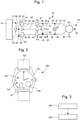
- the crystal oscillator 10 comprises a crystal resonator 12.
- the crystal resonator 12 typically comprises a quartz crystal.
- the crystal oscillator 10 further comprises an electronic oscillator circuit 14 electrically connected to the crystal resonator 12.
- the crystal resonator 12 and the electronic oscillator circuit 14 are connected in parallel.
- the electronic oscillator circuit 14 comprises an output terminal 50 by way of which a well-defined and frequency stabilized clock signal synchronized to the resonance frequency of the crystal resonator 12 can be provided.
- the crystal oscillator 10 further comprises first and second capacitors 21, 22.
- the first and second capacitors 21, 22 are connected to respective input and output terminals 47, 49 of the electronic oscillator circuit 14.
- the first capacitor 21 comprises a second terminal 25 electrically connected to a first input terminal 47 of the electronic oscillator circuit 14.
- the second capacitor 22 comprises a second terminal 26 electrically connected to a second output terminal 49 of the electronic oscillator circuit.
- the crystal resonator 12 comprises a first terminal 27.
- the first terminal 27 being electrically connected to the second terminal 25 and through the first input terminal 47.
- the second terminal 29 of the crystal resonator 12 is electrically connected to the second terminal 26 of the second capacitor 22 and to the second output terminal 49 of the electronic oscillator circuit 14.
- the crystal oscillator 10 further comprises a switch 30.
- the switch 30 may be implemented as a MOS transistor.
- the switch 30 comprises a first terminal 31, a second terminal 32 and at least a third terminal 33.
- First and second terminals 31, 32 are implemented by the source and drain of the transistor.
- the third terminal 33 is implemented by a gate of the transistor or switch 30.
- the first terminal 31 of the switch 30 is connected to a first terminal 23 of the first capacitor 21.
- the second terminal 32 of the switch 30 is connected to a first terminal 24 of the second capacitor 22.
- the first and second capacitors 21, 22 are operable to inject a driving frequency into the crystal resonator 12 and/or into the electronic oscillator circuit 14.
- the capacitors 21, 22 are typically driven by a phase signal provided by a phase output 17 of a startup controller 16.
- the startup controller 16 serves to provide phase shifted driving signals to the first and second capacitors 21, 22, at least during a startup phase of a startup procedure of the crystal oscillator 10.
- the switch 30 is configured to switch the crystal oscillator 10 between a startup mode and a driving mode.
- the startup mode the first and second capacitors 21, 22 are frequently charged and discharged by the startup controller 16.
- the driving mode the first and second capacitors 21, 22 are effectively decoupled from the startup controller 16.
- the switch 30 In the startup mode the switch 30 is opened, hence the conductivity between the first terminal 31 and the second terminal 32 of the switch 38 is comparatively low. Switching of the switch 30 leads to an increase of the conductivity between the first and the second terminals 31, 32. In this way the impedance seen by the electronic oscillator circuit 14 can be reduced and power consumption of the crystal oscillator during the startup phase can be reduced significantly.
- the startup controller 16 comprises the phase output 17 and a startup control output 18.
- the phase output 17 provide an oscillating phase signal with a frequency, typically in the range of the frequency of the crystal resonator 12.
- the startup control output 18 provides a startup control signal.
- the startup control signal can be either a logical one or a logical zero. If the startup control signal provided at the startup control output 18 is high or equals a logical one, the crystal oscillator 10 is in the startup mode. If the signal at the startup control output 18 is zero or low the crystal oscillator 10 is in the driving mode.
- the third terminal 33 of the switch 30 connected to the startup control output 18 via an inverter 62.
- the switch 30 is effectively switched off when the startup control signal at the startup control output 18 is high.
- the switch 30 is turned on when the startup control signal at the startup control output 18 is low or zero.
- the crystal oscillator 10 further comprises a first logic gate 51 and a second logic gate 52.
- First and second logic gates 51, 52 are both implemented as logical AND gates.
- the first logic gate 51 comprises a first input terminal 53 connected to the phase output 17 of the startup controller 16.
- a second input terminal 55 is connected to the startup control output 18 of the startup controller 16.
- the second logic gate 52 comprises a first input terminal 54 and a second input terminal 56.
- the second input terminal 56 is connected to the startup control output 18 of the startup controller 16.
- the first input terminal 54 is connected to the phase output 17 of the startup controller 16 via another inverter 60.
- the output terminal 57 of the first logic gate 51 is connected to an input terminal 43 of a first buffer amplifier 41.
- a respective output 45 of the first buffer amplifier 41 is connected to the first terminal 31 of the switch 30 and to the first terminal 23 of the first capacitor 21.
- a second buffer amplifier 42 there is provided a second buffer amplifier 42.
- An input terminal 44 of the second buffer amplifier 42 is connected to an output 58 of the second logic gate 52.
- the output terminal 46 of the second buffer amplifier 42 is connected to the second terminal 32 of the switch 30 and to the first terminal 24 of the second capacitor 22.
- the buffer amplifier is 41, 42 the incident impedance as seen by the crystal resonator 12 can be kept substantially constant for each operation mode of the crystal oscillator. In this way a rather constant and stable frequency output can be provided at the output terminal 50 of the electronic oscillator circuit 14.
- the implementation of two logic AND gates 51, 52 and the coupling of the second input terminals 55, 56 of the logic gates 51, 52 with the startup control output 18 together with the inverted coupling of the third terminal 33 of the switch 30 to the startup control output 18 provides a concurrent switching behavior.
- the switch 30 is effectively switched off, hence when the startup control signal provided at the startup control output is high the first and second logic gates 51, 52 provide phase shifted first and second phase signals by way of which the first and second buffer amplifier 41, 42 can be driven and by way of which the first and second capacitors 21, 22 can be charged and discharged, respectively.
- FIG. 2 an example of a portable electronic device 100 implemented as a wristwatch is illustrated.
- the portable electronic device 100 comprises a housing 110 and a wristband 103.
- the electronic device 100 is further provided with a clockwork mechanism 105 connected or coupled with a display 102.
- the electronic device is further equipped with an electronic energy source 104, such as a battery and with a crystal oscillator 10 as described above.
- the crystal oscillator 10 provides a well-defined, frequency-stabilized and hence a rather precise clock signal.
- a flowchart of a method of initiating operation of a crystal oscillator as described above is schematically illustrated.
- the method makes use of the crystal oscillator 10 as described above in connection with Fig. 1 .
- a first step 200 the crystal oscillator 10 is operated in a startup mode.
- first and second phase signals are provided to first and second capacitors 21, 22 of the crystal oscillator 10.
- the electronic oscillator circuit 14 starts to oscillate the crystal oscillator 10 is switched into a driving mode by making use of the switch 30 of the crystal oscillator.
- Switching of the crystal oscillator from the startup mode into the driving mode is typically governed by the startup controller 16 as the electronic oscillator circuit 14 starts to oscillate. For this, there may be provided a feedback (not illustrated) from the electronic oscillator circuit 14 to the startup controller 16.
Landscapes
- Oscillators With Electromechanical Resonators (AREA)
Priority Applications (4)
| Application Number | Priority Date | Filing Date | Title |
|---|---|---|---|
| EP20194779.3A EP3965290A1 (de) | 2020-09-07 | 2020-09-07 | Kristalloszillator und startverfahren für einen kristalloszillator |
| US17/341,484 US11245362B1 (en) | 2020-09-07 | 2021-06-08 | Crystal oscillator and startup method for a crystal oscillator |
| JP2021104645A JP7198875B2 (ja) | 2020-09-07 | 2021-06-24 | 結晶式発振器、及び結晶式発振器の始動方法 |
| CN202110869845.4A CN114157289B (zh) | 2020-09-07 | 2021-07-30 | 晶体振荡器和晶体振荡器的启动方法 |
Applications Claiming Priority (1)
| Application Number | Priority Date | Filing Date | Title |
|---|---|---|---|
| EP20194779.3A EP3965290A1 (de) | 2020-09-07 | 2020-09-07 | Kristalloszillator und startverfahren für einen kristalloszillator |
Publications (1)
| Publication Number | Publication Date |
|---|---|
| EP3965290A1 true EP3965290A1 (de) | 2022-03-09 |
Family
ID=72422114
Family Applications (1)
| Application Number | Title | Priority Date | Filing Date |
|---|---|---|---|
| EP20194779.3A Pending EP3965290A1 (de) | 2020-09-07 | 2020-09-07 | Kristalloszillator und startverfahren für einen kristalloszillator |
Country Status (4)
| Country | Link |
|---|---|
| US (1) | US11245362B1 (de) |
| EP (1) | EP3965290A1 (de) |
| JP (1) | JP7198875B2 (de) |
| CN (1) | CN114157289B (de) |
Cited By (1)
| Publication number | Priority date | Publication date | Assignee | Title |
|---|---|---|---|---|
| EP4415267A1 (de) | 2023-02-10 | 2024-08-14 | The Swatch Group Research and Development Ltd | Verfahren zum betrieb eines schnellstart-oszillatorsystems und schnellstart-oszillatorsystem |
Citations (2)
| Publication number | Priority date | Publication date | Assignee | Title |
|---|---|---|---|---|
| US20070030085A1 (en) * | 2005-03-24 | 2007-02-08 | Cypress Semiconductor Corp. | Regulated Capacitive Loading and Gain Control of a Crystal Oscillator During Startup and Steady State Operation |
| WO2007060210A1 (en) * | 2005-11-24 | 2007-05-31 | Telefonaktiebolaget L M Ericsson (Publ) | Oscillator comprising a startup control device |
Family Cites Families (12)
| Publication number | Priority date | Publication date | Assignee | Title |
|---|---|---|---|---|
| JPS56160682A (en) * | 1980-05-15 | 1981-12-10 | Citizen Watch Co Ltd | Electronic watch |
| US5150081A (en) * | 1991-02-28 | 1992-09-22 | Adaptec, Inc. | Integrated crystal oscillator with circuit for limiting crystal power dissipation |
| JP3829525B2 (ja) * | 1998-04-02 | 2006-10-04 | セイコーエプソン株式会社 | 容量アレイユニット及び発振回路 |
| EP1289121A1 (de) * | 2001-08-13 | 2003-03-05 | EM Microelectronic-Marin SA | Inverteroszillatorschaltung mit niedrigem Verbrauch |
| EP1429451A1 (de) | 2002-12-11 | 2004-06-16 | Dialog Semiconductor GmbH | Parallelresonanzoszillator mit hoher Qualität |
| US7075381B2 (en) * | 2003-04-15 | 2006-07-11 | Nihon Dempa Kogyo Co., Ltd. | Oscillator circuit and oscillator |
| JP2006295362A (ja) | 2005-04-07 | 2006-10-26 | Matsushita Electric Ind Co Ltd | 電圧制御発振回路用の印加電圧制御回路 |
| JP5757786B2 (ja) * | 2011-01-06 | 2015-07-29 | 日本電波工業株式会社 | 水晶発振器 |
| JP6013070B2 (ja) | 2012-07-31 | 2016-10-25 | ルネサスエレクトロニクス株式会社 | 半導体装置及びその制御方法 |
| EP3487069B1 (de) * | 2017-11-17 | 2020-01-01 | Axis AB | Kristalloszillatorschaltung |
| US11082006B2 (en) * | 2019-01-23 | 2021-08-03 | Stmicroelectronics International N.V. | Low power crystal oscillator |
| EP3965291B1 (de) | 2020-09-07 | 2024-08-14 | The Swatch Group Research and Development Ltd | Kristalloszillator und startverfahren für einen kristalloszillator |
-
2020
- 2020-09-07 EP EP20194779.3A patent/EP3965290A1/de active Pending
-
2021
- 2021-06-08 US US17/341,484 patent/US11245362B1/en active Active
- 2021-06-24 JP JP2021104645A patent/JP7198875B2/ja active Active
- 2021-07-30 CN CN202110869845.4A patent/CN114157289B/zh active Active
Patent Citations (2)
| Publication number | Priority date | Publication date | Assignee | Title |
|---|---|---|---|---|
| US20070030085A1 (en) * | 2005-03-24 | 2007-02-08 | Cypress Semiconductor Corp. | Regulated Capacitive Loading and Gain Control of a Crystal Oscillator During Startup and Steady State Operation |
| WO2007060210A1 (en) * | 2005-11-24 | 2007-05-31 | Telefonaktiebolaget L M Ericsson (Publ) | Oscillator comprising a startup control device |
Non-Patent Citations (1)
| Title |
|---|
| SCHOLL MARKUS ET AL: "A 32 MHz Crystal Oscillator with Fast Start-Up Using Dithered Injection and Negative Resistance Boost", ESSCIRC 2019 - IEEE 45TH EUROPEAN SOLID STATE CIRCUITS CONFERENCE (ESSCIRC), IEEE, 23 September 2019 (2019-09-23), pages 49 - 52, XP033660851, DOI: 10.1109/ESSCIRC.2019.8902894 * |
Cited By (1)
| Publication number | Priority date | Publication date | Assignee | Title |
|---|---|---|---|---|
| EP4415267A1 (de) | 2023-02-10 | 2024-08-14 | The Swatch Group Research and Development Ltd | Verfahren zum betrieb eines schnellstart-oszillatorsystems und schnellstart-oszillatorsystem |
Also Published As
| Publication number | Publication date |
|---|---|
| JP2022044552A (ja) | 2022-03-17 |
| US11245362B1 (en) | 2022-02-08 |
| CN114157289B (zh) | 2025-08-26 |
| CN114157289A (zh) | 2022-03-08 |
| JP7198875B2 (ja) | 2023-01-04 |
Similar Documents
| Publication | Publication Date | Title |
|---|---|---|
| US5126695A (en) | Semiconductor integrated circuit device operated with an applied voltage lower than required by its clock oscillator | |
| EP0905877A1 (de) | Oszillatorschaltung, elektronische schaltung, halbleiterbauelement, elektronische anordnung und uhr | |
| US4321562A (en) | Crystal oscillator circuit capable of changing the number of inverter stages coupled in series | |
| EP0483254A1 (de) | Quarzoszillator mit verschiedenen bandbreiten | |
| EP0593069B1 (de) | Umschaltbare Kompensation für verbesserte Leistung eines Oszillators | |
| US8988159B2 (en) | Oscillator and IC chip | |
| US11245362B1 (en) | Crystal oscillator and startup method for a crystal oscillator | |
| CN116545385A (zh) | 晶体振荡电路及其起振方法 | |
| USRE39329E1 (en) | Oscillation circuit, electronic circuit using the same, and semiconductor device, electronic equipment, and timepiece using the same | |
| US4389704A (en) | Power source supply system | |
| KR100239105B1 (ko) | 전압 레벨 시프팅 회로를 갖는 저 전압, 저 전력 발진기 | |
| HK40063333A (en) | Crystal oscillator and startup method for a crystal oscillator | |
| HK40063333B (zh) | 晶体振荡器和晶体振荡器的启动方法 | |
| JP2004304253A (ja) | 発振器とこれを用いた電子機器 | |
| US20240022211A1 (en) | Semiconductor device | |
| US11664752B2 (en) | Method for controlling electronic watch and electronic watch | |
| US20020075090A1 (en) | Oscillation control circuit | |
| US4095407A (en) | Oscillating and dividing circuit having level shifter for electronic timepiece | |
| JPH11284438A (ja) | 圧電発振器 | |
| JP3612929B2 (ja) | 発振回路、これを用いた電子回路、これらを用いた半導体装置、電子機器および時計 | |
| US20090033434A1 (en) | Oscillation circuit | |
| JP4963764B2 (ja) | 電子時計 | |
| CN116938146A (zh) | 晶体振荡器电路及晶体振荡方法 | |
| JP2712746B2 (ja) | 発振回路 | |
| JP2002016437A (ja) | 圧電発振器 |
Legal Events
| Date | Code | Title | Description |
|---|---|---|---|
| PUAI | Public reference made under article 153(3) epc to a published international application that has entered the european phase |
Free format text: ORIGINAL CODE: 0009012 |
|
| STAA | Information on the status of an ep patent application or granted ep patent |
Free format text: STATUS: THE APPLICATION HAS BEEN PUBLISHED |
|
| AK | Designated contracting states |
Kind code of ref document: A1 Designated state(s): AL AT BE BG CH CY CZ DE DK EE ES FI FR GB GR HR HU IE IS IT LI LT LU LV MC MK MT NL NO PL PT RO RS SE SI SK SM TR |
|
| STAA | Information on the status of an ep patent application or granted ep patent |
Free format text: STATUS: REQUEST FOR EXAMINATION WAS MADE |
|
| 17P | Request for examination filed |
Effective date: 20220909 |
|
| RBV | Designated contracting states (corrected) |
Designated state(s): AL AT BE BG CH CY CZ DE DK EE ES FI FR GB GR HR HU IE IS IT LI LT LU LV MC MK MT NL NO PL PT RO RS SE SI SK SM TR |
|
| P01 | Opt-out of the competence of the unified patent court (upc) registered |
Effective date: 20230615 |
|
| STAA | Information on the status of an ep patent application or granted ep patent |
Free format text: STATUS: EXAMINATION IS IN PROGRESS |
|
| 17Q | First examination report despatched |
Effective date: 20240215 |
|
| GRAP | Despatch of communication of intention to grant a patent |
Free format text: ORIGINAL CODE: EPIDOSNIGR1 |
|
| STAA | Information on the status of an ep patent application or granted ep patent |
Free format text: STATUS: GRANT OF PATENT IS INTENDED |
|
| INTG | Intention to grant announced |
Effective date: 20260313 |