EP3965321B1 - Vorrichtung und verfahren zur anpassung der leistung eines drahtlosen signals - Google Patents
Vorrichtung und verfahren zur anpassung der leistung eines drahtlosen signals Download PDFInfo
- Publication number
- EP3965321B1 EP3965321B1 EP20837265.6A EP20837265A EP3965321B1 EP 3965321 B1 EP3965321 B1 EP 3965321B1 EP 20837265 A EP20837265 A EP 20837265A EP 3965321 B1 EP3965321 B1 EP 3965321B1
- Authority
- EP
- European Patent Office
- Prior art keywords
- transmitting channel
- signal
- radio frequency
- frequency signal
- adjusting
- Prior art date
- Legal status (The legal status is an assumption and is not a legal conclusion. Google has not performed a legal analysis and makes no representation as to the accuracy of the status listed.)
- Active
Links
Images



Classifications
-
- H—ELECTRICITY
- H04—ELECTRIC COMMUNICATION TECHNIQUE
- H04B—TRANSMISSION
- H04B17/00—Monitoring; Testing
- H04B17/10—Monitoring; Testing of transmitters
- H04B17/11—Monitoring; Testing of transmitters for calibration
- H04B17/12—Monitoring; Testing of transmitters for calibration of transmit antennas, e.g. of the amplitude or phase
-
- H—ELECTRICITY
- H04—ELECTRIC COMMUNICATION TECHNIQUE
- H04B—TRANSMISSION
- H04B17/00—Monitoring; Testing
- H04B17/10—Monitoring; Testing of transmitters
- H04B17/15—Performance testing
- H04B17/17—Detection of non-compliance or faulty performance, e.g. response deviations
-
- H—ELECTRICITY
- H03—ELECTRONIC CIRCUITRY
- H03F—AMPLIFIERS
- H03F1/00—Details of amplifiers with only discharge tubes, only semiconductor devices or only unspecified devices as amplifying elements
- H03F1/56—Modifications of input or output impedances, not otherwise provided for
-
- H—ELECTRICITY
- H03—ELECTRONIC CIRCUITRY
- H03F—AMPLIFIERS
- H03F3/00—Amplifiers with only discharge tubes or only semiconductor devices as amplifying elements
- H03F3/20—Power amplifiers, e.g. Class B amplifiers, Class C amplifiers
- H03F3/24—Power amplifiers, e.g. Class B amplifiers, Class C amplifiers of transmitter output stages
-
- H—ELECTRICITY
- H04—ELECTRIC COMMUNICATION TECHNIQUE
- H04B—TRANSMISSION
- H04B17/00—Monitoring; Testing
- H04B17/10—Monitoring; Testing of transmitters
- H04B17/101—Monitoring; Testing of transmitters for measurement of specific parameters of the transmitter or components thereof
- H04B17/103—Reflected power, e.g. return loss
-
- H—ELECTRICITY
- H04—ELECTRIC COMMUNICATION TECHNIQUE
- H04B—TRANSMISSION
- H04B17/00—Monitoring; Testing
- H04B17/10—Monitoring; Testing of transmitters
- H04B17/101—Monitoring; Testing of transmitters for measurement of specific parameters of the transmitter or components thereof
- H04B17/104—Monitoring; Testing of transmitters for measurement of specific parameters of the transmitter or components thereof of other parameters, e.g. DC offset, delay or propagation times
-
- H—ELECTRICITY
- H04—ELECTRIC COMMUNICATION TECHNIQUE
- H04B—TRANSMISSION
- H04B17/00—Monitoring; Testing
- H04B17/10—Monitoring; Testing of transmitters
- H04B17/15—Performance testing
- H04B17/18—Monitoring during normal operation
-
- H—ELECTRICITY
- H04—ELECTRIC COMMUNICATION TECHNIQUE
- H04L—TRANSMISSION OF DIGITAL INFORMATION, e.g. TELEGRAPHIC COMMUNICATION
- H04L27/00—Modulated-carrier systems
- H04L27/26—Systems using multi-frequency codes
- H04L27/2601—Multicarrier modulation systems
- H04L27/2614—Peak power aspects
-
- H—ELECTRICITY
- H04—ELECTRIC COMMUNICATION TECHNIQUE
- H04M—TELEPHONIC COMMUNICATION
- H04M1/00—Substation equipment, e.g. for use by subscribers
- H04M1/24—Arrangements for testing
Definitions
- the present invention relates to electromagnetic compatibility technology, for example, to a wireless signal performance adjustment apparatus and method and a wireless communication terminal.
- a computing device includes one or more central processing units (CPU), input/output interfaces, network interfaces, and memories.
- CPU central processing units
- input/output interfaces input/output interfaces
- network interfaces network interfaces
- memories memories
- the memories may include a non-permanent memory, a random access memory (RAM), and/or a non-volatile memory in the computer-readable medium, such as a read-only memory (ROM) or a flash RAM.
- RAM random access memory
- ROM read-only memory
- flash RAM flash random access memory
- the internal storage is an example of the computer-readable medium.
- the computer-readable medium including permanent computer-readable medium and non-permanent computer-readable medium, removable and non-removable media, may implement information storage by any method or technology.
- the information may be a computer-readable instruction, a data structure, a module of program, or other data.
- Examples of the computer storage medium include, but not limited to, a phase-change random access memory (PRAM), a static random access memory (SRAM), a dynamic random access memory (DRAM), other types of random access memory (RAM), the read-only memory (ROM), an electrically erasable programmable read-only memory (EEPROM), a flash memory or other memory technologies, a compact disc read-only memory (CD-ROM), a digital video disk (DVD) or other optical storage, a magnetic cassette, a magnetic tape magnetic disk storage or other magnetic storage devices or any other non-transmission medium, which may be used to store the information accessible by the computing device.
- the computer-readable medium does not include a non-temporary computer-readable medium (transitory media) such as a modulated data signal and a carrier wave.
- a transmitting frequency and a receiving frequency are different, and a power amplifier of a transmitting channel may not only generate a signal in a transmitting frequency band, but also generate an interference signal within a receiving frequency band.
- these interference signals within the receiving frequency band are noises, which are generally called a receive band noise (RxBN), thus the smaller the RxBN is, the better it is.
- the power amplifier on the transmitting channel may also generate harmonic signals, which needs to be strictly limited. There are strict requirements for intensity of a harmonic in a variety of electromagnetic compatibility (EMC) test specifications.
- EMC electromagnetic compatibility
- Both the RxBN and the harmonic come from the power amplifier, and these two indexes are closely related to a load impedance of the power amplifier. Different load impedances correspond to different RxBN and harmonic characteristics. Therefore, the power amplifier may usually have specific loadpull information (also called loadpull diagram).
- loadpull information also called loadpull diagram.
- a specific radio frequency impedance position may be selected according to the loadpull, but only if a position of a radio frequency test socket is connected with a radio frequency instrument having a load impedance of 50 ⁇ .
- an impedance of the position of the radio frequency test socket may change in real time with an application scenario, that is, the load impedance of the power amplifier may also change accordingly, which may cause deterioration of the RxBN and the harmonic.
- the present invention proposes to notice an abnormal state by monitoring a transmission indicator of the transmitting channel in real time, and adjust the transmission performance of the transmitting channel by adjusting the power amplifier, such as adjusting a transmitting power of the power amplifier, adjusting a matching of the power amplifier, or reducing a peak-to-average ratio of a transmitted signal, or adjusting a matching of the antenna, so as to reduce an electromagnetic interference signal radiated by the wireless communication terminal, thereby improving the electromagnetic compatibility performance of the wireless communication terminal, and thus meeting the electromagnetic compatibility performance requirement of the wireless communication terminal in a complex and changeable actual use scenario.
- adjusting the power amplifier such as adjusting a transmitting power of the power amplifier, adjusting a matching of the power amplifier, or reducing a peak-to-average ratio of a transmitted signal, or adjusting a matching of the antenna
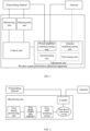
- FIG. 1 is a schematic diagram illustrating a composition and structure of a wireless signal performance adjustment apparatus provided by an embodiment of the present invention.
- the wireless signal performance adjustment apparatus at least includes: a monitoring unit, a control unit, a measurement unit and an adjustment unit; where the monitoring unit is configured to monitor a radio frequency signal of a transmitting channel; the control unit is configured to receive the radio frequency signal of the transmitting channel from the monitoring unit, control the measurement unit to perform measurement if the radio frequency signal of the transmitting channel does not meet a performance requirement condition, and determine adjustment information according to a load impedance from the measurement unit; the measurement unit is configured to measure a load impedance of a power amplifier in the transmitting channel under the control of the control unit; and the adj ustment unit is configured to adjust the transmitting channel according to the adjustment information under the control of the control unit, so that the radio frequency signal of the transmitting channel meets the performance requirement condition.
- the monitoring unit is configured to monitor a transmitting channel of a wireless communication terminal in real time to obtain the radio frequency signal of the transmitting channel.
- the radio frequency signal of the transmitting channel is also obtained by monitoring the transmitting channel of the wireless communication terminal according to a preset period or within a specified time period.
- the adjustment unit includes at least one of the following modules: a power amplifier matching and tuning module configured to adjust matching of the power amplifier in the transmitting channel, so that the radio frequency signal of the transmitting channel meets the performance requirement condition; an antenna matching and tuning module configured to adjust an impedance matching between the transmitting channel and an antenna, so that the radio frequency signal of the transmitting channel meets the performance requirement condition; a first tuning module configured to adjust a peak-to-average ratio of a transmitted signal in the transmitting channel, so that the radio frequency signal of the transmitting channel meets the performance requirement condition; and a second tuning module configured to adjust a transmitting power so that the radio frequency signal of the transmitting channel meets the performance requirement condition.
- a power amplifier matching and tuning module configured to adjust matching of the power amplifier in the transmitting channel, so that the radio frequency signal of the transmitting channel meets the performance requirement condition
- an antenna matching and tuning module configured to adjust an impedance matching between the transmitting channel and an antenna, so that the radio frequency signal of the transmitting channel meets the performance requirement condition
- a first tuning module
- the adjustment unit includes the power amplifier matching tuning module; or, the adjustment unit includes the power amplifier matching tuning module and the antenna matching tuning module; or, the adjustment unit includes the power amplifier matching tuning module, the antenna matching tuning module and the first tuning module; or, the adjustment unit includes the power amplifier matching tuning module, the antenna matching tuning module, the first tuning module and the second tuning module.
- Not meeting the performance requirement condition includes not meeting an electromagnetic compatibility performance requirement.
- the present invention detects an abnormal state by monitoring a transmission indicator of the transmitting channel in real time, and realizes adjustment of the transmission performance of the transmitting channel by adjusting the power amplifier, so as to reduce electromagnetic interference signals radiated by the wireless communication terminal, thereby improving the electromagnetic compatibility performance of the wireless communication terminal, such that the wireless communication terminal in a complex and changeable actual use scenario meets the electromagnetic compatibility performance requirement.
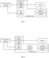
- FIG. 2 is a schematic diagram illustrating a composition and structure of a monitoring unit according to an embodiment of the present invention.
- the monitoring unit at least includes a coupler, a first down-conversion circuit, a first analog-to-digital converter (ADC) sampling circuit, a first digital variable gain amplifier and a first digital processing unit;
- the coupler is configured to obtain the radio frequency signal by coupling from the transmitting channel and output the radio frequency signal to the first down-conversion circuit;
- the first down-conversion circuit is configured to process the radio frequency signal obtained by coupling according to a preset frequency so as to obtain a low-frequency signal at a required frequency point;
- the first ADC sampling circuit is configured to perform analog-to-digital conversion on the low-frequency signal to obtain a digital signal;
- the first digital variable gain amplifier is configured to amplify the digital signal obtained by the analog-to-digital conversion so that the amplified digital signal is in a range that the first digital processing unit process.
- the first digital processing unit is configured to calculate an amplitude of an amplified digital signal so as to obtain a signal strength of the transmitting channel at a required frequency point, and output the obtained signal strength of the transmitting channel to the control unit.
- the required frequency point is a frequency point for determining an over-standard position, and for a second harmonic, a frequency point of the second harmonic is the required frequency point.
- the coupler may share a broadband bidirectional coupler included in the transmitting channel of the mobile terminal, or the monitoring unit may use a broadband coupler alone.
- a local oscillator frequency of the first down-conversion circuit may be arbitrarily selected, such as a transmission center frequency, or a double frequency of the transmission center frequency, or a triple frequency of the transmission center frequency.
- the first digital processing unit is configured to: perform a Fourier transform on a digital signal output from the first digital variable gain amplifier to obtain a corresponding relationship between a frequency and a signal amplitude; and add a gain value of the first digital variable gain amplifier and a coupling degree of the coupler to an obtained signal amplitude to obtain the signal strength at the required frequency point.
- FIG. 3 is a schematic diagram illustrating a composition and structure of a measurement unit provided by an embodiment of the present invention.
- the measurement unit at least includes: a bidirectional coupler, a channel selection circuit, a second down-conversion circuit, a second ADC sampling circuit, a second digital variable gain amplifier and a second digital processing unit; where the bidirectional coupler is configured to couple a reference signal transmitted in a transmitting channel to obtain a coupled signal; and the channel selection circuit is configured to receive the coupled signal of a forward signal through a first channel and receive the coupled signal of a reflected signal through a second channel. When a VSWR measurement is required, the channel selection circuit switches the first channel and the second channel once respectively.
- the second down-conversion circuit is configured to process the coupled signal according to a preset frequency so as to obtain a first low-frequency signal with a required frequency; and process the reflected signal according to the preset frequency to obtain a second low-frequency signal with the required frequency, where the preset frequency is the required frequency.
- the second ADC sampling circuit is configured to perform an analog-to-digital conversion on the first low-frequency signal to obtain a first digital signal; and perform the analog-to-digital conversion on the second low-frequency signal to obtain a second digital signal.
- the second digital variable gain amplifier is configured to amplify the first digital signal, so that the amplified first digital signal is within a range that the second digital processing unit process; and amplify the second digital signal so that the amplified second digital signal is within a range that the second digital processing unit process.
- the second digital processing unit is configured to determine a current load impedance value of the power amplifier according to the obtained first digital signal and second digital signal.
- the second digital processing unit is configured to: perform calculation based on the first digital signal to obtain a first signal strength and first phase information of the coupled signal, and perform calculation based on the second digital signal to obtain a second signal strength and second phase information of the coupled signal; calculate a ratio of the first signal strength to the second signal strength to obtain a voltage standing wave ratio (VSWR), and obtain phase information of an impedance according to a difference between the first phase information and the second phase information; and calculate the current load impedance value of the power amplifier according to the VSWR, the phase information of the impedance and a scattering parameter stored in a memory, and output the obtained load impedance value to the control unit.
- VSWR voltage standing wave ratio
- the scattering parameter stored in the memory is real-time impedance information of a current circuit. After the adjustment unit performs matching adjustment on the corresponding circuit, the scattering parameter can be updated accordingly.
- the channel selection circuit may be a double-pole double-throw switch or a similar functional circuit built by a single-pole double-throw switch.
- the monitoring unit and the measurement unit are two independent functional units, but a circuit in the monitoring unit with the same functions as that in the measurement unit is multiplexed, that is, only one set of circuits is provided in the wireless signal performance apparatus, such as the first down-conversion circuit and the second down-conversion circuit, the first ADC sampling circuit and the second ADC sampling circuit, the first digital variable gain amplifier and the second digital variable gain amplifier, etc.
- a set of circuits with the same function in the monitoring unit and the measuring unit is also provided respectively.
- FIG. 4 is a schematic diagram illustrating a composition and structure of a control unit according to an embodiment of the present invention.
- the control unit at least includes a first processing module, a second processing module, a control module and a storage module storing loadpull information, where the first processing module is configured to receive a signal of the transmitting channel from the monitoring unit, and control the measurement unit to perform measurement if the radio frequency signal of the transmitting channel does not meet the performance requirement condition; the second processing module is configured to query optimal impedance position information and calculate the adjustment information according to the loadpull information of the power amplifier, based on a value of the load impedance from the measurement unit; and the control module is configured to control the adjustment unit to adjust the transmitting channel according to the obtained adjustment information, and update a scattering parameter in the memory according to an adjustment result.
- the adjustment information includes the amount of tuning change in a tuning part, a capacitance change of an adjustable capacitor, an inductance change of an adjustable inductor.
- a method of calculating the adjustment information is related to the number of devices with adjustable impedance in the matching circuit. If the adjustment is successfully completed, that is, if it is determined that the radio frequency signal of the transmitting channel meets the performance requirement condition, the final numerical information of adjustable devices may be updated to the memory for convenience of future debugging and use.
- the method of calculating the adjustment information may include: an adjustment of a parallel circuit may be performed according to an addition and subtraction of an admittance, and an adjustment of a series circuit may be performed according to an addition and subtraction of an impedance.
- FIG. 5 is schematic diagram illustrating a composition and structure of an adjustment unit according to an embodiment of the present invention.
- the adjustment unit includes a power amplifier matching tuning module configured to: adjust a transmitting channel according to the obtained adjustment information under the control of a control unit, and tune a load impedance of a power amplifier to match with a current antenna to adapt to a position to achieve the best RxBN and harmonic, so that the radio frequency signal of the transmitting channel meets a performance requirement condition.
- the power amplifier matching tuning module may realize tuning by using a variables inductance or a variables capacitance, and may also use a switch to perform different matching selections to achieve the function of tuning.
- the adjustment information includes the amount of tuning change in a tuning part, such as a capacitance change of an adjustable capacitor, an inductance change of an adjustable inductor, and the like.
- FIG. 6 is a schematic diagram illustrating a composition and structure of another adjustment unit according to an embodiment of the present invention. As shown in FIG. 6 , the adjustment unit includes a power amplifier matching tuning module and an antenna matching tuning module.
- the antenna matching tuning module when the adjustment of the power amplifier matching tuning module fails to achieve the purpose, that is, when the radio frequency signal of the transmitting channel still does not meet the performance requirement condition, the antenna matching tuning module is activated for adjustment.
- the antenna matching tuning module is configured to adjust impedance matching between the transmitting channel and an antenna according to impedance position information stored in a memory, so that the radio frequency signal of the transmitting channel meets the performance requirement condition.
- the power amplifier matching tuning module is the same as that in the previous embodiment, which is not repeated here.
- FIG. 7 is a schematic diagram illustrating a composition and structure of another adjustment unit according to an embodiment of the present invention.
- the adjustment unit includes a power amplifier matching tuning module, an antenna matching tuning module and a first tuning module.
- the first tuning module when the adjustment of the antenna matching tuning circuit fails to achieve the purpose, that is, when the radio frequency signal of the transmitting channel still does not meet the performance requirement condition, the first tuning module is activated for adjustment by adjusting a peak-to-average ratio of the transmitted signal
- the first tuning module is configured to adjust the peak-to-average ratio of the transmitted signal in the transmitting channel, so that the radio frequency signal of the transmitting channel meets the performance requirement condition.
- the power amplifier matching tuning module and the antenna matching tuning module are the same as those in the previous embodiment, which are not repeated here.
- the function of the first tuning module belongs to a modem, which may be set in a control unit.
- FIG. 8 is a schematic diagram illustrating a composition and structure of another adjustment unit according to an embodiment of the present invention.
- the adjustment unit includes a power amplifier matching tuning module, an antenna matching tuning module, a first tuning module and a second tuning module.
- the second tuning module is configured to adjust a transmitting power so that the radio frequency signal of the transmitting channel meets the performance requirement condition.
- the second tuning module when the adjustment of the peak-to-average ratio of the transmitted signal fails to achieve the purpose, that is, when the radio frequency signal of the transmitting channel still does not meet the performance requirement condition, the second tuning module is activated for adjustment by adjusting the transmitting power and gradually reduce the transmitting power.
- the function of the first tuning module and the second tuning module belongs to a modem, which may be set in a control unit.
- the present invention further provides a wireless communication terminal, which includes the wireless signal performance adjustment apparatus according to any embodiment of the present invention.
- FIG. 9 is a schematic flow chart illustrating a wireless signal performance adjustment method according to an embodiment of the present invention. As shown in FIG. 9 , the method includes: Step 900: obtaining a radio frequency signal of a transmitting channel of a wireless communication terminal.
- the radio frequency signal of the transmitting channel is obtained by monitoring the transmitting channel of the wireless communication terminal in real time.
- the radio frequency signal of the transmitting channel is also obtained by monitoring the transmitting channel of the wireless communication terminal according to a preset period or within a specified time period.
- Step 901 determining that the radio frequency signal of the transmitting channel does not meet a performance requirement condition according to the obtained radio frequency signal of the transmitting channel, and measuring a load impedance of a power amplifier in the transmitting channel.
- Not meeting the performance requirement condition includes not meeting an electromagnetic compatibility performance requirement.
- determining that the radio frequency signal of the transmitting channel does not meet the performance requirement condition according to the obtained radio frequency signal of the transmitting channel includes: monitoring, according to a frequency point of a spurious signal, a signal strength at the frequency point of the transmitting channel. When the obtained signal strength exceeds a certain threshold, it is determined that the radio frequency signal of the transmitting channel does not meet the performance requirement condition, which means that there is an electromagnetic compatibility risk in the wireless communication terminal.
- the frequency point of the spurious signal is also the position of the spurious signal. According to the EMC specification, there are different EMC requirements for different frequency points. Therefore, according to the present invention, during monitoring, it is necessary to determine the measured frequency point first, and then measure this position.
- the step of determining the obtained radio frequency signal of the transmitting channel of the wireless communication terminal is continued to proceed.
- measuring the load impedance of the power amplifier in the transmitting channel includes: coupling a reference signal transmitted in the transmitting channel; processing the coupled signal obtained by coupling according to a preset frequency so as to obtain a first digital signal, and processing a reflected signal emitted by the coupled signal according to the preset frequency to obtain a second digital signal; and determining a value of the load impedance of the power amplifier according to the obtained first digital signal and the obtained second digital signal.
- the processing of the coupled signal obtained by coupling or the reflected signal includes: performing a down-conversion processing, an analog-to-digital conversion and an amplification processing.
- determining the current load impedance value of the power amplifier according to the obtained first digital signal and second digital signal includes: performing calculation based on the first digital signal to obtain a first signal strength and first phase information of the coupled signal, and performing calculation based on the second digital signal to obtain a second signal strength and second phase information of the coupled signal (where before performing calculation based on the first digital signal or the second digital signal, the method further includes amplifying the first digital signal and amplifying the second digital signal); calculating a ratio of the first signal strength to the second signal strength to obtain a voltage standing wave ratio (VSWR), and obtaining phase information of an impedance according to a difference between the first phase information and the second phase information; and calculating the current value of the load impedance of the power amplifier according to the VSWR, the phase information of the impedance and a scattering parameter stored in a memory.
- VSWR voltage standing wave ratio
- the scattering parameter stored in the memory is real-time impedance information of the current circuit. After the adjustment unit performs matching adjustment on the corresponding circuit, the scattering parameter is updated accordingly.
- Step 902 adjusting the transmitting channel according to the load impedance obtained by the measurement so that the radio frequency signal of the transmitting channel meets the performance requirement condition.
- the step 902 include: querying optimal impedance position information and calculating adjustment information according to loadpull information of the power amplifier based on a value of the load impedance obtained by the measurement; and adjusting the transmitting channel according to the obtained adjustment information, and updating a scattering parameter in a memory according to an adjustment result.
- the adjustment information includes the amount of tuning change in a tuning part, a capacitance change of an adjustable capacitor, an inductance change of an adjustable inductor.
- a method of calculating the adjustment information is related to the number of devices with adjustable impedance in the matching circuit. If the adjustment is successfully completed, that is, if it is determined that the radio frequency signal of the transmitting channel meets the performance requirement condition, the final numerical information of adjustable devices is updated to the memory for convenience of future debugging and use.
- the method of calculating the adjustment information may include: an adjustment of a parallel circuit is performed according to an addition and subtraction of an admittance, and an adjustment of a series circuit is performed according to an addition and subtraction of an impedance.
- Adjusting the transmitting channel according to the adjustment information includes at least one of: adjusting matching of the power amplifier in the transmitting channel according to the adjustment information; adjusting impedance matching between the transmitting channel and an antenna according to the adjustment information; adjusting a peak-to-average ratio of a transmitted signal in the transmitting channel according to the adjustment information; and adjusting a transmitting power according to the adjustment information.
- adjusting the transmitting channel according to the adjustment information so that the radio frequency signal of the transmitting channel to meet the performance requirement condition includes: adjusting matching of the power amplifier in the transmitting channel according to the adjustment information, so as to enable the radio frequency signal of the transmitting channel to meet the performance requirement condition; or, adjusting matching of the power amplifier in the transmitting channel according to the adjustment information, and adjusting, if the radio frequency signal of the transmitting channel does not meet the performance requirement condition after adjusting the matching of the power amplifier in the transmitting channel, impedance matching between the transmitting channel and an antenna according to adjustment information obtained based on the calculated value of the load impedance obtained by one more measurement, so that the radio frequency signal of the transmitting channel meets the performance requirement condition; or adjusting the matching of the power amplifier in the transmitting channel according to the adjustment information; adjusting, if the radio frequency signal of the transmitting channel does not meet the performance requirement condition after adjusting the matching of the power amplifier in the transmitting channel, the impedance matching between the transmitting channel and the antenna according to the
- step 1000 which is for the first adjustment, adjusting the matching of the power amplifier in the transmitting channel according to the adjustment information. If the radio frequency signal of the transmitting channel still does not meet the performance requirement condition, go to step 1001; and if the performance requirement condition is met, this adjustment is ended.
- step 1001 which is for the second adjustment, adjusting the impedance matching between the transmitting channel and the antenna according to the adjustment information calculated based on the value of the load impedance obtained by the one more measurement. If the radio frequency signal of the transmitting channel still does not meet the performance requirement condition, go to step 1002; and if the performance requirement condition is met, this adjustment is ended.
- step 1002 which is for the third adjustment, adjusting the peak-to-average ratio of the transmitted signal in the transmitting channel according to the adjustment information calculated based on the value of the load impedance obtained by the another measurement. If the radio frequency signal of the transmitting channel still does not meet the performance requirement condition, go to step 1003; and if the performance requirement condition is met, end this adjustment.
- step 1003 which is for the fourth adjustment, adjusting a transmitting power according to adjustment information calculated based on the value of the load impedance obtained by yet another measurement, so that the radio frequency signal of the transmitting channel meets the performance requirement condition.
- the present invention detects an abnormal state by monitoring a transmission indicator of the transmitting channel in real time, and realizes adjustment of the transmission performance of the transmitting channel by adjusting the power amplifier, so as to reduce electromagnetic interference signals radiated by the wireless communication terminal, thereby improving the electromagnetic compatibility performance of the wireless communication terminal, and thus meeting the electromagnetic compatibility performance requirement of the wireless communication terminal in a complex and changeable actual use scenario.
Landscapes
- Engineering & Computer Science (AREA)
- Signal Processing (AREA)
- Computer Networks & Wireless Communication (AREA)
- Physics & Mathematics (AREA)
- Electromagnetism (AREA)
- Power Engineering (AREA)
- Transmitters (AREA)
- Amplifiers (AREA)
Claims (13)
- Vorrichtung zur Einstellung der Leistung eines drahtlosen Signals, umfassend: eine Überwachungseinheit, eine Steuerungseinheit, eine Messeinheit und eine Einstellungseinheit; worin:die Überwachungseinheit dazu eingerichtet ist, ein Funkfrequenzsignal eines Sendekanals zu überwachen;die Steuerungseinheit dazu eingerichtet ist, das Funkfrequenzsignal des Sendekanals von der Überwachungseinheit zu empfangen, die Messeinheit zu steuern, damit die Messung durchgeführt wird, wenn das Funkfrequenzsignal des Sendekanals eine Bedingung einer Leistungsanforderung nicht erfüllt, und Einstellungsinformationen gemäß einer Lastimpedanz von der Messeinheit zu bestimmen, worin die Leistungsanforderungsbedingung eine elektromagnetische Verträglichkeits-Leistungsanforderung umfasst, und die Einstellungsinformationen eine Menge an Abstimmungsänderung in einem Abstimmungsteil umfassen, umfassend eine Kapazitätsänderung eines einstellbaren Kondensators, eine Induktivitätsänderung eines einstellbaren Induktors;die Messeinheit dazu eingerichtet ist, eine Lastimpedanz eines Leistungsverstärkers im Sendekanal unter Kontrolle der Steuerungseinheit zu messen; unddie Einstellungseinheit dazu eingerichtet ist, den Sendekanal gemäß den Einstellungsinformationen unter Kontrolle der Steuerungseinheit einzustellen, so dass das Funkfrequenzsignal des Sendekanals die Leistungsanforderungsbedingung erfüllt;worin die Einstellungseinheit zumindest eines von den folgenden Modulen umfasst:ein Leistungsverstärkers-Anpassungs- und Abstimmungsmodul, das dazu eingerichtet ist, die Anpassung des Leistungsverstärkers im Sendekanal einzustellen, so dass das Funkfrequenzsignal des Sendekanals die Leistungsanforderungsbedingung erfüllt;ein Antennen-Anpassungs- und Abstimmungsmodul, das dazu eingerichtet ist, die Impedanzanpassung zwischen dem Sendekanal und einer Antenne einzustellen, so dass das Funkfrequenzsignal des Sendekanals die Leistungsanforderungsbedingung erfüllt;ein erstes Abstimmungsmodul, das dazu eingerichtet ist, ein Verhältnis der Spitzenleistung zur Mittelleistung eines übertragenen Signals im Sendekanal einzustellen, so dass das Funkfrequenzsignal des Sendekanals die Leistungsanforderungsbedingung erfüllt; undein zweites Abstimmungsmodul, das dazu eingerichtet ist, eine Sendeleistung einzustellen, so dass das Funkfrequenzsignal des Sendekanals die Leistungsanforderungsbedingung erfüllt.
- Vorrichtung nach Anspruch 1, worin die Überwachungseinheit dazu eingerichtet ist:einen Sendekanal eines drahtlosen Kommunikationsendgeräts in Echtzeit zu überwachen, um das Funkfrequenzsignal des Sendekanals zu erhalten; oderden Sendekanal des drahtlosen Kommunikationsendgeräts gemäß einem vorgegebenen Zeitraum oder innerhalb eines spezifizierten Zeitraums zu überwachen, um das Funkfrequenzsignal des Sendekanals zu erhalten.
- Vorrichtung nach Anspruch 1, worin die Überwachungseinheit einen Koppler, eine erste Abwärtswandlungsschaltung, eine erste Analog-Digital-Wandler(ADC)-Abtastschaltung, einen ersten digitalen Verstärker mit variabler Verstärkung und eine erste digitale Verarbeitungseinheit umfasst; worinder Koppler dazu eingerichtet ist, das Funkfrequenzsignal durch Koppeln vom Sendekanal zu erhalten und das Funkfrequenzsignal an die erste Abwärtswandlungsschaltung auszugeben;die erste Abwärtswandlungsschaltung dazu eingerichtet ist, das Funkfrequenzsignal, das durch Koppeln erhalten wird, gemäß einer vorgegebenen Frequenz zu verarbeiten, so dass ein Niederfrequenzsignal an einem geforderten Frequenzpunkt erhalten wird;die erste ADC-Abtastschaltung dazu eingerichtet ist, Analog-Digital-Wandlung am Niederfrequenzsignal durchzuführen, um ein digitales Signal zu erhalten;der erste digitale Verstärker mit variabler Verstärkung dazu eingerichtet ist, das digitale Signal zu verstärken, das durch die Analog-Digital-Wandlung erhalten wird; unddie erste digitale Verarbeitungseinheit dazu eingerichtet ist, eine Amplitude des verstärkten digitalen Signals zu berechnen, um eine Signalstärke des Sendekanals an dem geforderten Frequenzpunkt zu erhalten und die erhaltene Signalstärke des Sendekanals an dem geforderten Frequenzpunkt an die Steuerungseinheit auszugeben.
- Vorrichtung nach Anspruch 3, worin die erste digitale Verarbeitungseinheit dazu eingerichtet ist:
Fourier-Transformation an einem digitalen Signal durchzuführen, das von dem ersten digitalen Verstärker mit variabler Verstärkung ausgegeben wird, um eine entsprechende Beziehung zwischen einer Frequenz und einer Signalamplitude zu erhalten, und einen Verstärkungswert des ersten digitalen Verstärkers mit variabler Verstärkung und einen Kopplungsgrad des Kopplers einer erhaltenen Signalamplitude hinzuzufügen, um die Signalstärke des Sendekanals an dem geforderten Frequenzpunkt zu erhalten. - Vorrichtung nach Anspruch 1, worin die Messeinheit einen bidirektionalen Koppler, eine Kanalwahlschaltung, eine zweite Abwärtswandlungsschaltung, eine zweite ADC-Abtastschaltung, einen zweiten digitalen Verstärker mit variabler Verstärkung und eine zweite digitale Verarbeitungseinheit umfasst; worin,der bidirektionale Koppler dazu eingerichtet ist, ein Referenzsignal zu koppeln, das vom Sendekanal gesendet wird, um ein gekoppeltes Signal zu erhalten;die Kanalwahlschaltung dazu eingerichtet ist, das gekoppelte Signal über einen ersten Kanal zu empfangen und ein reflektiertes Signal zu empfangen, das vom gekoppelten Signal über einen zweiten Kanal reflektiert wird;die zweite Abwärtswandlungsschaltung dazu eingerichtet ist, das gekoppelte Signal, das von der Kanalwahlschaltung empfangen wird, gemäß einer vorgegebenen Frequenz zu verarbeiten, um ein erstes Niederfrequenzsignal mit einer geforderten Frequenz zu erhalten; und das reflektierte Signal, das von der Kanalwahlschaltung empfangen wird, gemäß der vorgegebenen Frequenz zu verarbeiten, um ein zweites Niederfrequenzsignal mit der geforderten Frequenz zu erhalten;die zweite ADC-Abtastschaltung dazu eingerichtet ist, eine Analog-Digital-Wandlung am ersten Niederfrequenzsignal durchzuführen, um ein erstes digitales Signal zu erhalten; und eine Analog-Digital-Wandlung am zweiten Niederfrequenzsignal durchzuführen, um ein zweites digitales Signal zu erhalten;der zweite digitale Verstärker mit variabler Verstärkung dazu eingerichtet ist, das erste digitale Signal zu verstärken und das zweite digitale Signal zu verstärken; unddie zweite digitale Verarbeitungseinheit dazu eingerichtet ist, einen Wert der Lastimpedanz des Leistungsverstärkers gemäß dem verstärkten ersten digitalen Signal und dem verstärkten zweiten digitalen Signal zu bestimmen, und den Wert der Lastimpedanz an die Steuerungseinheit auszugeben.
- Vorrichtung nach Anspruch 5, worin die zweite digitale Verarbeitungseinheit dazu eingerichtet ist:
Berechnung aufgrund des ersten digitalen Signals durchzuführen, um eine erste Signalstärke und erste Phaseninformationen des gekoppelten Signals zu erhalten, und Berechnung aufgrund des zweiten digitalen Signals durchzuführen, um eine zweite Signalstärke und zweite Phaseninformationen des gekoppelten Signals zu erhalten; ein Verhältnis der ersten Signalstärke zur zweiten Signalstärke zu berechnen, um ein Spannungsstehwellenverhältnis, VSWR, zu erhalten, und Phaseninformationen einer Impedanz gemäß einer Differenz zwischen den ersten Phaseninformationen und den zweiten Phaseninformationen zu erhalten; und den Wert der Lastimpedanz des Leistungsverstärkers durch Berechnen gemäß dem VSWR, die Phaseninformationen der Impedanz und einen Streuparameter, der in einem Speicher abgespeichert ist, zu erhalten und den erhaltenen Lastimpedanzwert an die Steuerungseinheit auszugeben. - Vorrichtung nach Anspruch 1, worin die Steuerungseinheit ein erstes Verarbeitungsmodul, ein zweites Verarbeitungsmodul, ein Steuerungsmodul und ein Speichermodul, das Load-Pull-Informationen des Leistungsverstärkers abspeichert, umfasst; worindas erste Verarbeitungsmodul dazu eingerichtet ist, ein Signal des Sendekanals von der Überwachungseinheit zu empfangen, und die Messeinheit zu steuern, um Messung durchzuführen, wenn das Funkfrequenzsignal des Sendekanals die Leistungsanforderungsbedingung nicht erfüllt;das zweite Verarbeitungsmodul dazu eingerichtet ist, optimale Impedanzstellungsinformationen abzufragen und die Einstellungsinformationen gemäß den Load-Pull-Informationen des Leistungsverstärkers, aufgrund eines Wertes der Lastimpedanz von der Messeinheit, zu berechnen; unddas Steuerungsmodul dazu eingerichtet ist, die Einstellungseinheit zu steuern, damit das Sendekanal gemäß den erhaltenen Einstellungsinformationen eingestellt wird, und einen Streuparameter im Speicher gemäß einem Einstellungsergebnis zu aktualisieren.
- Drahtloses Kommunikationsendgerät, umfassend die Vorrichtung zur Einstellung der Leistung eines drahtlosen Signals nach einem der Ansprüche 1 bis 7.
- Verfahren zur Einstellung der Leistung eines drahtlosen Signals, umfassend:Erhalten eines Funkfrequenzsignals eines Sendekanals eines drahtlosen Kommunikationsendgeräts;als Antwort darauf, dass das Funkfrequenzsignal des Sendekanals eine Bedingung einer Leistungsanforderung nicht erfüllt, Messen einer Lastimpedanz eines Leistungsverstärkers im Sendekanal;Bestimmen von Einstellungsinformationen gemäß der Lastimpedanz eines Leistungsverstärkers im Sendekanal; undEinstellen des Sendekanals gemäß den Einstellungsinformationen, so dass das Funkfrequenzsignal des Sendekanals die Leistungsanforderungsbedingung erfüllt, worin die Leistungsanforderungsbedingung eine elektromagnetische Verträglichkeits-Leistungsanforderung umfasst, und die Einstellungsinformationen eine Menge an Abstimmungsänderung in einem Abstimmungsteil umfassen, umfassend eine Kapazitätsänderung eines einstellbaren Kondensators, eine Induktivitätsänderung eines einstellbaren Induktors;worin das Einstellen des Sendekanals gemäß den Einstellungsinformationen zumindest eines von den folgenden umfasst:Einstellen der Anpassung des Leistungsverstärkers im Sendekanal gemäß den Einstellungsinformationen;Einstellen der Impedanzanpassung zwischen dem Sendekanal und einer Antenne gemäß den Einstellungsinformationen;Einstellen eines Verhältnisses der Spitzenleistung zur Mittelleistung eines übertragenen Signals im Sendekanal gemäß den Einstellungsinformationen; undEinstellen einer Sendeleistung gemäß den Einstellungsinformationen.
- Verfahren nach Anspruch 9, worin das Bestimmen, gemäß dem Funkfrequenzsignal des Sendekanals, dass das Funkfrequenzsignal des Sendekanals die Leistungsanforderungsbedingung nicht erfüllt, umfasst:
Überwachen und Erhalten einer Signalstärke des Funkfrequenzsignals des Sendekanals gemäß einer Stellung eines Störsignals im Funkfrequenzsignal des Sendekanals, und Bestimmen, dass das Funkfrequenzsignal des Sendekanals die Leistungsanforderungsbedingung nicht erfüllt, wenn die erhaltene Signalstärke einen Standard übersteigt. - Verfahren nach Anspruch 9 oder 10, worin das Messen der Lastimpedanz des Leistungsverstärkers im Sendekanal umfasst:Koppeln eines Referenzsignals, das im Sendekanal gesendet wird, um ein gekoppeltes Signal zu erhalten;Verarbeiten des gekoppelten Signals, das durch Koppeln erhalten wird, gemäß einer vorgegebenen Frequenz, um ein erstes digitales Signal zu erhalten, und Verarbeiten eines reflektierten Signals, das vom gekoppelten Signal gesendet wird, gemäß der vorgegebenen Frequenz, um ein zweites digitales Signal zu erhalten; undBestimmen eines Wertes der Lastimpedanz des Leistungsverstärkers gemäß dem erhaltenen ersten digitalen Signal und dem erhaltenen zweiten digitalen Signal.
- Verfahren nach Anspruch 9 oder 10, worin das Einstellen des Sendekanals gemäß der Lastimpedanz, die von der Messung erhalten wird, umfasst:Abfragen von optimalen Impedanzstellungsinformationen und Berechnen von Einstellungsinformationen gemäß Load-Pull-Informationen des Leistungsverstärkers aufgrund eines Wertes der Lastimpedanz, die von der Messung erhalten wird; undEinstellen des Sendekanals gemäß den erhaltenen Einstellungsinformationen und Aktualisieren eines Streuparameters in einem Speicher gemäß einem Einstellungsergebnis.
- Verfahren nach Anspruch 12, worin das Einstellen des Sendekanals gemäß den Einstellungsinformationen eines von den folgenden umfasst:Einstellen der Anpassung des Leistungsverstärkers im Sendekanal gemäß den Einstellungsinformationen, so dass das Funkfrequenzsignal des Sendekanals die Leistungsanforderungsbedingung erfüllt;Einstellen der Anpassung des Leistungsverstärkers im Sendekanal gemäß den Einstellungsinformationen, und Einstellen, wenn das Funkfrequenzsignal des Sendekanals nach dem Einstellen der Anpassung des Leistungsverstärkers im Sendekanal die Leistungsanforderungsbedingung nicht erfüllt, von Impedanzanpassung zwischen dem Sendekanal und einer Antenne gemäß den Einstellungsinformationen, die aufgrund des Wertes der Lastimpedanz, der durch noch eine Messung erhalten wird, berechnet werden, so dass das Funkfrequenzsignal des Sendekanals die Leistungsanforderungsbedingung erfüllt;Einstellen der Anpassung des Leistungsverstärkers im Sendekanal gemäß den Einstellungsinformationen; Einstellen, wenn das Funkfrequenzsignal des Sendekanals nach dem Einstellen der Anpassung des Leistungsverstärkers im Sendekanal die Leistungsanforderungsbedingung nicht erfüllt, der Impedanzanpassung zwischen dem Sendekanal und der Antenne gemäß den Einstellungsinformationen, die aufgrund des Wertes der Lastimpedanz, der durch die noch eine Messung erhalten wird, berechnet werden; und Einstellen, wenn das Funkfrequenzsignal des Sendekanals nach dem Einstellen der Impedanzanpassung zwischen dem Sendekanal und der Antenne die Leistungsanforderungsbedingung nicht erfüllt, eines Verhältnisses der Spitzenleistung zur Mittelleistung eines übertragenen Signals im Sendekanal gemäß den Einstellungsinformationen, die aufgrund des Wertes der Lastimpedanz, der durch eine weitere Messung erhalten wird, berechnet werden, so dass das Funkfrequenzsignal des Sendekanals die Leistungsanforderungsbedingung erfüllt; undEinstellen der Anpassung des Leistungsverstärkers im Sendekanal gemäß den Einstellungsinformationen; Einstellen, wenn das Funkfrequenzsignal des Sendekanals nach dem Einstellen der Anpassung des Leistungsverstärkers im Sendekanal die Leistungsanforderungsbedingung nicht erfüllt, der Impedanzanpassung zwischen dem Sendekanal und der Antenne gemäß den Einstellungsinformationen, die aufgrund des Wertes der Lastimpedanz, der durch die noch eine Messung erhalten wird, berechnet werden; Einstellen, wenn das Funkfrequenzsignal des Sendekanals nach dem Einstellen der Impedanzanpassung zwischen dem Sendekanal und der Antenne die Leistungsanforderungsbedingung nicht erfüllt, des Verhältnisses der Spitzenleistung zur Mittelleistung des übertragenen Signals im Sendekanal gemäß den Einstellungsinformationen, die aufgrund des Wertes der Lastimpedanz, der durch eine weitere Messung erhalten wird, berechnet werden; und Einstellen, wenn das Funkfrequenzsignal des Sendekanals nach dem Einstellen des Verhältnisses der Spitzenleistung zur Mittelleistung des übertragenen Signals im Sendekanal die Leistungsanforderungsbedingung nicht erfüllt, einer Sendeleistung gemäß Einstellungsinformationen, die aufgrund des Wertes der Lastimpedanz, der durch eine noch weitere Messung erhalten wird, berechnet werden, so dass das Funkfrequenzsignal des Sendekanals die Leistungsanforderungsbedingung erfüllt.
Applications Claiming Priority (2)
| Application Number | Priority Date | Filing Date | Title |
|---|---|---|---|
| CN201910609100.7A CN112202508B (zh) | 2019-07-08 | 2019-07-08 | 一种无线信号性能调整装置及方法和无线通信终端 |
| PCT/CN2020/094086 WO2021004199A1 (zh) | 2019-07-08 | 2020-06-03 | 无线信号性能调整装置、方法和无线通信终端 |
Publications (3)
| Publication Number | Publication Date |
|---|---|
| EP3965321A1 EP3965321A1 (de) | 2022-03-09 |
| EP3965321A4 EP3965321A4 (de) | 2022-06-29 |
| EP3965321B1 true EP3965321B1 (de) | 2023-04-05 |
Family
ID=74004375
Family Applications (1)
| Application Number | Title | Priority Date | Filing Date |
|---|---|---|---|
| EP20837265.6A Active EP3965321B1 (de) | 2019-07-08 | 2020-06-03 | Vorrichtung und verfahren zur anpassung der leistung eines drahtlosen signals |
Country Status (4)
| Country | Link |
|---|---|
| US (1) | US11711153B2 (de) |
| EP (1) | EP3965321B1 (de) |
| CN (1) | CN112202508B (de) |
| WO (1) | WO2021004199A1 (de) |
Families Citing this family (6)
| Publication number | Priority date | Publication date | Assignee | Title |
|---|---|---|---|---|
| CN110149291B (zh) * | 2019-05-06 | 2023-05-09 | 南京睿赫电子有限公司 | 一种用于无线充电接收端ask负载调制电路及调制方法 |
| WO2022165842A1 (zh) * | 2021-02-08 | 2022-08-11 | 深圳市汇顶科技股份有限公司 | 信号传输方法、电子设备及存储介质 |
| CN113783611A (zh) * | 2021-07-29 | 2021-12-10 | 香港理工大学深圳研究院 | 一种信道监测方法、解调方法、装置、设备及存储介质 |
| US20230362836A1 (en) * | 2022-05-03 | 2023-11-09 | Mediatek Inc. | Method for adjusting transmitting power ratio of radio module and associated radio module |
| CN115334526B (zh) * | 2022-08-10 | 2024-01-05 | 北京邮电大学 | 一种基于可变绕射调节结构的无线信号优化方法 |
| TWI869770B (zh) * | 2023-02-08 | 2025-01-11 | 臺灣中小企業銀行股份有限公司 | 於發送效能過低時調整通知訊息發送順序之裝置及方法 |
Family Cites Families (21)
| Publication number | Priority date | Publication date | Assignee | Title |
|---|---|---|---|---|
| US7085330B1 (en) * | 2002-02-15 | 2006-08-01 | Marvell International Ltd. | Method and apparatus for amplifier linearization using adaptive predistortion |
| US7170342B2 (en) * | 2002-12-10 | 2007-01-30 | Ntt Docomo, Inc. | Linear power amplification method and linear power amplifier |
| CN100576724C (zh) * | 2005-05-18 | 2009-12-30 | 株式会社Ntt都科摩 | 幂级数型前置补偿器及其控制方法 |
| JP4941261B2 (ja) * | 2007-12-04 | 2012-05-30 | 富士通株式会社 | 歪補償増幅装置および歪補償方法 |
| CN101252752A (zh) | 2008-03-14 | 2008-08-27 | 姜群星 | 数据监测与定位导航型双卡双网终端 |
| CN101656512B (zh) * | 2008-08-18 | 2012-06-27 | 富士通株式会社 | 功率放大器非线性程度度量装置、方法和预失真补偿装置 |
| US8170509B2 (en) * | 2009-04-10 | 2012-05-01 | Freescale Semiconductor, Inc. | Incident and reflected signal phase difference detection |
| CN102420353B (zh) | 2010-09-28 | 2015-08-05 | 宏达国际电子股份有限公司 | 天线模块 |
| US8611834B2 (en) * | 2010-11-01 | 2013-12-17 | Cree, Inc. | Matching network for transmission circuitry |
| CN102143100B (zh) | 2011-01-04 | 2014-01-15 | 意法·爱立信半导体(北京)有限公司 | 多频段天线自动调谐阻抗匹配的方法及终端设备 |
| US8761698B2 (en) * | 2011-07-27 | 2014-06-24 | Intel Mobile Communications GmbH | Transmit circuit, method for adjusting a bias of a power amplifier and method for adapting the provision of a bias information |
| US9319002B2 (en) * | 2012-09-25 | 2016-04-19 | Hitachi Kokusai Electric Inc. | Distortion compensation circuit and transmission device using distortion compensation circuit and high-frequency power amplifier |
| US9049664B2 (en) * | 2013-06-24 | 2015-06-02 | Mediatek Inc. | Wireless communications circuit for improving current consumption and RF performance |
| KR102381231B1 (ko) * | 2014-05-30 | 2022-04-01 | 스카이워크스 솔루션즈, 인코포레이티드 | 개선된 선형성을 갖는 rf 송수신기 프런트 엔드 모듈 |
| CN105472082A (zh) | 2014-08-26 | 2016-04-06 | 深圳富泰宏精密工业有限公司 | 辐射杂散辅助测试电路 |
| US9590701B2 (en) | 2014-09-08 | 2017-03-07 | Broadcom Corporation | Feedback-based adaptive load modulation (ALM) for a near field communication (NFC) device |
| CN105939417A (zh) * | 2016-06-03 | 2016-09-14 | 上海摩软通讯技术有限公司 | 移动终端及其信号发射功率调整方法 |
| EP3337043B1 (de) * | 2016-12-16 | 2019-10-16 | Intel IP Corporation | Steuerungsschaltung und -vorrichtung, funkfrequenzschaltung und -vorrichtung, sendeempfänger, mobiles endgerät, verfahren und computerprogramme zur bestimmung der kalibrierungswerte für eine funkfrequenzschaltung |
| CN108183694B (zh) * | 2018-01-15 | 2020-09-25 | 清华大学 | 负载可调的功率放大器 |
| CN207977584U (zh) | 2018-02-17 | 2018-10-16 | 深圳市肖端电子有限公司 | 一种电磁兼容性良好的手机连接器 |
| CN108900206A (zh) * | 2018-07-04 | 2018-11-27 | 青岛海信移动通信技术股份有限公司 | 一种阻抗匹配装置、阻抗匹配方法及通信终端 |
-
2019
- 2019-07-08 CN CN201910609100.7A patent/CN112202508B/zh active Active
-
2020
- 2020-06-03 WO PCT/CN2020/094086 patent/WO2021004199A1/zh not_active Ceased
- 2020-06-03 EP EP20837265.6A patent/EP3965321B1/de active Active
- 2020-06-03 US US17/613,049 patent/US11711153B2/en active Active
Also Published As
| Publication number | Publication date |
|---|---|
| EP3965321A1 (de) | 2022-03-09 |
| US20220255640A1 (en) | 2022-08-11 |
| EP3965321A4 (de) | 2022-06-29 |
| CN112202508A (zh) | 2021-01-08 |
| WO2021004199A1 (zh) | 2021-01-14 |
| CN112202508B (zh) | 2022-09-27 |
| US11711153B2 (en) | 2023-07-25 |
Similar Documents
| Publication | Publication Date | Title |
|---|---|---|
| EP3965321B1 (de) | Vorrichtung und verfahren zur anpassung der leistung eines drahtlosen signals | |
| US7376407B2 (en) | System and method for dynamic impedance tuning to minimize return loss | |
| US9641146B2 (en) | Apparatus and method for detecting radio frequency power | |
| CN110808724A (zh) | 一种阻抗匹配装置及方法 | |
| CN110535539B (zh) | 针对射频模块的功率补偿方法、装置、设备及介质 | |
| US20160036482A1 (en) | Apparatus and method for antenna tuning | |
| US11303366B2 (en) | Passive harmonic test system and method | |
| US20230318541A1 (en) | Load insensitive power detection | |
| CN105577198A (zh) | 阻抗调谐控制装置及方法 | |
| CN113900071B (zh) | 输出功率检测电路、调节方法、检测方法及相控阵雷达 | |
| CN106877946B (zh) | 一种高性能信道模拟器自动控制接收机及其验证装置 | |
| KR20100071503A (ko) | 이동통신 단말에서 채널 편차 개선을 위한 송신 장치 및 방법 | |
| WO2022087927A1 (zh) | 一种天线调谐装置及方法 | |
| CN119619808B (zh) | 一种被测件谐波测试链路、有源负载牵引系统及方法 | |
| US6969985B2 (en) | Active coupler | |
| EP4436068A1 (de) | Antennenabstimmverfahren und -vorrichtung sowie elektronische vorrichtung und lesbares speichermedium | |
| CN117728831A (zh) | 一种可校准的射频信号源及其校准方法 | |
| CN112530825A (zh) | 在片多参数测量装置 | |
| CN114859116B (zh) | 基于幅频衰减特性的宽带测频装置 | |
| CN114696850B (zh) | 一种提高接收灵敏度的方法、通信装置和存储介质 | |
| CN110441621A (zh) | 噪声系数的测量方法、装置、设备和存储介质 | |
| CN119024148A (zh) | 一种射频开关测试系统 | |
| KR102886760B1 (ko) | 무선신호 빔포밍을 위한 무선신호 전단부의 자동화 테스트베드 및 테스트방법 | |
| CN112003651A (zh) | 网分参数补偿方法、系统、存储介质及网分补偿管理平台 | |
| CN221378259U (zh) | 一种针对全球卫星导航系统的干扰分析装置 |
Legal Events
| Date | Code | Title | Description |
|---|---|---|---|
| STAA | Information on the status of an ep patent application or granted ep patent |
Free format text: STATUS: THE INTERNATIONAL PUBLICATION HAS BEEN MADE |
|
| PUAI | Public reference made under article 153(3) epc to a published international application that has entered the european phase |
Free format text: ORIGINAL CODE: 0009012 |
|
| STAA | Information on the status of an ep patent application or granted ep patent |
Free format text: STATUS: REQUEST FOR EXAMINATION WAS MADE |
|
| 17P | Request for examination filed |
Effective date: 20211203 |
|
| AK | Designated contracting states |
Kind code of ref document: A1 Designated state(s): AL AT BE BG CH CY CZ DE DK EE ES FI FR GB GR HR HU IE IS IT LI LT LU LV MC MK MT NL NO PL PT RO RS SE SI SK SM TR |
|
| A4 | Supplementary search report drawn up and despatched |
Effective date: 20220530 |
|
| RIC1 | Information provided on ipc code assigned before grant |
Ipc: H04B 17/18 20150101ALI20220523BHEP Ipc: H04B 17/17 20150101AFI20220523BHEP |
|
| DAV | Request for validation of the european patent (deleted) | ||
| DAX | Request for extension of the european patent (deleted) | ||
| REG | Reference to a national code |
Ref country code: DE Ref legal event code: R079 Free format text: PREVIOUS MAIN CLASS: H04B0017120000 Ipc: H03F0001560000 Ref country code: DE Ref legal event code: R079 Ref document number: 602020009582 Country of ref document: DE Free format text: PREVIOUS MAIN CLASS: H04B0017120000 Ipc: H03F0001560000 |
|
| GRAP | Despatch of communication of intention to grant a patent |
Free format text: ORIGINAL CODE: EPIDOSNIGR1 |
|
| STAA | Information on the status of an ep patent application or granted ep patent |
Free format text: STATUS: GRANT OF PATENT IS INTENDED |
|
| INTG | Intention to grant announced |
Effective date: 20221130 |
|
| RIC1 | Information provided on ipc code assigned before grant |
Ipc: H04B 17/18 20150101ALI20221118BHEP Ipc: H04B 17/17 20150101ALI20221118BHEP Ipc: H03F 3/24 20060101ALI20221118BHEP Ipc: H03F 1/56 20060101AFI20221118BHEP |
|
| GRAS | Grant fee paid |
Free format text: ORIGINAL CODE: EPIDOSNIGR3 |
|
| GRAA | (expected) grant |
Free format text: ORIGINAL CODE: 0009210 |
|
| STAA | Information on the status of an ep patent application or granted ep patent |
Free format text: STATUS: THE PATENT HAS BEEN GRANTED |
|
| AK | Designated contracting states |
Kind code of ref document: B1 Designated state(s): AL AT BE BG CH CY CZ DE DK EE ES FI FR GB GR HR HU IE IS IT LI LT LU LV MC MK MT NL NO PL PT RO RS SE SI SK SM TR |
|
| REG | Reference to a national code |
Ref country code: GB Ref legal event code: FG4D |
|
| REG | Reference to a national code |
Ref country code: CH Ref legal event code: EP |
|
| REG | Reference to a national code |
Ref country code: AT Ref legal event code: REF Ref document number: 1559016 Country of ref document: AT Kind code of ref document: T Effective date: 20230415 |
|
| REG | Reference to a national code |
Ref country code: DE Ref legal event code: R096 Ref document number: 602020009582 Country of ref document: DE |
|
| REG | Reference to a national code |
Ref country code: IE Ref legal event code: FG4D |
|
| REG | Reference to a national code |
Ref country code: LT Ref legal event code: MG9D |
|
| REG | Reference to a national code |
Ref country code: NL Ref legal event code: MP Effective date: 20230405 |
|
| REG | Reference to a national code |
Ref country code: AT Ref legal event code: MK05 Ref document number: 1559016 Country of ref document: AT Kind code of ref document: T Effective date: 20230405 |
|
| PG25 | Lapsed in a contracting state [announced via postgrant information from national office to epo] |
Ref country code: NL Free format text: LAPSE BECAUSE OF FAILURE TO SUBMIT A TRANSLATION OF THE DESCRIPTION OR TO PAY THE FEE WITHIN THE PRESCRIBED TIME-LIMIT Effective date: 20230405 |
|
| PG25 | Lapsed in a contracting state [announced via postgrant information from national office to epo] |
Ref country code: SE Free format text: LAPSE BECAUSE OF FAILURE TO SUBMIT A TRANSLATION OF THE DESCRIPTION OR TO PAY THE FEE WITHIN THE PRESCRIBED TIME-LIMIT Effective date: 20230405 Ref country code: PT Free format text: LAPSE BECAUSE OF FAILURE TO SUBMIT A TRANSLATION OF THE DESCRIPTION OR TO PAY THE FEE WITHIN THE PRESCRIBED TIME-LIMIT Effective date: 20230807 Ref country code: NO Free format text: LAPSE BECAUSE OF FAILURE TO SUBMIT A TRANSLATION OF THE DESCRIPTION OR TO PAY THE FEE WITHIN THE PRESCRIBED TIME-LIMIT Effective date: 20230705 Ref country code: ES Free format text: LAPSE BECAUSE OF FAILURE TO SUBMIT A TRANSLATION OF THE DESCRIPTION OR TO PAY THE FEE WITHIN THE PRESCRIBED TIME-LIMIT Effective date: 20230405 Ref country code: AT Free format text: LAPSE BECAUSE OF FAILURE TO SUBMIT A TRANSLATION OF THE DESCRIPTION OR TO PAY THE FEE WITHIN THE PRESCRIBED TIME-LIMIT Effective date: 20230405 |
|
| PG25 | Lapsed in a contracting state [announced via postgrant information from national office to epo] |
Ref country code: RS Free format text: LAPSE BECAUSE OF FAILURE TO SUBMIT A TRANSLATION OF THE DESCRIPTION OR TO PAY THE FEE WITHIN THE PRESCRIBED TIME-LIMIT Effective date: 20230405 Ref country code: PL Free format text: LAPSE BECAUSE OF FAILURE TO SUBMIT A TRANSLATION OF THE DESCRIPTION OR TO PAY THE FEE WITHIN THE PRESCRIBED TIME-LIMIT Effective date: 20230405 Ref country code: LV Free format text: LAPSE BECAUSE OF FAILURE TO SUBMIT A TRANSLATION OF THE DESCRIPTION OR TO PAY THE FEE WITHIN THE PRESCRIBED TIME-LIMIT Effective date: 20230405 Ref country code: LT Free format text: LAPSE BECAUSE OF FAILURE TO SUBMIT A TRANSLATION OF THE DESCRIPTION OR TO PAY THE FEE WITHIN THE PRESCRIBED TIME-LIMIT Effective date: 20230405 Ref country code: IS Free format text: LAPSE BECAUSE OF FAILURE TO SUBMIT A TRANSLATION OF THE DESCRIPTION OR TO PAY THE FEE WITHIN THE PRESCRIBED TIME-LIMIT Effective date: 20230805 Ref country code: HR Free format text: LAPSE BECAUSE OF FAILURE TO SUBMIT A TRANSLATION OF THE DESCRIPTION OR TO PAY THE FEE WITHIN THE PRESCRIBED TIME-LIMIT Effective date: 20230405 Ref country code: GR Free format text: LAPSE BECAUSE OF FAILURE TO SUBMIT A TRANSLATION OF THE DESCRIPTION OR TO PAY THE FEE WITHIN THE PRESCRIBED TIME-LIMIT Effective date: 20230706 Ref country code: AL Free format text: LAPSE BECAUSE OF FAILURE TO SUBMIT A TRANSLATION OF THE DESCRIPTION OR TO PAY THE FEE WITHIN THE PRESCRIBED TIME-LIMIT Effective date: 20230405 |
|
| PG25 | Lapsed in a contracting state [announced via postgrant information from national office to epo] |
Ref country code: FI Free format text: LAPSE BECAUSE OF FAILURE TO SUBMIT A TRANSLATION OF THE DESCRIPTION OR TO PAY THE FEE WITHIN THE PRESCRIBED TIME-LIMIT Effective date: 20230405 |
|
| REG | Reference to a national code |
Ref country code: DE Ref legal event code: R097 Ref document number: 602020009582 Country of ref document: DE |
|
| PG25 | Lapsed in a contracting state [announced via postgrant information from national office to epo] |
Ref country code: SK Free format text: LAPSE BECAUSE OF FAILURE TO SUBMIT A TRANSLATION OF THE DESCRIPTION OR TO PAY THE FEE WITHIN THE PRESCRIBED TIME-LIMIT Effective date: 20230405 |
|
| PG25 | Lapsed in a contracting state [announced via postgrant information from national office to epo] |
Ref country code: MC Free format text: LAPSE BECAUSE OF FAILURE TO SUBMIT A TRANSLATION OF THE DESCRIPTION OR TO PAY THE FEE WITHIN THE PRESCRIBED TIME-LIMIT Effective date: 20230405 |
|
| PG25 | Lapsed in a contracting state [announced via postgrant information from national office to epo] |
Ref country code: SM Free format text: LAPSE BECAUSE OF FAILURE TO SUBMIT A TRANSLATION OF THE DESCRIPTION OR TO PAY THE FEE WITHIN THE PRESCRIBED TIME-LIMIT Effective date: 20230405 Ref country code: SK Free format text: LAPSE BECAUSE OF FAILURE TO SUBMIT A TRANSLATION OF THE DESCRIPTION OR TO PAY THE FEE WITHIN THE PRESCRIBED TIME-LIMIT Effective date: 20230405 Ref country code: RO Free format text: LAPSE BECAUSE OF FAILURE TO SUBMIT A TRANSLATION OF THE DESCRIPTION OR TO PAY THE FEE WITHIN THE PRESCRIBED TIME-LIMIT Effective date: 20230405 Ref country code: MC Free format text: LAPSE BECAUSE OF FAILURE TO SUBMIT A TRANSLATION OF THE DESCRIPTION OR TO PAY THE FEE WITHIN THE PRESCRIBED TIME-LIMIT Effective date: 20230405 Ref country code: EE Free format text: LAPSE BECAUSE OF FAILURE TO SUBMIT A TRANSLATION OF THE DESCRIPTION OR TO PAY THE FEE WITHIN THE PRESCRIBED TIME-LIMIT Effective date: 20230405 Ref country code: DK Free format text: LAPSE BECAUSE OF FAILURE TO SUBMIT A TRANSLATION OF THE DESCRIPTION OR TO PAY THE FEE WITHIN THE PRESCRIBED TIME-LIMIT Effective date: 20230405 Ref country code: CZ Free format text: LAPSE BECAUSE OF FAILURE TO SUBMIT A TRANSLATION OF THE DESCRIPTION OR TO PAY THE FEE WITHIN THE PRESCRIBED TIME-LIMIT Effective date: 20230405 |
|
| REG | Reference to a national code |
Ref country code: CH Ref legal event code: PL |
|
| PLBE | No opposition filed within time limit |
Free format text: ORIGINAL CODE: 0009261 |
|
| STAA | Information on the status of an ep patent application or granted ep patent |
Free format text: STATUS: NO OPPOSITION FILED WITHIN TIME LIMIT |
|
| REG | Reference to a national code |
Ref country code: BE Ref legal event code: MM Effective date: 20230630 |
|
| PG25 | Lapsed in a contracting state [announced via postgrant information from national office to epo] |
Ref country code: LU Free format text: LAPSE BECAUSE OF NON-PAYMENT OF DUE FEES Effective date: 20230603 |
|
| 26N | No opposition filed |
Effective date: 20240108 |
|
| REG | Reference to a national code |
Ref country code: IE Ref legal event code: MM4A |
|
| PG25 | Lapsed in a contracting state [announced via postgrant information from national office to epo] |
Ref country code: LU Free format text: LAPSE BECAUSE OF NON-PAYMENT OF DUE FEES Effective date: 20230603 |
|
| PG25 | Lapsed in a contracting state [announced via postgrant information from national office to epo] |
Ref country code: IE Free format text: LAPSE BECAUSE OF NON-PAYMENT OF DUE FEES Effective date: 20230603 |
|
| PG25 | Lapsed in a contracting state [announced via postgrant information from national office to epo] |
Ref country code: IE Free format text: LAPSE BECAUSE OF NON-PAYMENT OF DUE FEES Effective date: 20230603 Ref country code: CH Free format text: LAPSE BECAUSE OF NON-PAYMENT OF DUE FEES Effective date: 20230630 |
|
| PG25 | Lapsed in a contracting state [announced via postgrant information from national office to epo] |
Ref country code: SI Free format text: LAPSE BECAUSE OF FAILURE TO SUBMIT A TRANSLATION OF THE DESCRIPTION OR TO PAY THE FEE WITHIN THE PRESCRIBED TIME-LIMIT Effective date: 20230405 |
|
| PG25 | Lapsed in a contracting state [announced via postgrant information from national office to epo] |
Ref country code: SI Free format text: LAPSE BECAUSE OF FAILURE TO SUBMIT A TRANSLATION OF THE DESCRIPTION OR TO PAY THE FEE WITHIN THE PRESCRIBED TIME-LIMIT Effective date: 20230405 Ref country code: IT Free format text: LAPSE BECAUSE OF FAILURE TO SUBMIT A TRANSLATION OF THE DESCRIPTION OR TO PAY THE FEE WITHIN THE PRESCRIBED TIME-LIMIT Effective date: 20230405 Ref country code: FR Free format text: LAPSE BECAUSE OF NON-PAYMENT OF DUE FEES Effective date: 20230605 Ref country code: BE Free format text: LAPSE BECAUSE OF NON-PAYMENT OF DUE FEES Effective date: 20230630 |
|
| PG25 | Lapsed in a contracting state [announced via postgrant information from national office to epo] |
Ref country code: BG Free format text: LAPSE BECAUSE OF FAILURE TO SUBMIT A TRANSLATION OF THE DESCRIPTION OR TO PAY THE FEE WITHIN THE PRESCRIBED TIME-LIMIT Effective date: 20230405 |
|
| PG25 | Lapsed in a contracting state [announced via postgrant information from national office to epo] |
Ref country code: BG Free format text: LAPSE BECAUSE OF FAILURE TO SUBMIT A TRANSLATION OF THE DESCRIPTION OR TO PAY THE FEE WITHIN THE PRESCRIBED TIME-LIMIT Effective date: 20230405 |
|
| GBPC | Gb: european patent ceased through non-payment of renewal fee |
Effective date: 20240603 |
|
| PG25 | Lapsed in a contracting state [announced via postgrant information from national office to epo] |
Ref country code: GB Free format text: LAPSE BECAUSE OF NON-PAYMENT OF DUE FEES Effective date: 20240603 |
|
| PGFP | Annual fee paid to national office [announced via postgrant information from national office to epo] |
Ref country code: DE Payment date: 20250618 Year of fee payment: 6 |
|
| PG25 | Lapsed in a contracting state [announced via postgrant information from national office to epo] |
Ref country code: CY Free format text: LAPSE BECAUSE OF FAILURE TO SUBMIT A TRANSLATION OF THE DESCRIPTION OR TO PAY THE FEE WITHIN THE PRESCRIBED TIME-LIMIT; INVALID AB INITIO Effective date: 20200603 |
|
| PG25 | Lapsed in a contracting state [announced via postgrant information from national office to epo] |
Ref country code: HU Free format text: LAPSE BECAUSE OF FAILURE TO SUBMIT A TRANSLATION OF THE DESCRIPTION OR TO PAY THE FEE WITHIN THE PRESCRIBED TIME-LIMIT; INVALID AB INITIO Effective date: 20200603 |
|
| PG25 | Lapsed in a contracting state [announced via postgrant information from national office to epo] |
Ref country code: TR Free format text: LAPSE BECAUSE OF FAILURE TO SUBMIT A TRANSLATION OF THE DESCRIPTION OR TO PAY THE FEE WITHIN THE PRESCRIBED TIME-LIMIT Effective date: 20230405 |