EP3968324B1 - Dispositif à semi-conducteur - Google Patents
Dispositif à semi-conducteur Download PDFInfo
- Publication number
- EP3968324B1 EP3968324B1 EP20937168.1A EP20937168A EP3968324B1 EP 3968324 B1 EP3968324 B1 EP 3968324B1 EP 20937168 A EP20937168 A EP 20937168A EP 3968324 B1 EP3968324 B1 EP 3968324B1
- Authority
- EP
- European Patent Office
- Prior art keywords
- temperature detection
- semiconductor device
- memory
- unit
- terminal
- Prior art date
- Legal status (The legal status is an assumption and is not a legal conclusion. Google has not performed a legal analysis and makes no representation as to the accuracy of the status listed.)
- Active
Links
Images


Classifications
-
- G—PHYSICS
- G11—INFORMATION STORAGE
- G11C—STATIC STORES
- G11C11/00—Digital stores characterised by the use of particular electric or magnetic storage elements; Storage elements therefor
- G11C11/21—Digital stores characterised by the use of particular electric or magnetic storage elements; Storage elements therefor using electric elements
- G11C11/34—Digital stores characterised by the use of particular electric or magnetic storage elements; Storage elements therefor using electric elements using semiconductor devices
- G11C11/40—Digital stores characterised by the use of particular electric or magnetic storage elements; Storage elements therefor using electric elements using semiconductor devices using transistors
- G11C11/401—Digital stores characterised by the use of particular electric or magnetic storage elements; Storage elements therefor using electric elements using semiconductor devices using transistors forming cells needing refreshing or charge regeneration, i.e. dynamic cells
- G11C11/406—Management or control of the refreshing or charge-regeneration cycles
- G11C11/40626—Temperature related aspects of refresh operations
-
- G—PHYSICS
- G11—INFORMATION STORAGE
- G11C—STATIC STORES
- G11C7/00—Arrangements for writing information into, or reading information out from, a digital store
- G11C7/04—Arrangements for writing information into, or reading information out from, a digital store with means for avoiding disturbances due to temperature effects
-
- G—PHYSICS
- G01—MEASURING; TESTING
- G01K—MEASURING TEMPERATURE; MEASURING QUANTITY OF HEAT; THERMALLY-SENSITIVE ELEMENTS NOT OTHERWISE PROVIDED FOR
- G01K1/00—Details of thermometers not specially adapted for particular types of thermometer
- G01K1/02—Means for indicating or recording specially adapted for thermometers
- G01K1/026—Means for indicating or recording specially adapted for thermometers arrangements for monitoring a plurality of temperatures, e.g. by multiplexing
-
- G—PHYSICS
- G11—INFORMATION STORAGE
- G11C—STATIC STORES
- G11C29/00—Checking stores for correct operation ; Subsequent repair; Testing stores during standby or offline operation
- G11C29/02—Detection or location of defective auxiliary circuits, e.g. defective refresh counters
-
- G—PHYSICS
- G11—INFORMATION STORAGE
- G11C—STATIC STORES
- G11C29/00—Checking stores for correct operation ; Subsequent repair; Testing stores during standby or offline operation
- G11C29/02—Detection or location of defective auxiliary circuits, e.g. defective refresh counters
- G11C29/028—Detection or location of defective auxiliary circuits, e.g. defective refresh counters with adaption or trimming of parameters
-
- G—PHYSICS
- G11—INFORMATION STORAGE
- G11C—STATIC STORES
- G11C5/00—Details of stores covered by group G11C11/00
- G11C5/02—Disposition of storage elements, e.g. in the form of a matrix array
- G11C5/025—Geometric lay-out considerations of storage- and peripheral-blocks in a semiconductor storage device
-
- G—PHYSICS
- G11—INFORMATION STORAGE
- G11C—STATIC STORES
- G11C5/00—Details of stores covered by group G11C11/00
- G11C5/02—Disposition of storage elements, e.g. in the form of a matrix array
- G11C5/04—Supports for storage elements, e.g. memory modules; Mounting or fixing of storage elements on such supports
-
- G—PHYSICS
- G11—INFORMATION STORAGE
- G11C—STATIC STORES
- G11C5/00—Details of stores covered by group G11C11/00
- G11C5/14—Power supply arrangements, e.g. power down, chip selection or deselection, layout of wirings or power grids, or multiple supply levels
- G11C5/148—Details of power up or power down circuits, standby circuits or recovery circuits
-
- G—PHYSICS
- G11—INFORMATION STORAGE
- G11C—STATIC STORES
- G11C7/00—Arrangements for writing information into, or reading information out from, a digital store
- G11C7/20—Memory cell initialisation circuits, e.g. when powering up or down, memory clear, latent image memory
-
- G—PHYSICS
- G11—INFORMATION STORAGE
- G11C—STATIC STORES
- G11C11/00—Digital stores characterised by the use of particular electric or magnetic storage elements; Storage elements therefor
- G11C11/21—Digital stores characterised by the use of particular electric or magnetic storage elements; Storage elements therefor using electric elements
- G11C11/34—Digital stores characterised by the use of particular electric or magnetic storage elements; Storage elements therefor using electric elements using semiconductor devices
- G11C11/40—Digital stores characterised by the use of particular electric or magnetic storage elements; Storage elements therefor using electric elements using semiconductor devices using transistors
- G11C11/401—Digital stores characterised by the use of particular electric or magnetic storage elements; Storage elements therefor using electric elements using semiconductor devices using transistors forming cells needing refreshing or charge regeneration, i.e. dynamic cells
- G11C11/4063—Auxiliary circuits, e.g. for addressing, decoding, driving, writing, sensing or timing
- G11C11/407—Auxiliary circuits, e.g. for addressing, decoding, driving, writing, sensing or timing for memory cells of the field-effect type
- G11C11/4074—Power supply or voltage generation circuits, e.g. bias voltage generators, substrate voltage generators, back-up power, power control circuits
-
- H—ELECTRICITY
- H10—SEMICONDUCTOR DEVICES; ELECTRIC SOLID-STATE DEVICES NOT OTHERWISE PROVIDED FOR
- H10W—GENERIC PACKAGES, INTERCONNECTIONS, CONNECTORS OR OTHER CONSTRUCTIONAL DETAILS OF DEVICES COVERED BY CLASS H10
- H10W90/00—Package configurations
-
- H—ELECTRICITY
- H10—SEMICONDUCTOR DEVICES; ELECTRIC SOLID-STATE DEVICES NOT OTHERWISE PROVIDED FOR
- H10W—GENERIC PACKAGES, INTERCONNECTIONS, CONNECTORS OR OTHER CONSTRUCTIONAL DETAILS OF DEVICES COVERED BY CLASS H10
- H10W90/00—Package configurations
- H10W90/20—Configurations of stacked chips
- H10W90/288—Configurations of stacked chips characterised by arrangements for thermal management of the stacked chips
-
- H—ELECTRICITY
- H10—SEMICONDUCTOR DEVICES; ELECTRIC SOLID-STATE DEVICES NOT OTHERWISE PROVIDED FOR
- H10W—GENERIC PACKAGES, INTERCONNECTIONS, CONNECTORS OR OTHER CONSTRUCTIONAL DETAILS OF DEVICES COVERED BY CLASS H10
- H10W90/00—Package configurations
- H10W90/20—Configurations of stacked chips
- H10W90/297—Configurations of stacked chips characterised by the through-semiconductor vias [TSVs] in the stacked chips
Definitions
- the application relates to the field of memories, and particularly to a semiconductor device.
- a Dynamic Random Access Memory is a commonly used semiconductor memory device in computers, and a memory array region of the DRAM is composed of many repeated memory cells.
- Each of the memory cells usually comprises a capacitor and a transistor.
- a grid electrode of the transistor is connected with a word line, a drain electrode of the transistor is connected with a bit line, and a source electrode of the transistor is connected with the capacitor.
- Voltage signals on the word line may control the opening or closing of the transistor, so that the data information stored in the capacitor may be read through the bit line, or the data information may be written into the capacitor through the bit line for storage.
- US2019/0096473A1 discloses a method of controlling a memory device including a temperature sensor. The method includes sensing a temperature of the memory device and extracting an extracted temperature for controlling the memory device using the sensed temperature, storing the extracted temperature in the memory device, calculating an estimated temperature at a current time point using the extracted temperature and a plurality of past extracted temperatures stored in the memory device, and controlling the memory device using the estimated temperature.
- US 2018/0293029A1 discloses a data storage device includes a non-volatile memory and a controller coupled to the non-volatile memory.
- the controller is operable to measure a first threshold voltage Vt of a memory cell under a first parameter at a read temperature and measure a second Vt of the memory cell under a second parameter at the read temperature in which the first parameter is different from the second parameter.
- a Vt correction term for the memory cell is determined based upon the first Vt measurement and the second Vt measurement.
- a read Vt of the memory cell is adjusted by using the Vt correction term.
- one or more heaters proximately disposed to one or more memory cells of the resistive type memory die are enabled.
- the heaters are disabled responsive to the sensed die temperature being greater than a predefined temperature threshold.
- Memory write operations are enabled responsive to the sensed die temperature being greater than the predefined temperature threshold. After enabling the memory write operations, an enabled state of the memory write operations is maintained until the resistive type memory die is powered down. If the die temperature happens to fall below the predefined temperature threshold at a later time, additional heat is produced.
- US2013/0060499A1 discloses a temperature measuring device of a power semiconductor apparatus that accurately detects chip temperature even where a gradient of the measured characteristic line segment is different from a designed gradient, including a chip temperature detecting circuit that includes an A/D converter delivering a measurement value of a digital converted forward voltage across a temperature detecting diode and an operational processing unit for calibration and chip temperature calculation.
- US2005/0105367A1 discloses methods and apparatus for varying one or more internally generated voltages of a memory device based on the temperature of the memory device. The device temperature may be measured directly, for example, via an on-chip temperature sensor, or may be supplied as bits in a mode register containing temperature information.
- the technical problem to be solved by the application is to provide a semiconductor device which may detect a temperature of a memory chip to prevent the memory chip from starting and running at a low temperature, shorten the writing time and improve the writing stability of the memory chip. Furthermore, the circuit structure of the temperature detection module is simple and easy to implement, and the temperature detection units share the processing unit with each other, so that the temperature detection module occupies a small area, and the effective area of the memory chip may not be affected.
- the application provides a semiconductor device, according to independent claim 1, comprising multiple memory chips and a temperature detection module.
- the temperature detection module comprises: multiple temperature detection units, disposed on at least part of the memory chips to detect temperatures of at least part of the memory chips; and a processing unit, in which the multiple temperature detection units share the processing unit with each other, and the processing unit is configured to process a signal of at least one of the temperature detection units.
- a power supply of the temperature detection unit and a power supply of the memory chip are implemented by different and independently controllable power sources and the power supply of the temperature detection unit is started earlier than the power supply of the memory chip.
- the processing unit may comprise multiple switches.
- the switches are electrically connected with the temperature detection units to select the temperature detection unit with a signal needing to be processed by the processing unit.
- switches may correspond to the temperature detection units one to one.
- the processing unit may comprise a fixed resistor.
- the fixed resistor has a first terminal electrically connected with a power source and a second terminal connected with the switches.
- the processing unit may comprise an Analog/Digital, A/D, conversion module.
- the A/D conversion module has an input terminal electrically connected with the second terminal of the fixed resistor and an output terminal configured to output digital signals, and the A/D conversion module is configured to convert analog signals of the second terminal of the fixed resistor into digital signals.
- the A/D conversion module may comprise: a resistor unit and multiple comparing units.
- the resistor unit has a first terminal electrically connected with the power source and a second terminal electrically connected with a grounding terminal.
- the resistor unit has multiple leading-out terminals. Voltages of the leading-out terminals are different from each other. Signals of the input terminal of the A/D conversion module serve as input signals of the comparing units. Signals of the multiple leading-out terminals of the resistor unit respectively serve as reference signals of the multiple comparing units.
- the comparing units output digital signals.
- the A/D conversion module may comprise an encoder.
- the encoder receives and encodes the output signals of the comparing units.
- the A/D conversion module may comprise an output device.
- the output device is connected with the comparing units to output the digital signals.
- the resistor unit may comprise multiple sub-resistors connected in series.
- the numbers of the sub-resistors between respective leading-out terminals of the resistor unit and the second terminal of the resistor unit are different from each other, so that the voltages of the respective leading-out terminals are different from each other.
- resistance values of the sub-resistors are the same or different.
- the temperature detection units may be diodes. Positive terminals of the diodes are electrically connected with the switches, and negative terminals of the diodes are electrically connected with the grounding terminal.
- the processing unit may comprise an adjustable resistance unit.
- the adjustable resistance unit is connected in parallel with the temperature detection units.
- the adjustable resistance unit has a first terminal electrically connected with the grounding terminal and a second terminal electrically connected with the second terminal of the fixed resistor.
- the temperature detection units may correspond to the memory chips one to one. Each of the memory chips is provided with one of the temperature detection units.
- the semiconductor device may comprise a control chip.
- the memory chips and the temperature detection module are electrically connected with the control chip.
- processing unit is disposed on the control chip or disposed on one of the memory chips.
- the multiple memory chips are sequentially stacked upward on the control chip.
- the semiconductor device may comprise a circuit substrate.
- a connecting line is provided in the circuit substrate.
- Both the memory chip and the control chip are located on the circuit substrate.
- the memory chip is connected with the control chip through the connecting line in the circuit substrate.
- control chip is configured to heat the memory chip before the memory chip is started and to determine whether the temperature detected by the temperature detection unit reaches a set threshold and the control chip is configured to control the memory chip to start when the temperature detected by the temperature detection unit reaches the set threshold.
- the temperature detection unit shares a same grounding terminal with the memory chip.
- the application has the advantages that the temperature detection module is configured to detect the temperature of the memory chip, and the temperature detected by the temperature detection module provides a reference for starting and running of the memory chip, thereby preventing the memory chip from starting and running at a low temperature, shortening the writing time, and improving the writing stability of the memory chip.
- the circuit structure of the temperature detection module of the application is simple and easy to implement, and the temperature detection units share the processing unit with each other, so that the temperature detection module occupies a small area, and the effective area of the memory chip may not be affected.
- the temperature has a relatively great influence on writing into the memory.
- the writing time is longer and the writing stability is not high.
- the application provides a semiconductor device which uses temperature detection units to detect the temperature of memory chips so as to provide a reference for starting and running of the memory chips, thereby preventing the memory chips from starting and running at a low temperature, shortening the writing time, and improving the writing stability of the memory chips. Furthermore, the temperature detection module of the semiconductor device of the application occupies a small area, and the effective area of the memory chip may not be affected.
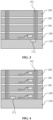
- FIG. 1 is a schematic structural diagram of a semiconductor device according to a first embodiment of the application.
- FIG. 2 is a circuit diagram of a temperature detection module in the semiconductor device of the application. Referring to FIG. 1 and FIG. 2 , the semiconductor device of the application comprises multiple memory chips 100 and a temperature detection module 110.
- the semiconductor device comprises a control chip 120, and the memory chips 100 and the temperature detection module 110 are electrically connected with the control chip 120.
- the control chip 120 is configured to control starting and running of the memory chips 100 and the temperature detection module 110.
- the starting of the memory chips 100 comprises powering on and self-detecting
- the running of the memory chips 100 comprises writing data into the memory chips 100, reading data from the memory chips 100 and deleting data accessible in the memory chips 100, etc.
- the function of the control chip 120 in terms of controlling the starting of the memory chips 100 and the like in the embodiments of the application may also be implemented by setting control circuits in the memory chips 100. In this cace, the control chip 120 may not be needed. It is understood by those of ordinary skill in the art that it can be set according to needs.
- the memory chip 100 is an existing memory into which the data can be written, from which the data can be read and/or from which the data can be deleted.
- the memory chip 100 is formed through a semiconductor integrated manufacturing process.
- the memory chip 100 may comprise a memory array and a peripheral circuit connected with the memory array.
- the memory array comprises multiple memory cells and bit lines, word lines and metal connecting lines (metal contact parts) connected with the memory cells.
- the memory cells are configured to store data, and the peripheral circuit is a related circuit when the memory array is operated.
- the memory chip 100 is a DRAM memory chip.
- the DRAM memory chip comprises multiple memory cells, each of the memory cells usually comprises a capacitor and a transistor. A grid electrode of the transistor is connected with a word line, a drain electrode of the transistor is connected with a bit line, and a source electrode of the transistor is connected with the capacitor.
- the memory chips 100 may be other types of memory chips.
- the temperature detection module 110 comprises multiple temperature detection units 111 and a processing unit 112.
- the multiple temperature detection units 111 are disposed on at least part of the memory chips 100 to detect temperatures of at least part of the memory chips 100 and output analog signals corresponding to the temperatures.
- the control chip 120 controls the memory chip 100 to start.
- the specific value of the set threshold may be set according to actual needs or experiences.
- the temperature detection units 111 are diodes.
- thermoelectric detection units 111 There may be a one-to-one correspondence or a one-to-many correspondence between the temperature detection units 111 and the memory chips 100.
- multiple temperature detection units 111 are provided and the number of the temperature detection units 111 is the same as the number of the memory chips 100, the temperature detection units 111 and the memory chips 100 have a one-to-one correspondence with each other. That is, one temperature detection unit 111 is disposed in one memory chip 100 and is configured to detect the temperature of the memory chip 100. Specifically, in the present embodiment, multiple memory chips 100 are provided, and multiple temperature detection units 111 are provided, as shown in FIG. 1. FIG. 1 schematically shows four memory chips 100 and four temperature detection units 111, the multiple memory chips 100 are stacked on each other, and the temperature detection units 111 correspond to the memory chips 100 one to one and are configured to detect the temperatures of the memory chips 100.
- the temperature detection units 111 and the memory chips 100 may possibly have both a one-to-one correspondence with each other and a one-to-many correspondence with each other, or only have a one-to-many correspondence with each other. That is, there may be a case where one temperature detection unit 111 only detects the temperature of one memory chip 100 and one temperature detection unit 111 detects the temperatures of multiple memory chips 100, or there may be only a case where one temperature detection unit 111 detects the temperatures of multiple memory chips 100.
- the temperature detection unit 111 may be formed in the memory chip 100 through a semiconductor integrated manufacturing process.
- the temperature detection unit 111 may be formed in the memory chip 100.
- the temperature detection units 111 correspond to the memory chips 100 one to one. That is, each of the memory chips 100 is disposed with one temperature detection unit 111.
- the temperature detection unit 111 may be formed in any one of the multiple memory chips 100 or formed in the middle or bottommost memory chip 100.
- FIG. 3 which is a schematic structural diagram of a semiconductor device according to the second embodiment of the application, the temperature detection unit 111 is disposed in the bottommost memory chip 100, and may measure the temperatures of four memory chips 100.
- the multiple temperature detection units 111 share the processing unit 112 with each other, and the processing unit 112 is configured to process a signal of at least one of the temperature detection units 111.
- the multiple temperature detection units 111 of the semiconductor device of the application share the processing unit 112 with each other, so that the occupied area of the temperature detection module is greatly reduced, and the effective area of the memory chips will not be affected.
- the processing unit 112 comprises multiple switches Sx, and the switches Sx are electrically connected with the temperature detection units 111 to select the temperature detection unit 111 with a signal needing to be processed by the processing unit 112. Specifically, when the switches are closed, the temperature detection units 111 are electrically connected with the processing unit 112, and when the switches are opened, the electrical connection between the temperature detection units 111 and the processing unit 112 is released.
- the temperature detection units 111 are diodes. Positive terminals of the diodes are electrically connected with the switches Sx, and negative terminals of the diodes are electrically connected with a grounding terminal VSS. The diode is sensitive to temperature. As the temperature of the ambient environment of the diode changes, the current of the diode changes, so that the temperature of the ambient environment may be measured.
- the switches Sx correspond to the temperature detection units 111 one to one. That is, one switch is electrically connected with one temperature detection unit 111 to realize an accurate control.
- the processing unit 112 accordingly comprises four switches S1 to S4.
- each of the four switches is electrically connected with one temperature detection unit 111 to control the electrical connection between the temperature detection unit 111 corresponding to the switch and the processing unit 112.
- the switch S1 when the electrical signal of the temperature detection unit 111 corresponding to the switch S1 needs to be processed, the switch S1 is closed, and the other switches are opened, so that the temperature detection unit 111 corresponding to the switch S1 is electrically connected with the processing unit 112 to realize processing of the signal.
- the switch S2 When the electrical signal of the temperature detection unit 111 corresponding to the switch S2 needs to be processed, the switch S2 is closed, and the other switches are opened, so that the temperature detection unit 111 corresponding to the switch S2 is electrically connected with the processing unit 112 to realize processing of the signal.
- the processing unit 112 further comprises a fixed resistor Ra and an A/D conversion module 1121.
- the fixed resistor Ra has a first terminal and a second terminal.
- the first terminal is electrically connected with the power source Vtemp, and the second terminal is electrically connected with the switches Sx.
- the A/D conversion module 1121 has an input terminal and an output terminal, the input terminal is electrically connected with the second terminal of the fixed resistor Ra, the output terminal is configured to output digital signals, and the A/D conversion module 1121 is configured to convert analog signals of the second terminal of the fixed resistor Ra into digital signals.
- the A/D conversion module 1121 comprises a resistor unit and multiple comparing units Px.
- the resistor unit has a first terminal and a second terminal.
- the first terminal of the resistor unit is electrically connected with a power source.
- the resistor unit and the temperature detection unit 111 may use the same power source, or may use different power sources.
- the first terminal of the resistor unit and the temperature detection unit 111 may use the same power source Vtemp; and when the A/D conversion module 1121 is disposed in the control chip 120, the first terminal of the resistor unit and the temperature detection unit 111 may use different power sources, in which the resistor unit may use a power source VDD.
- the second terminal of the resistor unit is electrically connected with the grounding terminal VSS.
- the resistor unit has multiple leading-out terminals Ax, and voltages of the leading-out terminals Ax are different from each other.
- the resistor unit comprises multiple sub-resistors Rx connected in series, and the numbers of the sub-resistors Rx between respective leading-out terminals Ax of the resistor unit and the second terminal of the resistor unit are different from each other, so that the voltages for the leading-out terminals Ax are different.
- a leading-out terminal A1 is spaced from the second terminal of the resistor unit by a sub-resistor R1
- a leading-out terminal A2 is spaced from the second terminal of the resistor unit by sub-resistors R1 and R2, so that the voltage of the leading-out terminal A1 and the voltage of the leading-out terminal A2 are different.
- the number of the sub-resistors Rx between respective leading-out terminals Ax of the resistor unit and the second terminal of the resistor unit is progressively increased by a preset numerical value.
- the preset numerical value may be a fixed value or a variable numerical value. Referring to FIG. 2 , in the present embodiment, the number of the sub-resistors Rx between respective leading-out terminals Ax of the resistor unit and the second terminal of the resistor unit is progressively increased by a fixed value of one. In other embodiments of the application, the number may also be progressively increased by a fixed value of two and the like.
- the preset numerical value is a variable numerical value, the preset numerical value has a changing trend.
- the changing trend is set according to a voltage increase amplitude of the leading-out terminal Ax. For example, when the voltage increase amplitude of the leading-out terminal Ax is increasing, the changing trend of the preset numerical value is increasing; when the voltage increase amplitude of the leading-out terminal Ax is decreasing, the changing trend of the preset value is decreasing; and when the voltage increase amplitude of the leading-out terminal Ax is first increasing and then decreasing, the changing trend of the preset numerical value is first increasing and then decreasing.
- the resistance values of the sub-resistors Rx are the same or different, so that the voltage increase amplitude changes between the leading-out terminals Ax are consistent or inconsistent with each other.
- the pattern layout difficulty may be reduced, and the pattern layout is simple and easy to implement, which facilitates manufacturing.
- Signals of the input terminal of the A/D conversion module serve as input signals of the comparing units Px. That is, analog signals output by the temperature detection units serve as input signals of the comparing units Px. Signals of the multiple leading-out terminals Ax of the resistor unit respectively serve as reference signals of the multiple comparing units Px.
- the leading-out terminals Ax correspond to the comparing units Px one to one. For example, a signal of the leading-out terminal A1 serves as a reference signal of the comparing unit P1, a signal of the leading-out terminal A2 serves as a reference signal of the comparing unit P2.
- the leading-out terminals Ax correspond to the comparing units Px one to one.
- the comparing units Px output digital signals. According to the digital signals output by the comparing units Px, the temperature of the memory chip 100, detected by the temperature detection unit 111, may be obtained.
- the voltages of the leading-out terminals Ax are changed unevenly, to cause the reference signals of the multiple comparing units Px to be changed unevenly, so that in different voltage regions, the increase amplitudes of the reference signals of the comparing units Px are different, and thus the measurement accuracy of the voltage regions can be changed.
- the preset numerical value is changed in a small amplitude, to cause the increase amplitude of the reference signal to be small.
- the number of signal sampling points can be increased, and then the measurement accuracy of this region can be improved.
- the preset numerical value is changed in a large amplitude, to cause the increase amplitude of the reference signal to be large. In this case, the number of signal sampling points can be reduced, and then the measurement efficiency can be improved.
- the increase amplitude of the preset numerical value is small, for example, the increase amplitude of the preset numerical value is 1, so that the increase amplitude of the reference signal is 0.1 V
- the number of sampling points in this voltage region may be increased, and thus the measurement accuracy can be improved.
- the increase amplitude of the preset numerical value is large, for example, the increase amplitude of the preset value is 3, so that the increase amplitude of the reference signal is 0.3 V In this case, by appropriately reducing the number of sampling points, the measurement efficiency can be improved.
- the A/D conversion module 1121 comprises an output unit 1122.
- the output unit 1122 is connected with the comparing units Px and is configured to output the digital signals.
- the A/D conversion module 1121 comprises an encoding unit EEC.
- the encoding unit EEC receives and encodes the digital signals output by the comparing units Px, the formed signals are input into the output unit 1120, and the output unit 1122 outputs the encoded digital signals.
- the processing unit 112 further comprises an adjustable resistance unit Rb configured to calibrate the temperature detection unit 111.
- the adjustable resistance unit 111 has a first terminal and a second terminal. The first terminal of the adjustable resistance unit Rb is electrically connected with the grounding terminal VSS, and the second terminal of the adjustable resistance unit Rb is electrically connected with the second terminal of the fixed resistor Ra.
- the resistance value of the adjustable resistance unit Rb may be changed. For example, the resistance value of the adjustable resistance unit Rb may be changed through the control of the control chip 120, to adjust the voltage of the output terminal of the temperature detection unit 111, thereby realizing the calibration of the temperature detection unit 111.
- one end of the switch Sx is electrically connected with the temperature detection units 111, and another end of the switch is connected with the adjustable resistance unit Rb. That is, the temperature detection units 111 and the adjustable resistance unit Rb are respectively connected to two ends of the switch Sx.
- both the adjustable resistance unit Rb and the temperature detection units 111 are connected to the same end of the switch Sx. That is, both the adjustable resistance unit Rb and the temperature detection units 111 are electrically connected with one end or another end of the switch Sx.
- the processing unit 112 is disposed on the control chip 120 or disposed on one of the memory chips 100. In the present embodiment, referring to FIG. 1 , the processing unit 112 is disposed on the control chip 120. In other embodiments of the application, the processing unit 112 is disposed on one of the memory chips 100.
- FIG. 4 is a schematic structural diagram of a semiconductor device according to a third embodiment of the application. In the third embodiment, the processing unit 112 is disposed on the bottommost memory chip 100.
- FIG. 5 is a schematic diagram of electrical connection of the semiconductor device according to the invention.
- the temperature detection unit 111 is powered by a power source Vtemp
- the memory chip 100 is powered by a power source VDD.
- the grounding terminal VSS, the power source VDD and the power source Vtemp are provided by the control chip 120. Since the temperature detection unit 111 and the memory chip 100 are powered by different power sources, the power supply of the temperature detection unit 111 and the power supply of the memory cell 100 may be independently controlled, so as to realize the starting of the temperature detection unit 111 and of the memory chip 100 at different times.
- the starting of the temperature detection unit 111 and the starting of the memory chip 100 may be controlled respectively. That is, the starting of the temperature detection unit 111 is not affected by whether the memory chip 100 is started or not, and thus the detection of the temperature of the memory chip 100 is not affected by whether the memory chip 100 is started or not, so as to provide a reference for starting and running of the memory chip 100, thereby preventing the memory chip 100 from starting or running at a low temperature, and improving the stability of the memory chip 100.
- the temperature has a great influence on the performance of the memory chip 100, especially when the memory chip 100 is started.
- the time for writing data into the memory chip 100 will change (such as increase), which will affect the writing stability of the memory chip 100.
- the temperature of the memory chip needs to be measured before the memory chip 100 is started, so that the memory chip 100 may be started within a suitable temperature.
- the power supply of the temperature detection unit 111 is earlier than the power supply of the memory chip 100. That is, the temperature detection unit 111 has been started before the memory chip 100 is started, so that a temperature of the memory chip before the memory chip 100 is started may be obtained to provide a reference for starting of the memory chip 100.
- a power supply time difference between the temperature detection unit 111 and the memory chip 100 depends on a temperature change rate of the memory chip 100. When the temperature change rate of the memory chip 100 is large and the time for the memory chip 100 to reach the preset temperature is short, the power supply time difference between the temperature detection unit 111 and the memory chip 100 is small. When the temperature change rate of the memory chip 100 is small and the time for the memory chip 100 to reach the preset temperature is long, the power supply time difference between the temperature detection unit 111 and the memory chip 100 is large.
- the temperature detection unit 111 shares the same grounding terminal VSS with the memory chip 100, which has the advantages that on one hand, the leakage current of the memory chip 100 in a non-starting stage may not be increased, and on the other hand, the number of pins may be reduced to save the space.
- a Through-Silicon-Via (TSV) interconnect structure 101 is formed in the memory chip 100.
- the memory chip 100 is electrically connected with the control chip 120 through the TSV interconnect structure 101 and the temperature detection unit 111 is electrically connected with the processing unit 112 through the TSV interconnect structure 101.
- the memory chip 100 is electrically connected with the grounding terminal VSS and the power source VDD through the TSV interconnect structure 101 and the temperature detection unit 111 is electrically connected with the power source Vtemp and the grounding terminal VSS through the TSV interconnect structure 101.
- the respective memory chips 100 may be connected with the control chip 120 through different TSV interconnect structures.
- TSV interconnect structures there may be a case where respective temperature detection units 111 are connected with the processing unit 112 through different TSV interconnect structures, and there may also be a case where the multiple temperature detection units 111 are connected with the processing unit 112 through a same TSV interconnect structure.
- the memory chip 100 and the temperature detection unit 111 are connected with power sources through different TSV interconnect structures, so that the temperature detection unit 111 and the memory chip 100 are be powered by different power sources. Further, the power supply of the multiple temperature detection units 111 may also share the same TSV interconnect structure.
- the memory chip 100 and the temperature detection unit 111 may also be electrically connected with the control chip 120 and the processing unit 112 through metal leads (formed by a lead bonding process).
- the semiconductor device further comprises a circuit substrate 130, in which a connecting line (not shown in the figure) is provided.
- a connecting line not shown in the figure
- both the memory chip 100 and the control chip 120 are located on the circuit substrate 130, and the memory chip 100 is connected with the control chip 120 through the connecting line in the circuit substrate 130.
- the temperature detection unit 111 is disposed in the memory chip 100
- the processing unit 112 is disposed in the control chip 120.
- the circuit substrate 130 comprises, but is not limited to, a Printed Circuit Board (PCB).
- the semiconductor device of the application uses the temperature detection module to detect the temperatures of the memory chips.
- the temperature detected by the temperature detection module reaches the set threshold, or after the temperature of the memory chip 100 reaches the set threshold, the memory chip is started.
- the temperature detected by the temperature detection module provides a reference for starting and running of the memory chip, thereby preventing the memory chip from starting and running at a low temperature, shortening the writing time, and improving the writing stability of the memory chip.
- the control chip 120 of the application may also be started before the memory chip 100 is started, and the control chip 120 uses the heat generated by itself after starting, to heat the memory chip 100, so as to quickly increase the temperature of the memory chip 100.
- control chip 120 controls the temperature detection unit 111 to start, so as to detect the temperature of the memory chip 100.
- the temperature detection unit 111 may also transmit the detected temperature to the control chip 120 to serve as data of the control chip 120.
- the control chip 120 may determine whether the temperature detected by the temperature detection unit 111 reaches a set threshold, and when the temperature detected by the temperature detection unit 111 reaches the set threshold, the control chip 120 controls the memory chip 100 to start.
- the control unit 120 in response to determining that the temperature detected by the temperature detection unit 111 reaches the set threshold, first controls the memory chip 100 closest to the control chip 120 to start, and then controls the other memory chips 100 above the memory chip 100 closest to the control chip to start sequentially.
- the control unit 120 in responsive to determining that the temperature detected by a certain temperature detection unit 111 reaches the set threshold, controls the memory chip 100 corresponding to the temperature detection unit 111 to start.
- the stack as shown in FIG. 1 comprises four memory chips 100, and each of the memory chips 100 is correspondingly provided with one temperature detection unit 111, so that each temperature detection unit 111 detects the temperature of the corresponding memory chip 100 to obtain four temperature detection values.
- the control chip 120 sequentially determines whether the temperatures detected by the four temperature detection units 111 reach the set threshold.
- the control chip 120 controls the memory chip corresponding to the temperature detection unit 111 to start. For example, when the temperature detected by the temperature detection unit 111 in the bottommost memory chip 100 in the stack first reaches the set threshold, the control chip 120 first controls the bottommost memory chip 100 in the stack to start. Subsequently, when the temperature detected by the temperature detection unit 111 corresponding to a second memory chip 100 from the bottommost memory chip in the stack also reaches the set threshold, a control unit 301 controls the second memory chip 100 from the bottommost memory chip in the stack to start.
- the starting of the memory chips 100 in the upper two layers may be implemented by analogy.
- control structure and control mode may further improve the accuracy of the start timing of each of the memory chips 100, and may further shorten the writing time for writing data into each of the memory chips 100 in a low-temperature environment, thereby further improving the writing stability of each of the memory chips 100.
- the temperature of the memory chip 100 may rise to the set threshold through the control chip 120, so as to prevent bit lines, word lines and metal connecting lines (metal contact parts) in the memory chip 100 from increasing in resistance due to too low ambient temperature, thereby shortening the writing time for writing data into the memory chip in a low-temperature environment, and improving the writing stability of the memory chip.
- the set threshold may be set in the control chip 120, and the specific value of the set threshold may be set according to actual needs or experiences.
- control chip 120 may be provided with an additional heating circuit (not shown in the figures).
- the heating circuit is configured to heat the memory chip 100. Before or after the control chip 120 heats the memory chip 100, the control chip 120 determines whether the temperature of the memory chip 100, detected by the temperature detection unit 111, reaches the set threshold or not. When the temperature does not reach the set threshold, the control chip 120 controls the heating circuit to heat the memory chip 100. When the temperature reaches the set threshold, the control chip 120 controls the heating circuit to stop heating the memory chip 100.
Landscapes
- Engineering & Computer Science (AREA)
- Microelectronics & Electronic Packaging (AREA)
- Computer Hardware Design (AREA)
- Physics & Mathematics (AREA)
- General Physics & Mathematics (AREA)
- Power Engineering (AREA)
- Semiconductor Integrated Circuits (AREA)
- Dram (AREA)
Claims (14)
- Dispositif semi-conducteur, dans lequel le dispositif semi-conducteur comprend une pluralité de puces de mémoire (100) et un module de détection de température (110), dans lequel le module de détection de température comprend :une pluralité d'unités de détection de température (111) disposées sur au moins une partie des puces mémoire pour détecter les températures d'au moins une partie des puces mémoire ; etune unité de traitement (112), dans lequel la pluralité d'unités de détection de température (111) partagent l'unité de traitement (112) les unes avec les autres, et l'unité de traitement (112) est configurée pour traiter un signal d'au moins l'une des unités de détection de température unités (111),caractérisé en ce qu'une alimentation électrique des unités de détection de température (111) et une alimentation électrique des puces de mémoire (100) sont réalisées par des sources d'alimentation différentes et contrôlables indépendamment (Vtemp, VDD) et l'alimentation électrique des unités de détection de température (111) est démarrée avant l'alimentation des puces mémoire (100).
- Dispositif semi-conducteur selon la revendication 1, caractérisé en ce que l'unité de traitement (112) comprend une pluralité de commutateurs, et les commutateurs sont connectés électriquement aux unités de détection de température (111) pour sélectionner l'unité de détection de température avec un signal devant être traité par l'unité de traitement (112).
- Dispositif semi-conducteur selon la revendication 2, caractérisé en ce que l'unité de traitement (112) comprend une résistance fixe (Ra), et dans lequel la résistance fixe a une première borne reliée électriquement à la source d'alimentation des unités de détection de température (Vtemp) et une deuxième borne connectée aux commutateurs.
- Dispositif semi-conducteur selon la revendication 3, caractérisé en ce que l'unité de traitement (112) comprend en outre un module de conversion analogique/numérique, A/N (1121), et dans lequel le module de conversion A/N a une borne d'entrée connectée électriquement à la deuxième borne de la résistance fixe (Ra) et une borne de sortie configurée pour émettre des signaux numériques, et le module de conversion A/N (1121) est configuré pour convertir des signaux analogiques de la deuxième borne de la résistance fixe (Ra) en signaux numériques.
- Dispositif semi-conducteur selon la revendication 4, caractérisé en ce que le module de conversion A/N (1121) comprend :une unité de résistance, dans lequel l'unité de résistance a une première borne connectée électriquement à la source d'alimentation et une deuxième borne connectée électriquement à une borne de mise à la masse (VSS), et l'unité de résistance a une pluralité de bornes de sortie, les tensions des bornes de sortie étant différentes les unes des autres; etune pluralité d'unités de comparaison, dans lequel les signaux de la borne d'entrée du module de conversion A/N servent de signaux d'entrée des unités de comparaison, les signaux de la pluralité de bornes de sortie de l'unité de résistance servent respectivement de signaux de référence de la pluralité de unités de comparaison, et les unités de comparaison délivrent des signaux numériques
- Dispositif semi-conducteur selon la revendication 5, caractérisé en ce que l'unité de résistance comprend une pluralité de sous-résistances connectées en série, et les nombres des sous-résistances entre les bornes de sortie respectives de l'unité de résistance et la deuxième borne de l'unité de résistance sont différents les uns des autres, de sorte que les tensions des bornes de sortie respectives sont différentes les unes des autres.
- Dispositif semi-conducteur selon la revendication 6, caractérisé en ce que les valeurs de résistance des sous-résistances sont identiques ou différentes.
- Dispositif semi-conducteur selon la revendication 3, caractérisé en ce que les unités de détection de température (111) sont des diodes, et les bornes positives des diodes sont reliées électriquement aux interrupteurs et les bornes négatives des diodes sont reliées électriquement à une borne de masse (VSS).
- Dispositif semi-conducteur selon la revendication 8, caractérisé en ce que l'unité de traitement (112) comprend en outre une unité à résistance réglable (Rb), et l'unité à résistance réglable (Rb) a une première borne reliée électriquement à la borne de masse (V SS) et une deuxième borne connectée électriquement à la deuxième borne de la résistance fixe (Ra).
- Dispositif semi-conducteur selon la revendication 1, caractérisé en ce que le dispositif semi-conducteur comprend en outre une puce de commande (120), et les puces de mémoire (100) et le module de détection de température (110) sont connectés électriquement à la puce de commande (120).
- Dispositif semiconducteur selon la revendication 10, caractérisé en ce que l'unité de traitement (112) est disposée sur la puce de commande (120) ou disposée sur l'une des puces mémoire (100).
- Dispositif semi-conducteur selon la revendication 10, caractérisé en ce que la pluralité de puces mémoire (100) sont séquentiellement empilées vers le haut sur la puce de commande (120).
- Dispositif semi-conducteur selon la revendication 10, caractérisé en ce que le dispositif semi-conducteur comprend en outre un substrat de circuit (130), une ligne de connexion est prévue dans le substrat de circuit (130), à la fois la puce mémoire (100) et la puce de commande (120) sont situés sur le substrat de circuit (130), et la puce de mémoire (100) est connectée à la puce de commande (120) par l'intermédiaire de la ligne de connexion dans le substrat de circuit.
- Dispositif semi-conducteur selon la revendication 10, caractérisé en ce que la puce de commande (120) est configurée pour chauffer la puce mémoire (100) avant le démarrage de la puce mémoire et pour déterminer si la température détectée par l'unité de détection de température (111) atteint un seuil défini, et dans lequel la puce de commande (120) est configurée pour commander le démarrage de la puce de mémoire (100), lorsque la température détectée par l'unité de détection de température (111) atteint le seuil défini.
Applications Claiming Priority (2)
| Application Number | Priority Date | Filing Date | Title |
|---|---|---|---|
| CN202010689669.1A CN113948117B (zh) | 2020-07-17 | 2020-07-17 | 半导体装置 |
| PCT/CN2020/136390 WO2022011955A1 (fr) | 2020-07-17 | 2020-12-15 | Dispositif à semi-conducteur |
Publications (3)
| Publication Number | Publication Date |
|---|---|
| EP3968324A1 EP3968324A1 (fr) | 2022-03-16 |
| EP3968324A4 EP3968324A4 (fr) | 2022-07-13 |
| EP3968324B1 true EP3968324B1 (fr) | 2023-07-05 |
Family
ID=79292685
Family Applications (1)
| Application Number | Title | Priority Date | Filing Date |
|---|---|---|---|
| EP20937168.1A Active EP3968324B1 (fr) | 2020-07-17 | 2020-12-15 | Dispositif à semi-conducteur |
Country Status (2)
| Country | Link |
|---|---|
| US (1) | US11462257B2 (fr) |
| EP (1) | EP3968324B1 (fr) |
Family Cites Families (38)
| Publication number | Priority date | Publication date | Assignee | Title |
|---|---|---|---|---|
| KR100541824B1 (ko) | 2003-10-06 | 2006-01-10 | 삼성전자주식회사 | 반도체 집적회로에 채용하기 적합한 온도감지 회로 |
| US7266031B2 (en) * | 2003-11-19 | 2007-09-04 | Infineon Technologies Ag | Internal voltage generator with temperature control |
| KR100577560B1 (ko) | 2003-12-23 | 2006-05-08 | 삼성전자주식회사 | 온도감지 데이터에 응답하는 내부회로를 갖는 반도체메모리장치 |
| US7356426B2 (en) * | 2004-09-30 | 2008-04-08 | Intel Corporation | Calibration of thermal sensors for semiconductor dies |
| US20060290366A1 (en) * | 2005-06-28 | 2006-12-28 | Intel Corporation | Monitoring multiple electronic devices under test |
| KR101224919B1 (ko) | 2006-02-07 | 2013-01-22 | 삼성전자주식회사 | 온도 변화에 따라 고전압 발생 회로의 출력 전압 레벨을조절하는 반도체 메모리 장치 |
| US7383149B1 (en) | 2006-04-19 | 2008-06-03 | Darryl Walker | Semiconductor device having variable parameter selection based on temperature and test method |
| US7480588B1 (en) | 2006-04-19 | 2009-01-20 | Darryl Walker | Semiconductor device having variable parameter selection based on temperature and test method |
| DE102006018921A1 (de) | 2006-04-24 | 2007-11-08 | Infineon Technologies Ag | Integrierter Halbleiterspeicher mit Auffrischung von Speicherzellen |
| KR100851989B1 (ko) | 2006-10-12 | 2008-08-13 | 주식회사 하이닉스반도체 | 반도체 메모리 장치의 온도정보 출력회로 및 방법 |
| KR20090032705A (ko) * | 2007-09-28 | 2009-04-01 | 삼성전자주식회사 | 온도 변화에 적응적인 클럭을 이용하는 저장장치 및 이를이용한 방송수신장치 |
| KR101132795B1 (ko) | 2010-02-25 | 2012-04-02 | 주식회사 하이닉스반도체 | 온도센서 |
| KR101817156B1 (ko) | 2010-12-28 | 2018-01-10 | 삼성전자 주식회사 | 관통 전극을 갖는 적층 구조의 반도체 장치, 반도체 메모리 장치, 반도체 메모리 시스템 및 그 동작방법 |
| JP5786571B2 (ja) * | 2011-09-07 | 2015-09-30 | 富士電機株式会社 | パワー半導体装置の温度測定装置 |
| KR102098248B1 (ko) | 2013-06-03 | 2020-04-07 | 삼성전자 주식회사 | 온도에 따라 완화된 타이밍 요건으로 사용되는 메모리 장치 및 이를 이용하는 메모리 콘트롤러 |
| US20150043266A1 (en) * | 2013-08-09 | 2015-02-12 | Samsung Electronics Co., Ltd. | Enhanced temperature range for resistive type memory circuits with pre-heat operation |
| WO2015025422A1 (fr) | 2013-08-23 | 2015-02-26 | 三菱電機株式会社 | Dispositif à semi-conducteurs |
| KR20150052631A (ko) | 2013-11-06 | 2015-05-14 | 에스케이하이닉스 주식회사 | 반도체 장치 및 반도체 시스템 |
| US9194754B2 (en) | 2014-03-28 | 2015-11-24 | Darryl G. Walker | Power up of semiconductor device having a temperature circuit and method therefor |
| JP2016046617A (ja) | 2014-08-21 | 2016-04-04 | ルネサスエレクトロニクス株式会社 | 半導体装置 |
| KR20160056056A (ko) * | 2014-11-11 | 2016-05-19 | 삼성전자주식회사 | 반도체 메모리 장치 및 이를 포함하는 메모리 시스템 |
| CN104807561B (zh) | 2015-04-29 | 2017-11-28 | 清华大学深圳研究生院 | 电阻型温度传感芯片的校准电路和校准方法 |
| US9520189B1 (en) | 2015-10-29 | 2016-12-13 | International Business Machines Corporation | Enhanced temperature compensation for resistive memory cell circuits |
| US9927986B2 (en) | 2016-02-26 | 2018-03-27 | Sandisk Technologies Llc | Data storage device with temperature sensor and temperature calibration circuitry and method of operating same |
| US10564900B2 (en) | 2016-03-04 | 2020-02-18 | Western Digital Technologies, Inc. | Temperature variation compensation |
| JP6756965B2 (ja) | 2016-12-09 | 2020-09-16 | 富士通株式会社 | 半導体装置及び半導体装置の制御方法 |
| CN108447511B (zh) | 2017-08-21 | 2021-03-23 | 长鑫存储技术有限公司 | 半导体存储器及其控制方法 |
| KR20190036893A (ko) * | 2017-09-28 | 2019-04-05 | 삼성전자주식회사 | 메모리 장치 및 그것의 제어 방법 |
| JP2019168755A (ja) | 2018-03-22 | 2019-10-03 | 東芝メモリ株式会社 | メモリシステム、電源制御回路及び制御方法 |
| EP3700004A4 (fr) * | 2018-06-14 | 2021-03-10 | Lg Chem, Ltd. | Appareil et procédé de mesure de la température de batterie |
| CN208953151U (zh) | 2018-10-18 | 2019-06-07 | 杭州士兰微电子股份有限公司 | 过温检测装置 |
| JP2020077443A (ja) | 2018-11-05 | 2020-05-21 | キオクシア株式会社 | メモリシステム |
| WO2020101705A1 (fr) * | 2018-11-16 | 2020-05-22 | Hewlett-Packard Development Company, L.P. | Détection de température |
| CN113748598B (zh) | 2019-04-04 | 2024-04-26 | 株式会社村田制作所 | 放大电路以及放大装置 |
| JP6818919B1 (ja) | 2020-02-06 | 2021-01-27 | 三菱電機株式会社 | 温度センサモジュール |
| CN212303077U (zh) | 2020-07-17 | 2021-01-05 | 长鑫存储技术有限公司 | 半导体装置 |
| CN212303078U (zh) | 2020-07-17 | 2021-01-05 | 长鑫存储技术有限公司 | 半导体装置 |
| CN212303079U (zh) | 2020-07-17 | 2021-01-05 | 长鑫存储技术有限公司 | 半导体装置 |
-
2020
- 2020-12-15 EP EP20937168.1A patent/EP3968324B1/fr active Active
-
2021
- 2021-07-30 US US17/389,618 patent/US11462257B2/en active Active
Also Published As
| Publication number | Publication date |
|---|---|
| US20220020426A1 (en) | 2022-01-20 |
| EP3968324A4 (fr) | 2022-07-13 |
| US11462257B2 (en) | 2022-10-04 |
| EP3968324A1 (fr) | 2022-03-16 |
Similar Documents
| Publication | Publication Date | Title |
|---|---|---|
| CN212303078U (zh) | 半导体装置 | |
| CN212303077U (zh) | 半导体装置 | |
| CN212303079U (zh) | 半导体装置 | |
| US6798706B2 (en) | Integrated circuit with temperature sensor and method for heating the circuit | |
| US12111214B2 (en) | Semiconductor device | |
| EP3968324B1 (fr) | Dispositif à semi-conducteur | |
| EP4024396B1 (fr) | Procédé de lecture/écriture destiné à un dispositif de stockage, et dispositif de stockage | |
| EP4095857B1 (fr) | Appareil à semi-conducteur | |
| CN113870916B (zh) | 半导体装置 | |
| EP3965105B1 (fr) | Étalonnage d'un module de détection de température dans une mémoire semi-conductrice comprenant plusieurs puces de mémoire | |
| CN113870917B (zh) | 半导体装置 | |
| CN113948117B (zh) | 半导体装置 | |
| EP3961633B1 (fr) | Dispositif à semi-conducteur | |
| CN113948118A (zh) | 半导体装置 | |
| JP7352750B2 (ja) | 半導体装置 | |
| CN113948119A (zh) | 半导体装置 | |
| CN114141287B (zh) | 存储装置的读写方法及存储装置 |
Legal Events
| Date | Code | Title | Description |
|---|---|---|---|
| STAA | Information on the status of an ep patent application or granted ep patent |
Free format text: STATUS: UNKNOWN |
|
| STAA | Information on the status of an ep patent application or granted ep patent |
Free format text: STATUS: THE INTERNATIONAL PUBLICATION HAS BEEN MADE |
|
| PUAI | Public reference made under article 153(3) epc to a published international application that has entered the european phase |
Free format text: ORIGINAL CODE: 0009012 |
|
| STAA | Information on the status of an ep patent application or granted ep patent |
Free format text: STATUS: REQUEST FOR EXAMINATION WAS MADE |
|
| 17P | Request for examination filed |
Effective date: 20211129 |
|
| AK | Designated contracting states |
Kind code of ref document: A1 Designated state(s): AL AT BE BG CH CY CZ DE DK EE ES FI FR GB GR HR HU IE IS IT LI LT LU LV MC MK MT NL NO PL PT RO RS SE SI SK SM TR |
|
| A4 | Supplementary search report drawn up and despatched |
Effective date: 20220613 |
|
| RIC1 | Information provided on ipc code assigned before grant |
Ipc: H01L 25/18 20060101ALN20220608BHEP Ipc: G11C 11/4074 20060101ALN20220608BHEP Ipc: G11C 29/02 20060101ALI20220608BHEP Ipc: G11C 7/20 20060101ALI20220608BHEP Ipc: G11C 5/14 20060101ALI20220608BHEP Ipc: G11C 5/04 20060101ALI20220608BHEP Ipc: G11C 5/02 20060101ALI20220608BHEP Ipc: G11C 7/04 20060101AFI20220608BHEP |
|
| RIC1 | Information provided on ipc code assigned before grant |
Ipc: H01L 25/18 20060101ALN20230204BHEP Ipc: G11C 11/4074 20060101ALN20230204BHEP Ipc: G01K 1/02 20060101ALI20230204BHEP Ipc: G11C 29/02 20060101ALI20230204BHEP Ipc: G11C 7/20 20060101ALI20230204BHEP Ipc: G11C 5/14 20060101ALI20230204BHEP Ipc: G11C 5/04 20060101ALI20230204BHEP Ipc: G11C 5/02 20060101ALI20230204BHEP Ipc: G11C 7/04 20060101AFI20230204BHEP |
|
| RIC1 | Information provided on ipc code assigned before grant |
Ipc: H01L 25/18 20060101ALN20230307BHEP Ipc: G11C 11/4074 20060101ALN20230307BHEP Ipc: G01K 1/02 20060101ALI20230307BHEP Ipc: G11C 29/02 20060101ALI20230307BHEP Ipc: G11C 7/20 20060101ALI20230307BHEP Ipc: G11C 5/14 20060101ALI20230307BHEP Ipc: G11C 5/04 20060101ALI20230307BHEP Ipc: G11C 5/02 20060101ALI20230307BHEP Ipc: G11C 7/04 20060101AFI20230307BHEP |
|
| GRAP | Despatch of communication of intention to grant a patent |
Free format text: ORIGINAL CODE: EPIDOSNIGR1 |
|
| STAA | Information on the status of an ep patent application or granted ep patent |
Free format text: STATUS: GRANT OF PATENT IS INTENDED |
|
| DAV | Request for validation of the european patent (deleted) | ||
| DAX | Request for extension of the european patent (deleted) | ||
| INTG | Intention to grant announced |
Effective date: 20230417 |
|
| GRAS | Grant fee paid |
Free format text: ORIGINAL CODE: EPIDOSNIGR3 |
|
| GRAA | (expected) grant |
Free format text: ORIGINAL CODE: 0009210 |
|
| STAA | Information on the status of an ep patent application or granted ep patent |
Free format text: STATUS: THE PATENT HAS BEEN GRANTED |
|
| AK | Designated contracting states |
Kind code of ref document: B1 Designated state(s): AL AT BE BG CH CY CZ DE DK EE ES FI FR GB GR HR HU IE IS IT LI LT LU LV MC MK MT NL NO PL PT RO RS SE SI SK SM TR |
|
| P01 | Opt-out of the competence of the unified patent court (upc) registered |
Effective date: 20230530 |
|
| REG | Reference to a national code |
Ref country code: CH Ref legal event code: EP |
|
| REG | Reference to a national code |
Ref country code: AT Ref legal event code: REF Ref document number: 1585584 Country of ref document: AT Kind code of ref document: T Effective date: 20230715 |
|
| REG | Reference to a national code |
Ref country code: DE Ref legal event code: R096 Ref document number: 602020013470 Country of ref document: DE |
|
| REG | Reference to a national code |
Ref country code: IE Ref legal event code: FG4D |
|
| REG | Reference to a national code |
Ref country code: LT Ref legal event code: MG9D |
|
| REG | Reference to a national code |
Ref country code: NL Ref legal event code: MP Effective date: 20230705 |
|
| REG | Reference to a national code |
Ref country code: AT Ref legal event code: MK05 Ref document number: 1585584 Country of ref document: AT Kind code of ref document: T Effective date: 20230705 |
|
| PG25 | Lapsed in a contracting state [announced via postgrant information from national office to epo] |
Ref country code: NL Free format text: LAPSE BECAUSE OF FAILURE TO SUBMIT A TRANSLATION OF THE DESCRIPTION OR TO PAY THE FEE WITHIN THE PRESCRIBED TIME-LIMIT Effective date: 20230705 |
|
| PG25 | Lapsed in a contracting state [announced via postgrant information from national office to epo] |
Ref country code: GR Free format text: LAPSE BECAUSE OF FAILURE TO SUBMIT A TRANSLATION OF THE DESCRIPTION OR TO PAY THE FEE WITHIN THE PRESCRIBED TIME-LIMIT Effective date: 20231006 |
|
| PG25 | Lapsed in a contracting state [announced via postgrant information from national office to epo] |
Ref country code: ES Free format text: LAPSE BECAUSE OF FAILURE TO SUBMIT A TRANSLATION OF THE DESCRIPTION OR TO PAY THE FEE WITHIN THE PRESCRIBED TIME-LIMIT Effective date: 20230705 |
|
| PG25 | Lapsed in a contracting state [announced via postgrant information from national office to epo] |
Ref country code: IS Free format text: LAPSE BECAUSE OF FAILURE TO SUBMIT A TRANSLATION OF THE DESCRIPTION OR TO PAY THE FEE WITHIN THE PRESCRIBED TIME-LIMIT Effective date: 20231105 |
|
| PG25 | Lapsed in a contracting state [announced via postgrant information from national office to epo] |
Ref country code: SE Free format text: LAPSE BECAUSE OF FAILURE TO SUBMIT A TRANSLATION OF THE DESCRIPTION OR TO PAY THE FEE WITHIN THE PRESCRIBED TIME-LIMIT Effective date: 20230705 Ref country code: RS Free format text: LAPSE BECAUSE OF FAILURE TO SUBMIT A TRANSLATION OF THE DESCRIPTION OR TO PAY THE FEE WITHIN THE PRESCRIBED TIME-LIMIT Effective date: 20230705 Ref country code: PT Free format text: LAPSE BECAUSE OF FAILURE TO SUBMIT A TRANSLATION OF THE DESCRIPTION OR TO PAY THE FEE WITHIN THE PRESCRIBED TIME-LIMIT Effective date: 20231106 Ref country code: NO Free format text: LAPSE BECAUSE OF FAILURE TO SUBMIT A TRANSLATION OF THE DESCRIPTION OR TO PAY THE FEE WITHIN THE PRESCRIBED TIME-LIMIT Effective date: 20231005 Ref country code: LV Free format text: LAPSE BECAUSE OF FAILURE TO SUBMIT A TRANSLATION OF THE DESCRIPTION OR TO PAY THE FEE WITHIN THE PRESCRIBED TIME-LIMIT Effective date: 20230705 Ref country code: LT Free format text: LAPSE BECAUSE OF FAILURE TO SUBMIT A TRANSLATION OF THE DESCRIPTION OR TO PAY THE FEE WITHIN THE PRESCRIBED TIME-LIMIT Effective date: 20230705 Ref country code: IS Free format text: LAPSE BECAUSE OF FAILURE TO SUBMIT A TRANSLATION OF THE DESCRIPTION OR TO PAY THE FEE WITHIN THE PRESCRIBED TIME-LIMIT Effective date: 20231105 Ref country code: HR Free format text: LAPSE BECAUSE OF FAILURE TO SUBMIT A TRANSLATION OF THE DESCRIPTION OR TO PAY THE FEE WITHIN THE PRESCRIBED TIME-LIMIT Effective date: 20230705 Ref country code: GR Free format text: LAPSE BECAUSE OF FAILURE TO SUBMIT A TRANSLATION OF THE DESCRIPTION OR TO PAY THE FEE WITHIN THE PRESCRIBED TIME-LIMIT Effective date: 20231006 Ref country code: FI Free format text: LAPSE BECAUSE OF FAILURE TO SUBMIT A TRANSLATION OF THE DESCRIPTION OR TO PAY THE FEE WITHIN THE PRESCRIBED TIME-LIMIT Effective date: 20230705 Ref country code: ES Free format text: LAPSE BECAUSE OF FAILURE TO SUBMIT A TRANSLATION OF THE DESCRIPTION OR TO PAY THE FEE WITHIN THE PRESCRIBED TIME-LIMIT Effective date: 20230705 Ref country code: AT Free format text: LAPSE BECAUSE OF FAILURE TO SUBMIT A TRANSLATION OF THE DESCRIPTION OR TO PAY THE FEE WITHIN THE PRESCRIBED TIME-LIMIT Effective date: 20230705 |
|
| PG25 | Lapsed in a contracting state [announced via postgrant information from national office to epo] |
Ref country code: PL Free format text: LAPSE BECAUSE OF FAILURE TO SUBMIT A TRANSLATION OF THE DESCRIPTION OR TO PAY THE FEE WITHIN THE PRESCRIBED TIME-LIMIT Effective date: 20230705 |
|
| REG | Reference to a national code |
Ref country code: DE Ref legal event code: R097 Ref document number: 602020013470 Country of ref document: DE |
|
| PG25 | Lapsed in a contracting state [announced via postgrant information from national office to epo] |
Ref country code: SM Free format text: LAPSE BECAUSE OF FAILURE TO SUBMIT A TRANSLATION OF THE DESCRIPTION OR TO PAY THE FEE WITHIN THE PRESCRIBED TIME-LIMIT Effective date: 20230705 Ref country code: RO Free format text: LAPSE BECAUSE OF FAILURE TO SUBMIT A TRANSLATION OF THE DESCRIPTION OR TO PAY THE FEE WITHIN THE PRESCRIBED TIME-LIMIT Effective date: 20230705 Ref country code: EE Free format text: LAPSE BECAUSE OF FAILURE TO SUBMIT A TRANSLATION OF THE DESCRIPTION OR TO PAY THE FEE WITHIN THE PRESCRIBED TIME-LIMIT Effective date: 20230705 Ref country code: DK Free format text: LAPSE BECAUSE OF FAILURE TO SUBMIT A TRANSLATION OF THE DESCRIPTION OR TO PAY THE FEE WITHIN THE PRESCRIBED TIME-LIMIT Effective date: 20230705 Ref country code: CZ Free format text: LAPSE BECAUSE OF FAILURE TO SUBMIT A TRANSLATION OF THE DESCRIPTION OR TO PAY THE FEE WITHIN THE PRESCRIBED TIME-LIMIT Effective date: 20230705 Ref country code: SK Free format text: LAPSE BECAUSE OF FAILURE TO SUBMIT A TRANSLATION OF THE DESCRIPTION OR TO PAY THE FEE WITHIN THE PRESCRIBED TIME-LIMIT Effective date: 20230705 |
|
| PLBE | No opposition filed within time limit |
Free format text: ORIGINAL CODE: 0009261 |
|
| STAA | Information on the status of an ep patent application or granted ep patent |
Free format text: STATUS: NO OPPOSITION FILED WITHIN TIME LIMIT |
|
| PG25 | Lapsed in a contracting state [announced via postgrant information from national office to epo] |
Ref country code: IT Free format text: LAPSE BECAUSE OF FAILURE TO SUBMIT A TRANSLATION OF THE DESCRIPTION OR TO PAY THE FEE WITHIN THE PRESCRIBED TIME-LIMIT Effective date: 20230705 |
|
| 26N | No opposition filed |
Effective date: 20240408 |
|
| PG25 | Lapsed in a contracting state [announced via postgrant information from national office to epo] |
Ref country code: SI Free format text: LAPSE BECAUSE OF FAILURE TO SUBMIT A TRANSLATION OF THE DESCRIPTION OR TO PAY THE FEE WITHIN THE PRESCRIBED TIME-LIMIT Effective date: 20230705 |
|
| REG | Reference to a national code |
Ref country code: CH Ref legal event code: PL |
|
| PG25 | Lapsed in a contracting state [announced via postgrant information from national office to epo] |
Ref country code: LU Free format text: LAPSE BECAUSE OF NON-PAYMENT OF DUE FEES Effective date: 20231215 |
|
| PG25 | Lapsed in a contracting state [announced via postgrant information from national office to epo] |
Ref country code: MC Free format text: LAPSE BECAUSE OF FAILURE TO SUBMIT A TRANSLATION OF THE DESCRIPTION OR TO PAY THE FEE WITHIN THE PRESCRIBED TIME-LIMIT Effective date: 20230705 |
|
| REG | Reference to a national code |
Ref country code: BE Ref legal event code: MM Effective date: 20231231 |
|
| PG25 | Lapsed in a contracting state [announced via postgrant information from national office to epo] |
Ref country code: MC Free format text: LAPSE BECAUSE OF FAILURE TO SUBMIT A TRANSLATION OF THE DESCRIPTION OR TO PAY THE FEE WITHIN THE PRESCRIBED TIME-LIMIT Effective date: 20230705 Ref country code: LU Free format text: LAPSE BECAUSE OF NON-PAYMENT OF DUE FEES Effective date: 20231215 |
|
| REG | Reference to a national code |
Ref country code: IE Ref legal event code: MM4A |
|
| PG25 | Lapsed in a contracting state [announced via postgrant information from national office to epo] |
Ref country code: IE Free format text: LAPSE BECAUSE OF NON-PAYMENT OF DUE FEES Effective date: 20231215 |
|
| PG25 | Lapsed in a contracting state [announced via postgrant information from national office to epo] |
Ref country code: BE Free format text: LAPSE BECAUSE OF NON-PAYMENT OF DUE FEES Effective date: 20231231 |
|
| PG25 | Lapsed in a contracting state [announced via postgrant information from national office to epo] |
Ref country code: CH Free format text: LAPSE BECAUSE OF NON-PAYMENT OF DUE FEES Effective date: 20231231 |
|
| PG25 | Lapsed in a contracting state [announced via postgrant information from national office to epo] |
Ref country code: IE Free format text: LAPSE BECAUSE OF NON-PAYMENT OF DUE FEES Effective date: 20231215 Ref country code: CH Free format text: LAPSE BECAUSE OF NON-PAYMENT OF DUE FEES Effective date: 20231231 Ref country code: BE Free format text: LAPSE BECAUSE OF NON-PAYMENT OF DUE FEES Effective date: 20231231 |
|
| PG25 | Lapsed in a contracting state [announced via postgrant information from national office to epo] |
Ref country code: BG Free format text: LAPSE BECAUSE OF FAILURE TO SUBMIT A TRANSLATION OF THE DESCRIPTION OR TO PAY THE FEE WITHIN THE PRESCRIBED TIME-LIMIT Effective date: 20230705 |
|
| PG25 | Lapsed in a contracting state [announced via postgrant information from national office to epo] |
Ref country code: BG Free format text: LAPSE BECAUSE OF FAILURE TO SUBMIT A TRANSLATION OF THE DESCRIPTION OR TO PAY THE FEE WITHIN THE PRESCRIBED TIME-LIMIT Effective date: 20230705 |
|
| PG25 | Lapsed in a contracting state [announced via postgrant information from national office to epo] |
Ref country code: CY Free format text: LAPSE BECAUSE OF FAILURE TO SUBMIT A TRANSLATION OF THE DESCRIPTION OR TO PAY THE FEE WITHIN THE PRESCRIBED TIME-LIMIT; INVALID AB INITIO Effective date: 20201215 |
|
| PG25 | Lapsed in a contracting state [announced via postgrant information from national office to epo] |
Ref country code: HU Free format text: LAPSE BECAUSE OF FAILURE TO SUBMIT A TRANSLATION OF THE DESCRIPTION OR TO PAY THE FEE WITHIN THE PRESCRIBED TIME-LIMIT; INVALID AB INITIO Effective date: 20201215 |
|
| PG25 | Lapsed in a contracting state [announced via postgrant information from national office to epo] |
Ref country code: TR Free format text: LAPSE BECAUSE OF FAILURE TO SUBMIT A TRANSLATION OF THE DESCRIPTION OR TO PAY THE FEE WITHIN THE PRESCRIBED TIME-LIMIT Effective date: 20230705 |
|
| PGFP | Annual fee paid to national office [announced via postgrant information from national office to epo] |
Ref country code: DE Payment date: 20251211 Year of fee payment: 6 |
|
| PGFP | Annual fee paid to national office [announced via postgrant information from national office to epo] |
Ref country code: GB Payment date: 20251219 Year of fee payment: 6 |
|
| PGFP | Annual fee paid to national office [announced via postgrant information from national office to epo] |
Ref country code: FR Payment date: 20251229 Year of fee payment: 6 |