EP3968371B1 - Structure semi-conductrice et son procédé de fabrication - Google Patents
Structure semi-conductrice et son procédé de fabrication Download PDFInfo
- Publication number
- EP3968371B1 EP3968371B1 EP20896064.1A EP20896064A EP3968371B1 EP 3968371 B1 EP3968371 B1 EP 3968371B1 EP 20896064 A EP20896064 A EP 20896064A EP 3968371 B1 EP3968371 B1 EP 3968371B1
- Authority
- EP
- European Patent Office
- Prior art keywords
- inclined plane
- grooves
- semiconductor structure
- conductive plug
- substrate
- Prior art date
- Legal status (The legal status is an assumption and is not a legal conclusion. Google has not performed a legal analysis and makes no representation as to the accuracy of the status listed.)
- Active
Links
Images


Classifications
-
- H—ELECTRICITY
- H10—SEMICONDUCTOR DEVICES; ELECTRIC SOLID-STATE DEVICES NOT OTHERWISE PROVIDED FOR
- H10B—ELECTRONIC MEMORY DEVICES
- H10B12/00—Dynamic random access memory [DRAM] devices
- H10B12/30—DRAM devices comprising one-transistor - one-capacitor [1T-1C] memory cells
- H10B12/31—DRAM devices comprising one-transistor - one-capacitor [1T-1C] memory cells having a storage electrode stacked over the transistor
- H10B12/315—DRAM devices comprising one-transistor - one-capacitor [1T-1C] memory cells having a storage electrode stacked over the transistor with the capacitor higher than a bit line
-
- H—ELECTRICITY
- H10—SEMICONDUCTOR DEVICES; ELECTRIC SOLID-STATE DEVICES NOT OTHERWISE PROVIDED FOR
- H10W—GENERIC PACKAGES, INTERCONNECTIONS, CONNECTORS OR OTHER CONSTRUCTIONAL DETAILS OF DEVICES COVERED BY CLASS H10
- H10W20/00—Interconnections in chips, wafers or substrates
- H10W20/40—Interconnections external to wafers or substrates, e.g. back-end-of-line [BEOL] metallisations or vias connecting to gate electrodes
- H10W20/41—Interconnections external to wafers or substrates, e.g. back-end-of-line [BEOL] metallisations or vias connecting to gate electrodes characterised by their conductive parts
- H10W20/435—Cross-sectional shapes or dispositions of interconnections
-
- H—ELECTRICITY
- H10—SEMICONDUCTOR DEVICES; ELECTRIC SOLID-STATE DEVICES NOT OTHERWISE PROVIDED FOR
- H10W—GENERIC PACKAGES, INTERCONNECTIONS, CONNECTORS OR OTHER CONSTRUCTIONAL DETAILS OF DEVICES COVERED BY CLASS H10
- H10W20/00—Interconnections in chips, wafers or substrates
- H10W20/01—Manufacture or treatment
- H10W20/031—Manufacture or treatment of conductive parts of the interconnections
- H10W20/069—Manufacture or treatment of conductive parts of the interconnections by forming self-aligned vias or self-aligned contact plugs
-
- H—ELECTRICITY
- H10—SEMICONDUCTOR DEVICES; ELECTRIC SOLID-STATE DEVICES NOT OTHERWISE PROVIDED FOR
- H10B—ELECTRONIC MEMORY DEVICES
- H10B12/00—Dynamic random access memory [DRAM] devices
- H10B12/01—Manufacture or treatment
- H10B12/02—Manufacture or treatment for one transistor one-capacitor [1T-1C] memory cells
- H10B12/03—Making the capacitor or connections thereto
- H10B12/033—Making the capacitor or connections thereto the capacitor extending over the transistor
- H10B12/0335—Making a connection between the transistor and the capacitor, e.g. plug
-
- H—ELECTRICITY
- H10—SEMICONDUCTOR DEVICES; ELECTRIC SOLID-STATE DEVICES NOT OTHERWISE PROVIDED FOR
- H10B—ELECTRONIC MEMORY DEVICES
- H10B12/00—Dynamic random access memory [DRAM] devices
- H10B12/30—DRAM devices comprising one-transistor - one-capacitor [1T-1C] memory cells
-
- H—ELECTRICITY
- H10—SEMICONDUCTOR DEVICES; ELECTRIC SOLID-STATE DEVICES NOT OTHERWISE PROVIDED FOR
- H10D—INORGANIC ELECTRIC SEMICONDUCTOR DEVICES
- H10D64/00—Electrodes of devices having potential barriers
- H10D64/01—Manufacture or treatment
- H10D64/011—Manufacture or treatment of electrodes ohmically coupled to a semiconductor
- H10D64/0111—Manufacture or treatment of electrodes ohmically coupled to a semiconductor to Group IV semiconductors
- H10D64/0113—Manufacture or treatment of electrodes ohmically coupled to a semiconductor to Group IV semiconductors the conductive layers comprising highly doped semiconductor materials, e.g. polysilicon layers or amorphous silicon layers
-
- H—ELECTRICITY
- H10—SEMICONDUCTOR DEVICES; ELECTRIC SOLID-STATE DEVICES NOT OTHERWISE PROVIDED FOR
- H10W—GENERIC PACKAGES, INTERCONNECTIONS, CONNECTORS OR OTHER CONSTRUCTIONAL DETAILS OF DEVICES COVERED BY CLASS H10
- H10W20/00—Interconnections in chips, wafers or substrates
- H10W20/01—Manufacture or treatment
- H10W20/031—Manufacture or treatment of conductive parts of the interconnections
- H10W20/056—Manufacture or treatment of conductive parts of the interconnections by filling conductive material into holes, grooves or trenches
- H10W20/057—Manufacture or treatment of conductive parts of the interconnections by filling conductive material into holes, grooves or trenches by selectively depositing, e.g. by using selective CVD or plating
-
- H—ELECTRICITY
- H10—SEMICONDUCTOR DEVICES; ELECTRIC SOLID-STATE DEVICES NOT OTHERWISE PROVIDED FOR
- H10W—GENERIC PACKAGES, INTERCONNECTIONS, CONNECTORS OR OTHER CONSTRUCTIONAL DETAILS OF DEVICES COVERED BY CLASS H10
- H10W20/00—Interconnections in chips, wafers or substrates
- H10W20/01—Manufacture or treatment
- H10W20/031—Manufacture or treatment of conductive parts of the interconnections
- H10W20/056—Manufacture or treatment of conductive parts of the interconnections by filling conductive material into holes, grooves or trenches
- H10W20/059—Manufacture or treatment of conductive parts of the interconnections by filling conductive material into holes, grooves or trenches by reflowing or applying pressure
-
- H—ELECTRICITY
- H10—SEMICONDUCTOR DEVICES; ELECTRIC SOLID-STATE DEVICES NOT OTHERWISE PROVIDED FOR
- H10W—GENERIC PACKAGES, INTERCONNECTIONS, CONNECTORS OR OTHER CONSTRUCTIONAL DETAILS OF DEVICES COVERED BY CLASS H10
- H10W20/00—Interconnections in chips, wafers or substrates
- H10W20/01—Manufacture or treatment
- H10W20/031—Manufacture or treatment of conductive parts of the interconnections
- H10W20/069—Manufacture or treatment of conductive parts of the interconnections by forming self-aligned vias or self-aligned contact plugs
- H10W20/0696—Manufacture or treatment of conductive parts of the interconnections by forming self-aligned vias or self-aligned contact plugs by using sacrificial placeholders, e.g. using sacrificial plugs
-
- H—ELECTRICITY
- H10—SEMICONDUCTOR DEVICES; ELECTRIC SOLID-STATE DEVICES NOT OTHERWISE PROVIDED FOR
- H10W—GENERIC PACKAGES, INTERCONNECTIONS, CONNECTORS OR OTHER CONSTRUCTIONAL DETAILS OF DEVICES COVERED BY CLASS H10
- H10W20/00—Interconnections in chips, wafers or substrates
- H10W20/01—Manufacture or treatment
- H10W20/071—Manufacture or treatment of dielectric parts thereof
- H10W20/081—Manufacture or treatment of dielectric parts thereof by forming openings in the dielectric parts
- H10W20/083—Manufacture or treatment of dielectric parts thereof by forming openings in the dielectric parts the openings being via holes penetrating underlying conductors
-
- H—ELECTRICITY
- H10—SEMICONDUCTOR DEVICES; ELECTRIC SOLID-STATE DEVICES NOT OTHERWISE PROVIDED FOR
- H10W—GENERIC PACKAGES, INTERCONNECTIONS, CONNECTORS OR OTHER CONSTRUCTIONAL DETAILS OF DEVICES COVERED BY CLASS H10
- H10W20/00—Interconnections in chips, wafers or substrates
- H10W20/40—Interconnections external to wafers or substrates, e.g. back-end-of-line [BEOL] metallisations or vias connecting to gate electrodes
- H10W20/41—Interconnections external to wafers or substrates, e.g. back-end-of-line [BEOL] metallisations or vias connecting to gate electrodes characterised by their conductive parts
- H10W20/44—Conductive materials thereof
- H10W20/4451—Semiconductor materials, e.g. polysilicon
Definitions
- the present disclosure relates to the field of semiconductor fabrication technologies, and more particularly, to a semiconductor structure that can avoid forming air gaps and a fabrication method thereof.
- a storage node contact (SNC) structure is a contact structure for connecting transistors and storage capacitors in a DRAM structure.
- the SNC is a polycrystalline silicon.
- a bottom of the SNC is connected to a substrate and a shallow trench isolation (STI) structure, a top thereof is connected to metal, and sidewalls thereof are sidewalls of the isolation structure.
- the isolation structure is, for example, a bit line structure or a dielectric layer structure.
- the bit line structure is fabricated in advance, and thus it is required to fabricate the dielectric layer structure as the isolation structure to fabricate the other two sidewalls of the SNC trench, and the polycrystalline silicon is filled into the trench to fabricate the SNC. Due to larger hardness, the sidewalls of the dielectric layer can only be fabricated by deposition. As a result, the trench between the sidewalls of the dielectric layer formed by deposition is generally a trapezoidal structure (with reference to FIG. 3 of the specification), which is narrow at the top and wide at the bottom. Therefore, it is difficult to control uniformity of the deposition in the deposition process of the polycrystalline silicon, such that air gaps may be easily formed inside the SNC, which causes changes of electrical properties of the SNC, leads to component failure, and reduces the yield.
- US2015126013A1 discloses a semiconductor device capable of reducing parasitic capacitance between adjacent conductive structures and a method for fabricating the same.
- the semiconductor device includes a number of bit line structures and each of which includes a first contact plug formed over a substrate and a bit line formed over the first contact plug.
- a spacer structure having air gaps is formed on sidewalls of the first contact plug and on sidewalls of the bit line.
- a plug isolation layer is formed between the number of bit line structures.
- the isolation layer includes an opening.
- a second contact plug is formed in the opening and a memory element is formed over the second contact plug.
- US2019103302A1 relates to a method of fabricating a semiconductor device.
- a number of bit line structures is firstly formed over a semiconductor substrate.
- a line-type opening is formed between the bit line structures.
- a sacrificial spacer is formed on both sidewalls of the line-type opening.
- a line-type plug is formed to fill the line-type opening over the sacrificial spacer.
- a number of plug isolation openings that expose the sacrificial spacer is formed by etching a portion of the line-type plug in a direction crossing the bit line structures.
- a number of air gaps is formed by removing the exposed sacrificial spacer.
- a remaining line-type plug below the plug isolation openings is removed to form a number of island-type plugs.
- a plug isolation layer inside the plug isolation openings is formed to isolate neighboring island-type plugs from each other.
- the substrate may include a first region on which a conductive structure is arranged and a second region defining the first region.
- the first region may include a multi-faced polyhedral recess of which at least one of the sidewalls is slanted with respect to a surface of the substrate.
- An insulation layer may be formed on the substrate to a thickness that is sufficient to cover the conductive structure.
- the insulation layer has a contact hole that may be communicated with the recess.
- the active region of the substrate is exposed through the contact hole.
- a conductive pattern is positioned in the recess and the contact hole. Accordingly, the contact resistance at the active region of the substrate may be kept to a relatively low value even though the gap distances and line width of pattern lines are reduced.
- An objective of the present disclosure is to provide a semiconductor structure and a fabrication method thereof, to overcome, at least to a certain extent, the problem of forming air gaps inside a polycrystalline silicon in the process of fabricating an SNC structure due to limitations of related technologies.
- an inclined plane is arranged in the exposed part of the active region at the bottom of the groove containing the SNC structure, and the polycrystalline silicon is grown inside the groove by taking the inclined plane as a substrate.
- the SNC structure containing no air gap can be quickly formed, a component failure rate can be reduced, and a yield rate can be enhanced.
- FIG. 1 illustrates a schematic diagram of an arrangement mode of an SNC structure according to an exemplary embodiment of the present disclosure.
- the structure on the right half part of the FIG. 1 is a cross-sectional view along an A-A line of the structure as shown on the left half part of the FIG. 1 .
- the A-A line is perpendicular to a bit line (BL) and parallel to a word line (WL).
- a storage node contact (SNC) structure 11 is located between sidewalls of two bit line structures 12 at corresponding positions in two adjacent rows of word lines, and a bottom of the SNC structure 11 is connected to an active region 14 and a shallow trench isolation (STI) structure 13.
- STI shallow trench isolation
- FIG. 2 illustrates a schematic diagram of another arrangement mode of the SNC structure according to an exemplary embodiment of the present disclosure.
- the structure on the right half part of the FIG. 2 is a cross-sectional view along a B-B line of the structure as shown on the left half part of the FIG. 2 .
- the B-B line is perpendicular to the word line (WL) and is parallel to the bit line (BL).
- the adjacent SNC structures are isolated by isolation structures 15, the isolation structures 15 include dielectric layer structures. It is to be understood that similar to FIG. 1 , the storage node contact (SNC) structure 11 in FIG. 2 is still connected, at the bottom thereof, to the active region 14 and the shallow trench isolation structure 13.
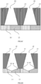
- FIG. 3 is a schematic diagram showing a process of fabricating the SNC structure in existing technologies.
- the isolation structures between the SNC structures include bit line structures and dielectric layer sidewalls, and thus it is required to form the dielectric layer sidewalls when fabricating a groove for containing the SNC structures.
- the dielectric layer sidewalls are difficult to be formed by etching. Therefore, in the related technologies, generally a trench is fabricated (as shown in Step (a)) by etching a sacrificial layer material 31 (which is generally an oxide, such as silicon dioxide, BPSG, BSG, and so on) in the along a B-B line as shown in FIG. 2 , and dielectric layer structures 15 are fabricated (as shown in Step (b)) by using a deposition technology.
- a sacrificial layer material 31 which is generally an oxide, such as silicon dioxide, BPSG, BSG, and so on
- Step (d) the remaining sacrificial layer material 31 is removed (as shown in Step (c)), and a polycrystalline silicon is deposited between the dielectric layer structures 15 to fabricate the SNC structure 11 (as shown in Step (d)).
- isolation structures such as the isolation structures 12 on the right part of the FIG. 1
- the isolation structures including the bit line structures generally are formed before the dielectric layer structures 15 are formed.
- the sacrificial layer material is etched in Step (a), the cross-section of the remaining sacrificial layer material is trapezoid.
- the SNC structure finally fabricated is also a trapezoidal cross section which is narrow at the top and wide at the bottom, making it difficult to complete good deposition of the polycrystalline silicon. Air gaps generally exist in the SNC structure (as shown in Step (d)).
- the embodiments of the present disclosure provide semiconductor structures capable of avoiding a forming of air gaps in the SNC structure.
- FIG. 4 illustrates a schematic diagram of a semiconductor structure according to an embodiment of the present disclosure.
- FIG. 4 is a cross-sectional view along a B-B line of the structure as shown on the left half part of the FIG. 2 , and there exists isolation structures (such as the isolation structures 12 on the right half part of the FIG. 1 ) including the bit line structures in the front and rear of the viewing direction in the figures.
- the semiconductor structure 400 may include:
- FIG. 4 is a cross-sectional view along a B-B line in FIG. 2 , the isolation structures 15 marked in FIG. 4 actually are dielectric layer structures, i.e., the isolation structures 15 on the right half part of FIG. 2 .
- the isolation structures 15 in the embodiments of the present disclosure further include the bit line structures 12 as shown in FIG. 1 , and the bit line structures 12 are in the front or rear of the viewing direction in FIG. 4 . That is, the isolation structures 15 in the embodiments of the present disclosure include four sidewall structures such as two adjacent bit line structures and two adjacent dielectric layer structures, to realize encirclement and isolation of the groove 42.
- a top area of the groove 42 is smaller than a bottom area thereof, and cross-sectional shapes of the plurality of grooves include one or more of a square, a polygon, a circle, or an ellipse.
- the plurality of grooves 42 are arranged in an array, wherein the array may be an aligned or staggered dot array. It is to be understood that two opposite sidewalls of the groove 42 are formed by the isolation structures including the bit line structures, and the bit line structure is perpendicular to the substrate. Therefore, a length of a top surface of the groove 42 may be equal to that of a bottom surface thereof, or a width of the top surface of the groove 42 may be equal to that of the bottom surface, which is not particularly limited in the present disclosure.
- an inclination angle of the first inclined plane 43 may be 30°-40°, for example.
- a slope of the other region is different from that of the first inclined plane, which may be, for example, a horizontal region (for example, a bottom shape of the SNC structure 11 in the structure on the right half part of FIG. 1 ).
- the first inclined plane 43 may also be a cambered surface formed in an etching process, which is not particularly limited in the present disclosure.
- FIG. 5 illustrates a flowchart of a method of fabricating the semiconductor structure as shown in FIG. 4 .
- the method 500 of fabricating the semiconductor structure may include:
- the sacrificial layer is, for example, an oxide layer, including but not limited to materials such as oxide (such as silicon dioxide), BPSG, BSG, and the like.
- the first groove is, for example, an inverted trapezoidal groove which is wide at the top and narrow at the bottom
- the second groove is, for example, a trapezoidal groove which is wide at the bottom and narrow at the top.
- a non-inverted trapezoidal first groove may also be formed here, wherein a shape of the first groove is determined by factors such as technology means and technological conditions; and the second groove may also be a non-trapezoidal groove, wherein a shape of the second groove is related to the shape of the first groove.
- FIG. 6A to FIG. 6D illustrate schematic diagrams of the process of the steps as shown in FIG. 5 .
- FIG. 6A to FIG. 6D are merely for the purpose of illustration, and are not intended to limit the positions and proportions of the active regions and the shallow trench isolation regions in the actual processes.
- the first groove 45 is also etched on the sacrificial layer 44 to make preparations for the subsequent fabrication of the isolation structure.
- the active region 14 and the shallow trench isolation region 13 are exposed at the bottom of the first groove 45 at the same time.
- the bit line structures in the front or rear of the viewing direction of the figures generally have already been formed. Therefore, the step as shown in FIG. 6A actually refers to filling the sacrificial layer between the bit line structures and then etching the first groove 45 in the sacrificial layer. That is, two sidewalls in the front and rear of the viewing direction of the first groove 45 are perpendicular to each other and are formed by the isolation structures including the bit line structures.
- the isolation structures 15 are fabricated in the same way by depositing a dielectric layer, wherein a material of the dielectric layer is, for example, silicon nitride.
- Step (c) in FIG. 3 space is created for the fabrication of the SNC also by removing the sacrificial layer 44 to form the second groove 42, and the active region 14 and the shallow trench isolation region 13 are exposed at the bottom of the second groove 42 at the same time.
- the cross-sectional positions are different (that is, the B-B line is shifted transversely)
- the proportions of the active region and the shallow trench isolation region exposed at the bottom of the second groove 42 actually are different. Therefore, although the embodiments of the present disclosure merely show one type of exposed state of the active region and the shallow trench isolation region, in practical applications, the active region and the shallow trench isolation region may have many types of exposed states.
- the SNC is fabricated by means of an epitaxial silicon growth process. Therefore, for the smooth progress of the epitaxial silicon growth process, the bottom of the second groove 42 is processed. That is, the first inclined plane 43 is fabricated at the bottom of the second groove 42 through a dry etching process or wet etching process, etc.
- both the active region and the shallow trench isolation region are exposed at the bottom of the second groove 42 (referring to the structure on the left half part of FIG. 2 ).
- the material of the active region generally is monocrystalline silicon
- the material of the shallow trench isolation region generally is oxide (for example, silicon dioxide).
- the active region and the shallow trench isolation region provide completely different environments for the growth of the epitaxial silicon.
- the monocrystalline silicon in this process, generally grows only on one side of the monocrystalline silicon, and the monocrystalline silicon is hard to grow or grows at a slow rate on one side of the silicon dioxide. Therefore, to provide more crystal orientations for the growth of the monocrystalline silicon and to ensure the growth of the monocrystalline silicon more uniform and more rapid, the first inclined plane 43 is fabricated before the epitaxial silicon growth process.
- gas for etching the first inclined plane 43 may be, for example, sulfur hexafluoride (SF6).
- the first inclined plane 43 whose inclination angle is 30°-40° may be etched by controlling parameters such as bias and flow of the etching gas. It is to be noted that in the etching process, generally it is unable to ensure that a perfect plane is etched. Therefore, in the actual fabrication processes, the first inclined plane 43 may also be a cambered surface formed by the etching process, wherein the shape of the cambered surface may be as shown in FIG. 7A .
- the active region also likely has other regions such as planes. That is, an end point of the first inclined plane 43 formed by etching does not coincide with an edge of the active region. In this case, the state of the active region may be as shown in FIG. 7B .
- an etching selectivity may be controlled to be, for example, 1:1 to form the second inclined plane 46.
- the inclination angle of the second inclined plane 46 is, for example, 20°-60°.
- the second inclined plane 46 may also be a cambered surface, or the edge of the second inclined plane 46 does not coincide with the edge of the shallow trench isolation region. Reference may be made to FIG. 7A and FIG. 7B respectively for these two states.
- the inclined plane at the bottom of the second groove 42 is actually similar to a bowl shape placed upright. There exists an inclined plane at the bottom of the second groove 42 no matter it is viewed from the cross section along the A-A line in FIG. 1 or it is viewed from the cross section along the B-B line in FIG. 2 .
- FIG. 8A and FIG. 8B viewed from the cross section along the A-A line on the left half part of FIG. 1 , the active region 14 and the shallow trench isolation region 13 may have different proportions and different inclined planes.
- the first inclined plane 43 also may be cleaned in situ by means of dry cleaning of oxides or dry cleaning of removing carbon-based residues, etc., thus the purity of the monocrystalline silicon interface is ensured, so as to obtain high-quality growth effects.
- the monocrystalline silicon may grow, by taking the inclined plane as the substrate, until the epitaxial silicon is controlled to fill the entire second groove 42 up to form the conductive plug 11 as shown in FIG. 4 .
- the conductive plug 11 is a storage node contact (SNC) structure.
- SNC storage node contact
- a growth selectivity of the polycrystalline silicon may be reduced in step S4, and a growth rate of that may be increased.
- the growth selectivity may be reduced by setting an appropriate flow of hydrochloric acid.
- the concentration of the hydrochloric acid is, for example, 150 sccm ⁇ 30%.
- Increase of the flow of the hydrochloric acid may inhibit the growth of polycrystals and tend to grow on the surface of a monocrystal.
- Decrease of the flow of the hydrochloric acid may increase the growth rate of the polycrystalline silicon and increase the yield. Therefore, it is required to seek the most appropriate flow range of the hydrochloric acid to ensure the quality of the monocrystal and to increase the yield. Therefore, the above range is set in the embodiments of the present disclosure.
- the monocrystalline silicon and the polycrystalline silicon may grow at the same time, and thus their shapes are not easy to control, as shown in FIG. 9A or FIG. 9B .
- the polycrystalline silicon may be removed by means of recess etch such as a wet process to only leave the monocrystal silicon, and the shape of the top of the monocrystalline silicon may be trimmed to a plane roughly (as shown in FIG. 10 ), and the length of the conductive plug is adjusted for the subsequent metal connection process.
- the conductive plug is a storage node contact.
- a capacitive landing pad made of a metal material may be formed on the storage node contact for subsequent fabrication of a capacitor on the interface platform.
- the connection of the landing pad made of the metal material onto the storage node contact belongs to the fabrication of a metal-semiconductor contact structure. Therefore, in another embodiment of the present disclosure, after filling the second groove, metal may be deposited on the surface of the conductive plug 11.
- the above-mentioned landing pad is in contact with the monocrystalline silicon, which is a case where metal is in contact with the monocrystalline silicon, similar to the case of contact between a source and a drain of a transistor in a peripheral circuit.
- a metallization process is implemented, and optimal process conditions may be achieved at the same time, which makes process condition requirements simpler, improves the performance of the contact structure, and allows a contact resistance between the metal and the monocrystalline silicon to be smaller under the condition of lower fabrication costs.
- the monocrystalline silicon is grown at the bottom of the groove to fabricate a storage node contact structure (SNC structure) that fills the groove up, which can avoid degradation of electrical properties caused by air gaps formed in the SNC structure due to deposition of the polycrystalline silicon in the related technologies.
- SNC structure storage node contact structure
- problems such as uneven growth and low growth rate caused in the growth process of the monocrystalline silicon may be avoided, and a fabrication efficiency can be effectively enhanced while improving the yield rate.
- an inclined plane is provided on the exposed part of the active region at the bottom of the groove containing the SNC structure, and the polycrystalline silicon is grown inside the groove by taking the inclined plane as a substrate.
- the SNC structure without air gap can be quickly formed, a component failure rate can be reduced, and a yield rate can be enhanced.
Landscapes
- Engineering & Computer Science (AREA)
- Manufacturing & Machinery (AREA)
- Semiconductor Memories (AREA)
- Element Separation (AREA)
Claims (15)
- Structure semi-conductrice, comprenant un substrat (41) et une pluralité de structures d'isolation (15) ; le substrat (41) comprend des régions actives (14) et des régions d'isolation par tranchées peu profondes (13) disposées à des intervalles les unes des autres ; la pluralité de structures d'isolation (15) sont disposées sur une surface du substrat (41) ;une pluralité de rainures (42), disposées entre la pluralité de structures d'isolation (15), un fond de chacune des rainures (42) étant pourvu d'un premier biseau (43), et le premier biseau (43) étant formé dans chacune des régions actives (14) ; etune fiche conductrice (11), disposée dans chacune des rainures (42) ; caractérisée en ce quela fiche conductrice (11) est produit par croissance épitaxiale sur le premier biseau (43) et formée dans chacune des rainures (42), et une zone supérieure de la fiche conductrice (11) est plus petite qu'une zone inférieure de la fiche conductrice (11).
- Structure semi-conductrice selon la revendication 1, caractérisée en ce qu'une zone supérieure de chacune des rainures (42) est plus petite qu'une zone inférieure de la rainure (42).
- Structure semi-conductrice selon la revendication 1, caractérisée en ce qu'un angle d'inclinaison du premier biseau (43) est de 30° à 40°.
- Structure semi-conductrice selon la revendication 1, caractérisée en ce qu'un fond de chacune des rainures (42) est en outre pourvu d'un second biseau (46), et en ce que le second biseau (46) est formé sur chacune des régions d'isolation par tranchées peu profondes (13).
- Structure semi-conductrice selon la revendication 4, caractérisée en ce qu'un angle d'inclinaison du second biseau (46) est de 20° à 60°.
- Structure semi-conductrice selon la revendication 1, caractérisée en ce que la pluralité de structures d'isolation (15) comprend des structures de couches diélectriques.
- Structure semi-conductrice selon la revendication 1, caractérisée en ce que les formes des sections transversales de la pluralité de rainures (42) comprennent un ou plusieurs d'un polygone, un cercle ou une ellipse.
- Structure semi-conductrice selon la revendication 7, caractérisée en ce que la pluralité de rainures (42) est disposée en réseau.
- Structure semi-conductrice selon la revendication 1, caractérisée en ce que le premier biseau (43) est une surface bombée.
- Procédé de fabrication d'une structure semi-conductrice, comprenant :la fourniture d'un substrat (41), le substrat (41) comprenant des régions actives (14) et des régions d'isolation par tranchées peu profondes (13) disposées à des intervalles les unes des autres ;la formation d'un matériau de couche sacrificielle (31) sur une surface du substrat (41) ;la gravure d'une partie du matériau de couche sacrificielle (31) pour former une pluralité de premières rainures (45) ; le retrait du matériau de couche sacrificielle (31) restant pour former une pluralité de secondes rainures (42) après avoir déposé une couche diélectrique sur la pluralité de premières rainures (45) ;la gravure d'une partie exposée de chacune des régions actives (14) au fond de chacune des secondes rainures (42) pour former un premier biseau (43) ; etla réalisation d'un processus de croissance épitaxiale sur le premier biseau (43) pour former une fiche conductrice (11) dans chacune des secondes rainures (42), dans lequel une zone supérieure de la fiche conductrice (11) est plus petite qu'une zone inférieure de la fiche conductrice (11).
- Procédé selon la revendication 10, caractérisé en ce que l'angle d'inclinaison du premier biseau (43) est de 30° à 40°.
- Procédé selon la revendication 10, caractérisé en ce que l'étape de gravure d'une partie exposée de chacune des régions actives (14) au fond de chacune des secondes rainures (42) pour former un premier biseau (43) comprend en outre :
la gravure simultanée d'une partie exposée de chacune des régions d'isolation par tranchées peu profondes (13) adjacente à la partie exposée de chacune des régions actives (14) pour former un second biseau (46). - Procédé selon la revendication 12, caractérisé en ce qu'une sélectivité de gravure de la partie exposée de chacune des régions actives (14) par rapport à une sélectivité de gravure de la partie exposée de chacune des régions d'isolation par tranchées peu profondes (13) est de 1:1.
- Procédé selon la revendication 10, caractérisé en ce qu'il comprend en outre : le dépôt de métal sur une surface de la fiche conductrice (11).
- Procédé selon la revendication 14, caractérisé en ce qu'il comprend en outre :
avant le dépôt du métal, le retrait, de la fiche conductrice (11), d'un silicium polycristallin en utilisant un procédé humide pour ne conserver qu'un silicium monocristallin, et la découpe de la partie supérieure du silicium rempli pour en faire un plan plat.
Applications Claiming Priority (2)
| Application Number | Priority Date | Filing Date | Title |
|---|---|---|---|
| CN201911239722.1A CN112928094B (zh) | 2019-12-06 | 2019-12-06 | 半导体结构及其制造方法 |
| PCT/CN2020/102476 WO2021109580A1 (fr) | 2019-12-06 | 2020-07-16 | Structure semi-conductrice et son procédé de fabrication |
Publications (3)
| Publication Number | Publication Date |
|---|---|
| EP3968371A1 EP3968371A1 (fr) | 2022-03-16 |
| EP3968371A4 EP3968371A4 (fr) | 2022-08-31 |
| EP3968371B1 true EP3968371B1 (fr) | 2023-06-28 |
Family
ID=76161402
Family Applications (1)
| Application Number | Title | Priority Date | Filing Date |
|---|---|---|---|
| EP20896064.1A Active EP3968371B1 (fr) | 2019-12-06 | 2020-07-16 | Structure semi-conductrice et son procédé de fabrication |
Country Status (4)
| Country | Link |
|---|---|
| US (1) | US20210320107A1 (fr) |
| EP (1) | EP3968371B1 (fr) |
| CN (1) | CN112928094B (fr) |
| WO (1) | WO2021109580A1 (fr) |
Families Citing this family (4)
| Publication number | Priority date | Publication date | Assignee | Title |
|---|---|---|---|---|
| CN115116962B (zh) * | 2021-03-22 | 2024-06-07 | 长鑫存储技术有限公司 | 半导体结构的制备方法和半导体结构 |
| CN116130409B (zh) * | 2021-11-15 | 2026-02-17 | 长鑫存储技术有限公司 | 接触结构的形成方法、半导体结构及存储器 |
| CN115274547A (zh) * | 2022-08-26 | 2022-11-01 | 长鑫存储技术有限公司 | 半导体结构的制备方法、半导体结构及隔离结构 |
| CN117529097B (zh) * | 2023-12-28 | 2024-04-19 | 长鑫集电(北京)存储技术有限公司 | 半导体结构及其制备方法 |
Family Cites Families (11)
| Publication number | Priority date | Publication date | Assignee | Title |
|---|---|---|---|---|
| KR20090072092A (ko) * | 2007-12-28 | 2009-07-02 | 주식회사 하이닉스반도체 | 반도체 소자 및 이의 제조 방법 |
| KR101660782B1 (ko) * | 2010-07-29 | 2016-09-29 | 삼성전자주식회사 | 메모리 소자 및 이의 제조방법 |
| KR101805182B1 (ko) * | 2012-01-31 | 2017-12-06 | 에스케이하이닉스 주식회사 | 전도성 플러그를 구비하는 반도체 소자 및 그 제조 방법 |
| KR102057073B1 (ko) * | 2013-07-26 | 2019-12-18 | 에스케이하이닉스 주식회사 | 트렌치 내부에 배치되는 비트라인 구조물을 구비하는 반도체 소자, 이를 포함하는 패키지, 모듈 및 시스템 |
| US9425200B2 (en) * | 2013-11-07 | 2016-08-23 | SK Hynix Inc. | Semiconductor device including air gaps and method for fabricating the same |
| KR102509322B1 (ko) * | 2017-09-29 | 2023-03-14 | 에스케이하이닉스 주식회사 | 에어갭을 구비한 반도체장치 및 그 제조 방법 |
| KR102396583B1 (ko) * | 2017-11-09 | 2022-05-11 | 삼성전자주식회사 | 메모리 소자 및 이의 제조방법 |
| CN208655651U (zh) * | 2018-09-19 | 2019-03-26 | 长鑫存储技术有限公司 | 埋入式字线结构及存储器 |
| CN208767278U (zh) * | 2018-10-11 | 2019-04-19 | 长鑫存储技术有限公司 | 半导体器件 |
| KR102476141B1 (ko) * | 2018-12-14 | 2022-12-09 | 삼성전자주식회사 | 스페이서를 포함하는 반도체 소자 및 그 제조 방법 |
| CN210926003U (zh) * | 2019-12-06 | 2020-07-03 | 长鑫存储技术有限公司 | 半导体结构 |
-
2019
- 2019-12-06 CN CN201911239722.1A patent/CN112928094B/zh active Active
-
2020
- 2020-07-16 WO PCT/CN2020/102476 patent/WO2021109580A1/fr not_active Ceased
- 2020-07-16 EP EP20896064.1A patent/EP3968371B1/fr active Active
-
2021
- 2021-06-24 US US17/356,521 patent/US20210320107A1/en not_active Abandoned
Also Published As
| Publication number | Publication date |
|---|---|
| CN112928094A (zh) | 2021-06-08 |
| CN112928094B (zh) | 2025-01-10 |
| US20210320107A1 (en) | 2021-10-14 |
| EP3968371A4 (fr) | 2022-08-31 |
| EP3968371A1 (fr) | 2022-03-16 |
| WO2021109580A1 (fr) | 2021-06-10 |
Similar Documents
| Publication | Publication Date | Title |
|---|---|---|
| EP3968371B1 (fr) | Structure semi-conductrice et son procédé de fabrication | |
| US11056507B2 (en) | Memory arrays and methods used in forming a memory array | |
| EP3210242B1 (fr) | Chaînes de mémoire non-et et leurs procédés de fabrication | |
| US20210313347A1 (en) | Stacked structure for a vertical memory device | |
| US11462544B2 (en) | Array of recessed access gate lines | |
| US11895838B2 (en) | Vertical memory devices | |
| CN110890365A (zh) | 一种半导体存储器及其制备方法 | |
| US12340870B2 (en) | Method for forming a semiconductor device pillar with source, channel, and drain | |
| WO2023216396A1 (fr) | Structure semi-conductrice et son procédé de formation | |
| CN210926003U (zh) | 半导体结构 | |
| US20250343167A1 (en) | Vertical memory devices including insulating interlayer covering circuit pattern and intermediate insulation layer on the insulating interlayer | |
| US8124481B2 (en) | Semiconductor device for reducing interference between adjoining gates and method for manufacturing the same | |
| WO2022062644A1 (fr) | Structure semi-conductrice et son procédé de préparation, et dispositif de stockage | |
| US20200357809A1 (en) | Memory Arrays And Methods Used In Forming A Memory Array | |
| KR20010010442A (ko) | 반도체 소자의 콘택 패드 형성 방법 | |
| CN118102709A (zh) | 半导体结构及其形成方法 | |
| WO2023206812A1 (fr) | Structure semi-conductrice et son procédé de fabrication, et mémoire | |
| US6291293B1 (en) | Method for fabricating an open can-type stacked capacitor on an uneven surface | |
| CN118900557B (zh) | 半导体结构及其制作方法 | |
| KR101458959B1 (ko) | 셰어드 비트라인 구조를 갖는 반도체 장치 및 그 제조방법 | |
| CN119012683B (zh) | 半导体结构的制造方法及半导体结构 | |
| US7867865B2 (en) | Methods of fabricating semiconductor devices including elevated source and drain regions | |
| US20240215228A1 (en) | Semiconductor integrated circuit device including a word line with variable widths | |
| WO2024050951A1 (fr) | Structure semi-conductrice et son procédé de formation | |
| CN119277775A (zh) | 半导体装置 |
Legal Events
| Date | Code | Title | Description |
|---|---|---|---|
| STAA | Information on the status of an ep patent application or granted ep patent |
Free format text: STATUS: THE INTERNATIONAL PUBLICATION HAS BEEN MADE |
|
| PUAI | Public reference made under article 153(3) epc to a published international application that has entered the european phase |
Free format text: ORIGINAL CODE: 0009012 |
|
| STAA | Information on the status of an ep patent application or granted ep patent |
Free format text: STATUS: REQUEST FOR EXAMINATION WAS MADE |
|
| 17P | Request for examination filed |
Effective date: 20211210 |
|
| AK | Designated contracting states |
Kind code of ref document: A1 Designated state(s): AL AT BE BG CH CY CZ DE DK EE ES FI FR GB GR HR HU IE IS IT LI LT LU LV MC MK MT NL NO PL PT RO RS SE SI SK SM TR |
|
| REG | Reference to a national code |
Ref country code: DE Ref legal event code: R079 Free format text: PREVIOUS MAIN CLASS: H01L0023528000 Ipc: H01L0021768000 Ref document number: 602020013149 Country of ref document: DE |
|
| A4 | Supplementary search report drawn up and despatched |
Effective date: 20220728 |
|
| RIC1 | Information provided on ipc code assigned before grant |
Ipc: H01L 21/285 20060101ALI20220722BHEP Ipc: H01L 27/108 20060101ALI20220722BHEP Ipc: H01L 21/768 20060101AFI20220722BHEP |
|
| DAV | Request for validation of the european patent (deleted) | ||
| DAX | Request for extension of the european patent (deleted) | ||
| GRAJ | Information related to disapproval of communication of intention to grant by the applicant or resumption of examination proceedings by the epo deleted |
Free format text: ORIGINAL CODE: EPIDOSDIGR1 |
|
| STAA | Information on the status of an ep patent application or granted ep patent |
Free format text: STATUS: GRANT OF PATENT IS INTENDED |
|
| GRAP | Despatch of communication of intention to grant a patent |
Free format text: ORIGINAL CODE: EPIDOSNIGR1 |
|
| RIC1 | Information provided on ipc code assigned before grant |
Ipc: H10B 12/00 20230101ALI20230328BHEP Ipc: H01L 21/285 20060101ALI20230328BHEP Ipc: H01L 21/768 20060101AFI20230328BHEP |
|
| INTG | Intention to grant announced |
Effective date: 20230418 |
|
| GRAS | Grant fee paid |
Free format text: ORIGINAL CODE: EPIDOSNIGR3 |
|
| GRAA | (expected) grant |
Free format text: ORIGINAL CODE: 0009210 |
|
| STAA | Information on the status of an ep patent application or granted ep patent |
Free format text: STATUS: THE PATENT HAS BEEN GRANTED |
|
| AK | Designated contracting states |
Kind code of ref document: B1 Designated state(s): AL AT BE BG CH CY CZ DE DK EE ES FI FR GB GR HR HU IE IS IT LI LT LU LV MC MK MT NL NO PL PT RO RS SE SI SK SM TR |
|
| REG | Reference to a national code |
Ref country code: CH Ref legal event code: EP |
|
| P01 | Opt-out of the competence of the unified patent court (upc) registered |
Effective date: 20230531 |
|
| REG | Reference to a national code |
Ref country code: AT Ref legal event code: REF Ref document number: 1583500 Country of ref document: AT Kind code of ref document: T Effective date: 20230715 |
|
| REG | Reference to a national code |
Ref country code: IE Ref legal event code: FG4D |
|
| REG | Reference to a national code |
Ref country code: DE Ref legal event code: R096 Ref document number: 602020013149 Country of ref document: DE |
|
| REG | Reference to a national code |
Ref country code: LT Ref legal event code: MG9D |
|
| PG25 | Lapsed in a contracting state [announced via postgrant information from national office to epo] |
Ref country code: SE Free format text: LAPSE BECAUSE OF FAILURE TO SUBMIT A TRANSLATION OF THE DESCRIPTION OR TO PAY THE FEE WITHIN THE PRESCRIBED TIME-LIMIT Effective date: 20230628 Ref country code: NO Free format text: LAPSE BECAUSE OF FAILURE TO SUBMIT A TRANSLATION OF THE DESCRIPTION OR TO PAY THE FEE WITHIN THE PRESCRIBED TIME-LIMIT Effective date: 20230928 |
|
| REG | Reference to a national code |
Ref country code: NL Ref legal event code: MP Effective date: 20230628 |
|
| REG | Reference to a national code |
Ref country code: AT Ref legal event code: MK05 Ref document number: 1583500 Country of ref document: AT Kind code of ref document: T Effective date: 20230628 |
|
| PG25 | Lapsed in a contracting state [announced via postgrant information from national office to epo] |
Ref country code: RS Free format text: LAPSE BECAUSE OF FAILURE TO SUBMIT A TRANSLATION OF THE DESCRIPTION OR TO PAY THE FEE WITHIN THE PRESCRIBED TIME-LIMIT Effective date: 20230628 Ref country code: NL Free format text: LAPSE BECAUSE OF FAILURE TO SUBMIT A TRANSLATION OF THE DESCRIPTION OR TO PAY THE FEE WITHIN THE PRESCRIBED TIME-LIMIT Effective date: 20230628 Ref country code: LV Free format text: LAPSE BECAUSE OF FAILURE TO SUBMIT A TRANSLATION OF THE DESCRIPTION OR TO PAY THE FEE WITHIN THE PRESCRIBED TIME-LIMIT Effective date: 20230628 Ref country code: LT Free format text: LAPSE BECAUSE OF FAILURE TO SUBMIT A TRANSLATION OF THE DESCRIPTION OR TO PAY THE FEE WITHIN THE PRESCRIBED TIME-LIMIT Effective date: 20230628 Ref country code: HR Free format text: LAPSE BECAUSE OF FAILURE TO SUBMIT A TRANSLATION OF THE DESCRIPTION OR TO PAY THE FEE WITHIN THE PRESCRIBED TIME-LIMIT Effective date: 20230628 Ref country code: GR Free format text: LAPSE BECAUSE OF FAILURE TO SUBMIT A TRANSLATION OF THE DESCRIPTION OR TO PAY THE FEE WITHIN THE PRESCRIBED TIME-LIMIT Effective date: 20230929 |
|
| PG25 | Lapsed in a contracting state [announced via postgrant information from national office to epo] |
Ref country code: FI Free format text: LAPSE BECAUSE OF FAILURE TO SUBMIT A TRANSLATION OF THE DESCRIPTION OR TO PAY THE FEE WITHIN THE PRESCRIBED TIME-LIMIT Effective date: 20230628 |
|
| PG25 | Lapsed in a contracting state [announced via postgrant information from national office to epo] |
Ref country code: SK Free format text: LAPSE BECAUSE OF FAILURE TO SUBMIT A TRANSLATION OF THE DESCRIPTION OR TO PAY THE FEE WITHIN THE PRESCRIBED TIME-LIMIT Effective date: 20230628 |
|
| PG25 | Lapsed in a contracting state [announced via postgrant information from national office to epo] |
Ref country code: ES Free format text: LAPSE BECAUSE OF FAILURE TO SUBMIT A TRANSLATION OF THE DESCRIPTION OR TO PAY THE FEE WITHIN THE PRESCRIBED TIME-LIMIT Effective date: 20230628 |
|
| PG25 | Lapsed in a contracting state [announced via postgrant information from national office to epo] |
Ref country code: IS Free format text: LAPSE BECAUSE OF FAILURE TO SUBMIT A TRANSLATION OF THE DESCRIPTION OR TO PAY THE FEE WITHIN THE PRESCRIBED TIME-LIMIT Effective date: 20231028 |
|
| PG25 | Lapsed in a contracting state [announced via postgrant information from national office to epo] |
Ref country code: SM Free format text: LAPSE BECAUSE OF FAILURE TO SUBMIT A TRANSLATION OF THE DESCRIPTION OR TO PAY THE FEE WITHIN THE PRESCRIBED TIME-LIMIT Effective date: 20230628 Ref country code: SK Free format text: LAPSE BECAUSE OF FAILURE TO SUBMIT A TRANSLATION OF THE DESCRIPTION OR TO PAY THE FEE WITHIN THE PRESCRIBED TIME-LIMIT Effective date: 20230628 Ref country code: RO Free format text: LAPSE BECAUSE OF FAILURE TO SUBMIT A TRANSLATION OF THE DESCRIPTION OR TO PAY THE FEE WITHIN THE PRESCRIBED TIME-LIMIT Effective date: 20230628 Ref country code: PT Free format text: LAPSE BECAUSE OF FAILURE TO SUBMIT A TRANSLATION OF THE DESCRIPTION OR TO PAY THE FEE WITHIN THE PRESCRIBED TIME-LIMIT Effective date: 20231030 Ref country code: IS Free format text: LAPSE BECAUSE OF FAILURE TO SUBMIT A TRANSLATION OF THE DESCRIPTION OR TO PAY THE FEE WITHIN THE PRESCRIBED TIME-LIMIT Effective date: 20231028 Ref country code: ES Free format text: LAPSE BECAUSE OF FAILURE TO SUBMIT A TRANSLATION OF THE DESCRIPTION OR TO PAY THE FEE WITHIN THE PRESCRIBED TIME-LIMIT Effective date: 20230628 Ref country code: EE Free format text: LAPSE BECAUSE OF FAILURE TO SUBMIT A TRANSLATION OF THE DESCRIPTION OR TO PAY THE FEE WITHIN THE PRESCRIBED TIME-LIMIT Effective date: 20230628 Ref country code: CZ Free format text: LAPSE BECAUSE OF FAILURE TO SUBMIT A TRANSLATION OF THE DESCRIPTION OR TO PAY THE FEE WITHIN THE PRESCRIBED TIME-LIMIT Effective date: 20230628 Ref country code: AT Free format text: LAPSE BECAUSE OF FAILURE TO SUBMIT A TRANSLATION OF THE DESCRIPTION OR TO PAY THE FEE WITHIN THE PRESCRIBED TIME-LIMIT Effective date: 20230628 |
|
| PG25 | Lapsed in a contracting state [announced via postgrant information from national office to epo] |
Ref country code: PL Free format text: LAPSE BECAUSE OF FAILURE TO SUBMIT A TRANSLATION OF THE DESCRIPTION OR TO PAY THE FEE WITHIN THE PRESCRIBED TIME-LIMIT Effective date: 20230628 |
|
| REG | Reference to a national code |
Ref country code: CH Ref legal event code: PL |
|
| PG25 | Lapsed in a contracting state [announced via postgrant information from national office to epo] |
Ref country code: MC Free format text: LAPSE BECAUSE OF FAILURE TO SUBMIT A TRANSLATION OF THE DESCRIPTION OR TO PAY THE FEE WITHIN THE PRESCRIBED TIME-LIMIT Effective date: 20230628 |
|
| REG | Reference to a national code |
Ref country code: BE Ref legal event code: MM Effective date: 20230731 |
|
| PG25 | Lapsed in a contracting state [announced via postgrant information from national office to epo] |
Ref country code: LU Free format text: LAPSE BECAUSE OF NON-PAYMENT OF DUE FEES Effective date: 20230716 |
|
| PG25 | Lapsed in a contracting state [announced via postgrant information from national office to epo] |
Ref country code: MC Free format text: LAPSE BECAUSE OF FAILURE TO SUBMIT A TRANSLATION OF THE DESCRIPTION OR TO PAY THE FEE WITHIN THE PRESCRIBED TIME-LIMIT Effective date: 20230628 Ref country code: LU Free format text: LAPSE BECAUSE OF NON-PAYMENT OF DUE FEES Effective date: 20230716 |
|
| REG | Reference to a national code |
Ref country code: DE Ref legal event code: R097 Ref document number: 602020013149 Country of ref document: DE |
|
| REG | Reference to a national code |
Ref country code: IE Ref legal event code: MM4A |
|
| PG25 | Lapsed in a contracting state [announced via postgrant information from national office to epo] |
Ref country code: DK Free format text: LAPSE BECAUSE OF FAILURE TO SUBMIT A TRANSLATION OF THE DESCRIPTION OR TO PAY THE FEE WITHIN THE PRESCRIBED TIME-LIMIT Effective date: 20230628 Ref country code: CH Free format text: LAPSE BECAUSE OF NON-PAYMENT OF DUE FEES Effective date: 20230731 |
|
| PLBE | No opposition filed within time limit |
Free format text: ORIGINAL CODE: 0009261 |
|
| STAA | Information on the status of an ep patent application or granted ep patent |
Free format text: STATUS: NO OPPOSITION FILED WITHIN TIME LIMIT |
|
| PG25 | Lapsed in a contracting state [announced via postgrant information from national office to epo] |
Ref country code: IT Free format text: LAPSE BECAUSE OF FAILURE TO SUBMIT A TRANSLATION OF THE DESCRIPTION OR TO PAY THE FEE WITHIN THE PRESCRIBED TIME-LIMIT Effective date: 20230628 Ref country code: BE Free format text: LAPSE BECAUSE OF NON-PAYMENT OF DUE FEES Effective date: 20230731 |
|
| 26N | No opposition filed |
Effective date: 20240402 |
|
| PG25 | Lapsed in a contracting state [announced via postgrant information from national office to epo] |
Ref country code: IE Free format text: LAPSE BECAUSE OF NON-PAYMENT OF DUE FEES Effective date: 20230716 |
|
| PG25 | Lapsed in a contracting state [announced via postgrant information from national office to epo] |
Ref country code: IE Free format text: LAPSE BECAUSE OF NON-PAYMENT OF DUE FEES Effective date: 20230716 Ref country code: SI Free format text: LAPSE BECAUSE OF FAILURE TO SUBMIT A TRANSLATION OF THE DESCRIPTION OR TO PAY THE FEE WITHIN THE PRESCRIBED TIME-LIMIT Effective date: 20230628 |
|
| PG25 | Lapsed in a contracting state [announced via postgrant information from national office to epo] |
Ref country code: BG Free format text: LAPSE BECAUSE OF FAILURE TO SUBMIT A TRANSLATION OF THE DESCRIPTION OR TO PAY THE FEE WITHIN THE PRESCRIBED TIME-LIMIT Effective date: 20230628 |
|
| PG25 | Lapsed in a contracting state [announced via postgrant information from national office to epo] |
Ref country code: BG Free format text: LAPSE BECAUSE OF FAILURE TO SUBMIT A TRANSLATION OF THE DESCRIPTION OR TO PAY THE FEE WITHIN THE PRESCRIBED TIME-LIMIT Effective date: 20230628 |
|
| PG25 | Lapsed in a contracting state [announced via postgrant information from national office to epo] |
Ref country code: CY Free format text: LAPSE BECAUSE OF FAILURE TO SUBMIT A TRANSLATION OF THE DESCRIPTION OR TO PAY THE FEE WITHIN THE PRESCRIBED TIME-LIMIT; INVALID AB INITIO Effective date: 20200716 |
|
| PG25 | Lapsed in a contracting state [announced via postgrant information from national office to epo] |
Ref country code: HU Free format text: LAPSE BECAUSE OF FAILURE TO SUBMIT A TRANSLATION OF THE DESCRIPTION OR TO PAY THE FEE WITHIN THE PRESCRIBED TIME-LIMIT; INVALID AB INITIO Effective date: 20200716 |
|
| PGFP | Annual fee paid to national office [announced via postgrant information from national office to epo] |
Ref country code: DE Payment date: 20250722 Year of fee payment: 6 |
|
| PGFP | Annual fee paid to national office [announced via postgrant information from national office to epo] |
Ref country code: GB Payment date: 20250722 Year of fee payment: 6 |
|
| PGFP | Annual fee paid to national office [announced via postgrant information from national office to epo] |
Ref country code: FR Payment date: 20250725 Year of fee payment: 6 |
|
| REG | Reference to a national code |
Ref country code: DE Ref legal event code: R079 Ref document number: 602020013149 Country of ref document: DE Free format text: PREVIOUS MAIN CLASS: H01L0021768000 Ipc: H10W0020000000 |
|
| PG25 | Lapsed in a contracting state [announced via postgrant information from national office to epo] |
Ref country code: TR Free format text: LAPSE BECAUSE OF FAILURE TO SUBMIT A TRANSLATION OF THE DESCRIPTION OR TO PAY THE FEE WITHIN THE PRESCRIBED TIME-LIMIT Effective date: 20230628 |