EP3970176B1 - Elektronisches installationsgerät - Google Patents
Elektronisches installationsgerät Download PDFInfo
- Publication number
- EP3970176B1 EP3970176B1 EP20732882.4A EP20732882A EP3970176B1 EP 3970176 B1 EP3970176 B1 EP 3970176B1 EP 20732882 A EP20732882 A EP 20732882A EP 3970176 B1 EP3970176 B1 EP 3970176B1
- Authority
- EP
- European Patent Office
- Prior art keywords
- electronic installation
- circuit
- installation device
- accordance
- load
- Prior art date
- Legal status (The legal status is an assumption and is not a legal conclusion. Google has not performed a legal analysis and makes no representation as to the accuracy of the status listed.)
- Active
Links
Images


Classifications
-
- H—ELECTRICITY
- H02—GENERATION; CONVERSION OR DISTRIBUTION OF ELECTRIC POWER
- H02H—EMERGENCY PROTECTIVE CIRCUIT ARRANGEMENTS
- H02H3/00—Emergency protective circuit arrangements for automatic disconnection directly responsive to an undesired change from normal electric working condition with or without subsequent reconnection ; integrated protection
- H02H3/08—Emergency protective circuit arrangements for automatic disconnection directly responsive to an undesired change from normal electric working condition with or without subsequent reconnection ; integrated protection responsive to excess current
- H02H3/10—Emergency protective circuit arrangements for automatic disconnection directly responsive to an undesired change from normal electric working condition with or without subsequent reconnection ; integrated protection responsive to excess current additionally responsive to some other abnormal electrical conditions
-
- H—ELECTRICITY
- H01—ELECTRIC ELEMENTS
- H01H—ELECTRIC SWITCHES; RELAYS; SELECTORS; EMERGENCY PROTECTIVE DEVICES
- H01H71/00—Details of the protective switches or relays covered by groups H01H73/00 - H01H83/00
- H01H71/10—Operating or release mechanisms
- H01H71/12—Automatic release mechanisms with or without manual release
- H01H71/40—Combined electrothermal and electromagnetic mechanisms
-
- H—ELECTRICITY
- H02—GENERATION; CONVERSION OR DISTRIBUTION OF ELECTRIC POWER
- H02H—EMERGENCY PROTECTIVE CIRCUIT ARRANGEMENTS
- H02H3/00—Emergency protective circuit arrangements for automatic disconnection directly responsive to an undesired change from normal electric working condition with or without subsequent reconnection ; integrated protection
- H02H3/08—Emergency protective circuit arrangements for automatic disconnection directly responsive to an undesired change from normal electric working condition with or without subsequent reconnection ; integrated protection responsive to excess current
- H02H3/085—Emergency protective circuit arrangements for automatic disconnection directly responsive to an undesired change from normal electric working condition with or without subsequent reconnection ; integrated protection responsive to excess current making use of a thermal sensor, e.g. thermistor, heated by the excess current
-
- H—ELECTRICITY
- H01—ELECTRIC ELEMENTS
- H01H—ELECTRIC SWITCHES; RELAYS; SELECTORS; EMERGENCY PROTECTIVE DEVICES
- H01H85/00—Protective devices in which the current flows through a part of fusible material and this current is interrupted by displacement of the fusible material when this current becomes excessive
- H01H85/02—Details
- H01H85/0241—Structural association of a fuse and another component or apparatus
- H01H2085/0283—Structural association with a semiconductor device
-
- H—ELECTRICITY
- H01—ELECTRIC ELEMENTS
- H01H—ELECTRIC SWITCHES; RELAYS; SELECTORS; EMERGENCY PROTECTIVE DEVICES
- H01H47/00—Circuit arrangements not adapted to a particular application of the relay and designed to obtain desired operating characteristics or to provide energising current
- H01H47/22—Circuit arrangements not adapted to a particular application of the relay and designed to obtain desired operating characteristics or to provide energising current for supplying energising current for relay coil
-
- H—ELECTRICITY
- H01—ELECTRIC ELEMENTS
- H01H—ELECTRIC SWITCHES; RELAYS; SELECTORS; EMERGENCY PROTECTIVE DEVICES
- H01H85/00—Protective devices in which the current flows through a part of fusible material and this current is interrupted by displacement of the fusible material when this current becomes excessive
- H01H85/02—Details
- H01H85/04—Fuses, i.e. expendable parts of the protective device, e.g. cartridges
- H01H85/041—Fuses, i.e. expendable parts of the protective device, e.g. cartridges characterised by the type
- H01H85/046—Fuses formed as printed circuits
-
- H—ELECTRICITY
- H01—ELECTRIC ELEMENTS
- H01H—ELECTRIC SWITCHES; RELAYS; SELECTORS; EMERGENCY PROTECTIVE DEVICES
- H01H89/00—Combinations of two or more different basic types of electric switches, relays, selectors and emergency protective devices, not covered by any single one of the other main groups of this subclass
-
- H—ELECTRICITY
- H05—ELECTRIC TECHNIQUES NOT OTHERWISE PROVIDED FOR
- H05K—PRINTED CIRCUITS; CASINGS OR CONSTRUCTIONAL DETAILS OF ELECTRIC APPARATUS; MANUFACTURE OF ASSEMBLAGES OF ELECTRICAL COMPONENTS
- H05K1/00—Printed circuits
- H05K1/02—Details
- H05K1/0296—Conductive pattern lay-out details not covered by sub groups H05K1/02 - H05K1/0295
- H05K1/0298—Multilayer circuits
Definitions
- the invention relates to an electronic installation device according to the preamble of claim 1.
- An installation device according to the preamble of claim 1 is from DE 10 2017 110897 A1 known.
- Electronic installation devices of this type can contain switch contacts, e.g. of a relay, or power semiconductor components for carrying current under load and electronic control devices for driving a relay coil or for driving power semiconductor components.
- Such electronic installation devices are often used in electrical installation systems for building technology and are designed for a load current that is well below the nominal current, e.g. 16 amperes, of the circuits that are usual in building installation.
- a load current that is well below the nominal current, e.g. 16 amperes, of the circuits that are usual in building installation.
- blind switches, timers, etc. are designed for a load current in the range between 3 amperes and 8 amperes.
- the electronic installation devices must be tested with the tripping current of an upstream fuse element, preferably a miniature circuit breaker, of the building installation when tested in accordance with the standards. Due to the difference between the load current of an electronic installation device and the tripping current of the upstream building-side safety element, the electronic installation device would be protected insufficiently, namely too high. In the event of an overcurrent in the range between the device's rated current and the tripping current of the upstream fuse element of the building installation, the electronic installation device would be unprotected and could be destroyed.
- an upstream fuse element preferably a miniature circuit breaker
- overload is defined as exceeding the permissible current in the electrically undamaged circuit.
- the current-related heat development destroys electrical conductors and components by exceeding permissible limit temperatures.
- An overload protection device detects the heating of conductors and/or components and switches off the circuit at least temporarily.
- Short-circuit currents and overload currents result in different technical requirements for protective devices. Both in the event of a short circuit and an overload, current-carrying lines heat up to impermissibly high temperatures. The main difference is that in the event of a short-circuit with high short-circuit currents, the inadmissibly high amount of heat can be reached in fractions of an electrical half-wave. Even with high short-circuit currents, fuses melt within a sufficiently short time. In the event of an overload, currents occur that are only slightly above the maximum permissible load capacity of a cable and only heat up the cable to impermissibly high temperatures after a long period of time. In such a loaded circuit, a preferably reversible fuse can ensure that the impermissible high temperature cannot be reached on the conductors and components and there is protection against overload.
- self-resetting fuses for example electrical components with PTC characteristics (positive temperature coefficient)
- PTC characteristics positive temperature coefficient
- PTC thermistor has low resistance at normal temperature. If the PTC thermistor heats up, for example due to an external heat supply, it becomes highly resistive, which severely restricts the current flow. If the heat supply is reduced, the PTC thermistor cools down and becomes low-resistance again.
- Electronic installation devices are mainly implemented in small parts on conductor track packages.
- An implementation of a complete overcurrent protection based on printed conductor structures is not yet known, since In particular, the usual conductor path geometry with low layer thicknesses and large surfaces is not suitable for loading with different current limit values.
- Short-circuit protection with a fuse requires a higher melting integral at all other points of the conductor track structure and consequently large conductor track surfaces.
- the heat generation and dissipation of a conductor required for overload protection by means of PTC elements cannot be realized with the usual width of the conductor track. However, a required tapered conductor track would be destroyed in the event of a short circuit.
- a realization of an overload protection based on PTC means that no separate short-circuit protection would be possible on the printed conductor package.
- the corresponding fuse in the house installation usually a reversible automatic device, would have to be replaced according to the lower nominal current of the installation device.
- the object of the present invention is therefore to eliminate the disadvantages mentioned above and to implement an electronic installation device with device-specific protection devices against short circuits and against overload.
- the invention according to claim 1 has the advantage that the electronic installation device according to the invention by a combination of two specific coordinated protective devices is protected against overcurrent.
- a first overcurrent protection device protects against a short circuit, while a second overcurrent protection device protects against overload.
- the electronic installation device can be connected in series with a load.
- the electronic installation device includes a load circuit and a control circuit, which are thermally and physically/electrically coupled.
- the load circuit includes a first overcurrent protection device, a resistive element, and a circuit breaking element, which are positionable in series between a power source and an electrical load.
- An overcurrent detection device interacts with a control device as a second overcurrent protection device.
- the control device is arranged in the control circuit and is operatively connected to the circuit-breaking element in the load circuit.
- the overcurrent detection device can comprise a sensor element in the control circuit, preferably a reversible electrical component, for example in the form of a positive temperature coefficient (PTC) thermistor, and a resistance element in the load circuit which is thermally coupled to the PTC element.
- the resistance element runs as a galvanically isolated conductor below the PTC element.
- the electronic installation device can be implemented at least partially on a printed circuit board arrangement and can have the first overcurrent protection device in the form of a fuse in the load circuit, which protects the device's own electrical components and conductors in the event of a short circuit. This means that the melting integral of the protected components and conductors is higher than the melting integral of the fuse.
- the fuse is only designed for short-circuits and not for overloads.
- the resistive element in the form of a conductor track of the load circuit is specifically designed not to be destroyed in the event of a short circuit on the one hand and to enable the thermal energy to be detected in the event of an overload on the other.
- the conductor track can consist of two parallel conductor tracks of different widths. The width ratio is preferably 5 to 1.
- the wide strip conductor absorbs the short-circuit current, while the narrow strip conductor is used to detect an overload situation.
- the common melting integral of both conductor tracks is higher than the melting integral of the safety fuse.
- the electronic installation device Under normal operating conditions, the electronic installation device is in a low-temperature, low-resistance state. In the event of a short circuit, the current increases very quickly and melts the fusible conductor in the first overcurrent protection device, which permanently interrupts the flow of current through the fuse. Since the common melting integral of the two conductor tracks of the resistance element is higher, there is no damage at this point. The narrow conductor track is not destroyed in the process, since when there is a high current flow in the event of a short circuit, the current uses the path of least resistance via the sufficiently dimensioned wide conductor track. The safety fuse does not trigger in the event of an overload in the area between the short-circuit current (fuse tripping current) and the nominal current of the installation device.
- the current through the resistive element increases comparatively slowly, with the ambient temperature of the narrow conductor track in particular increasing excessively and being maintained for longer than the normal operating time.
- the sensing element is "triggered” by the ambient temperature of the trace, that is, transformed into a high-temperature, high-resistance state, so the current is significantly reduced.
- the change in resistance and current values is "communicated” to the controller and causes therein the circuit breaking element, e.g. B. a relay or power semiconductor component, changes in the load circuit from a normal operating state to a tripping state and thus also the load is switched off.
- the circuit breaking element e.g. B. a relay or power semiconductor component
- the sensor element can form a voltage divider with a resistor, the changing voltage of which is read into a microcontroller and processed. If an overload is detected, the relay or power semiconductor component connected to the microcontroller and thus also the load in the load circuit are switched off. Alternatively, it is also possible to switch off in the event of an overload without a microcontroller. If the overload current in the load circuit continues to rise, the narrow strip conductor of the resistance element continues to heat up until the decreasing control current of the sensor element falls below the holding current of the relay. The relay drops out and opens the load circuit. The sensor element remains in the triggered state until the temperature returns to normal and has been allowed to cool. This is followed by a return to the normal state, i.e. the load is switched on again. The sensing element is not placed in series with the load and can therefore operate at current levels much lower than the normal circuit flowing through the load.
- the width of the two conductor tracks of the resistance element is determined according to the following rules.
- the energy that is absorbed in the form of the melting integral is relevant for short-circuit considerations.
- the melting integral of the conductor tracks of the installation device must be higher than the melting integral of the fuse.
- the common melting integral of the two conductor tracks of the resistance element must also be designed according to this specification.
- the ratio of Melting integrals of the conductor tracks to each other is preferably in a ratio greater than 25.
- the diameter of the round conductor can be determined by converting the melting integral of the fuse related to a round conductor.
- the resulting cross section can be converted to the minimum width of the two conductor tracks. Assuming a 25 to 1 ratio for the melting integrals of the two traces, the ratio of the width of the traces is 5 to 1. This assumes that the two traces are made of the same material and have the same thickness.
- the electronic installation device can at least partially have a layered or packaged arrangement of printed circuit boards, which consists of one or more substrate layers on which electrical components and/or conductor tracks can be arranged on one or both sides.
- the two overcurrent protection devices are advantageously formed on the two outer main surfaces of the printed circuit board arrangement.
- the first overcurrent protection device in the form of a safety fuse, can be arranged on a lower substrate layer, and at least the sensor element of the second overcurrent protection device, in the form of a PTC element, can be arranged on an upper substrate layer.
- the parallel-connected conductor tracks of the resistance element are arranged below the sensor element.
- the correspondingly structured resistance element can advantageously consist of a wide conductor track and a tapered conductor track and can be arranged in different substrate layers of the printed circuit board structure.
- the narrow strip conductor can be arranged near the surface or on the surface of the outer layer in order to enable the use of a sensor element on the surface (SMD technology) of the printed circuit board arrangement.
- the tapered trace can be a have a reduced width or a thinned height dimension.
- the various layers of the circuit board structure serve to maximize the area of the conductor tracks in order to be able to withstand a short-circuit current.
- Common height FR4 is used as the standard dielectric.
- Suitable sensor elements consist of a PTC conductive polymer, ie a composition comprising an organic polymer and a particulate conductive filler and/or a conductive inorganic filler.
- Electronic installation devices are often used to protect circuit arrangements with device-specific relatively high current and relatively low voltage loads, such as blind switches, time switches or fans. Circuits of this type typically contain electrical loads which cause overcurrents when the load, for example a motor, is started or under difficult operating conditions.
- An advantage of the electronic installation switch with the integrated overcurrent protection devices is that it can be used safely in existing circuits that are intrinsically over-protected.
- a specific (higher) device-internal short-circuit protection can be used, which neither replaces the usual circuit breakers of the house installation nor has a (lower) value (e.g. 10 amperes instead of 8 amperes) based on the overload current to minimize the effect of temperature.
- circuit board assembly remain unchanged.
- the material and material thickness of substrates, insulating layers and conductor tracks remain the same.
- the conductor track cross-section can also be realized with an optimized width-to-thickness ratio, so that small product dimensions can be produced compactly and cost-effectively in a small space.
- the use of and assembly with electronic components can also be retained.
- the principles of the present invention may be employed in larger circuit board assemblies and subassemblies that include printed circuit traces and components.
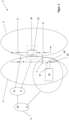
- the electronic installation device 1 shows a basic circuit arrangement for an electronic installation device 1.
- the electronic installation device 1 can preferably be connected in series with a load (not shown).
- the electronic installation device 1 comprises a load circuit 2 and a control circuit 3, which are thermally, physically and/or electrically coupled.
- the electronic installation device 1 is protected against overcurrent by a combination of two specific, coordinated protective devices.
- a first overcurrent protection device 4 protects against a short circuit, while a second overcurrent protection device 5 protects against overload.
- the electronic installation device 1 contains a circuit-breaking element 6 in the form of a switching contact of a relay 7 with which the electrical connection of the load to a voltage supply can be switched on and off.
- the relay 7 is controlled by a control device 8 in the control circuit 3, which supplies switching commands to a coil of the relay 7.
- the load circuit 2 comprises a first overcurrent protection device 4, a resistance element 9 and the circuit breaking element 6, which are arranged in series between a power source (not shown) and an electric load.
- An overcurrent detection device 10 acts together with the control device 8 as a second overcurrent protection device 5.
- the control device 8 is arranged in the control circuit 3 and functionally connected to the circuit-breaking element 6 in the load circuit 2.
- the overcurrent detection device 10 includes a sensor element 11 in the control circuit 3, preferably a reversible electrical component in the form of a positive PTC thermistor Temperature coefficient (PTC), and the resistance element 9 in the load circuit 2, which is thermally coupled to the PTC element 11.
- PTC PTC thermistor Temperature coefficient
- the resistance element 9 runs as a galvanically isolated conductor below the PTC element 11.
- the electronic installation device 1 is at least partially implemented on a printed circuit board structure 12 and has the first overcurrent protection device 4 in the form of a fuse in the load circuit 2, which protects the device's own electrical components and conductors in the event of a short circuit.
- the melting integral of the protected components and conductor tracks is higher than the melting integral of fuse 4.
- Fuse 4 is only designed for short circuits and not for overload.
- the certified fuse 4 used is designed to minimize temperature influences and to process a tripping current. In the event of a short circuit, the load circuit 2 is permanently interrupted by the fuse 4.
- the resistance element 9 in the form of a conductor track of the load circuit is designed specifically so that it is not destroyed in the event of a short circuit and also allows the thermal energy to be detected in the event of an overload.
- the conductor track consists of two parallel conductor tracks 13 and 14 of different widths.
- the width ratio is preferably 5 to 1.
- the wide strip conductor 14 absorbs the short-circuit current, while the narrow strip conductor 13 serves to detect the overload current.
- the common melting integral of both conductor tracks 13 and 14 is higher than the melting integral of fuse 4.
- the electrical network of a house installation can supply the operating current for the electronic installation device 1 .
- the load control circuit 2 that Circuit breaking element 6 of relay 7 is closed
- the operating current flows to the load, e.g. a brushed motor with relatively high current for a blind control.
- a control power source separate from the primary power source, provides control power for the control circuit 3.
- the control current flows to a coil of the relay 7 and normally causes the circuit breaker element 6 to close, thereby closing the load circuit 2.
- the electronic installation device 1 is in a low-temperature, low-resistance state.
- a fault current is a level of current that damages one of the components of an electrical circuit.
- the current rises very quickly and causes the fusible conductor in the first overcurrent protection device 4 to melt, as a result of which the flow of current is permanently interrupted. Since the common melting integral of the two conductor tracks 13 and 14 of the resistance element 9 is higher, there is no damage at this point.
- the narrow strip conductor 13 is not destroyed in the process, since when there is a high current flow in the event of a short circuit, the current uses the path of least resistance via the sufficiently dimensioned wide strip conductor 14 .
- the safety fuse 4 does not trigger in the event of an overload in the range between the short-circuit current (fuse tripping current) and the rated current of the electronic installation device 1 .
- the current through the resistance element 9 rises quickly but comparatively little, with the ambient temperature of the narrow conductor track 13 in particular rising excessively and being maintained for longer than the normal operating time.
- the PTC element 11 is "triggered” by the ambient temperature of the narrow conductor line 13, ie into a high temperature and high resistance state converted so that the current is significantly reduced.
- the change in the resistance and current values is "communicated” to the control device 8 .
- the PTC element 11 forms a voltage divider with a resistor 15, the changing voltage of which is read into a microcontroller 16 and processed.
- the relay 7 connected to an output 17 of the microcontroller 16 via a transistor 18 is switched off and the corresponding functionally coupled circuit breaker element 6 opens and the load is thus also switched off.
- Different operating modes can be set on the microcontroller 16 . For example, it can be specified whether the load should be switched on again automatically after a while, or only after a new switch-on command or after the interruption of load circuit 2 has been reset. The tripping characteristic can also be selected.
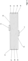
- a possible printed circuit board structure 12 of the electronic installation device 1 which consists of one or more substrate layers 19 to 22, a dielectric core layer with electrical components arranged on one or both sides and/or have conductor tracks.
- the two overcurrent protection devices 4 and 5 are formed at least partially on the two outer main surfaces 23 and 24 of the circuit board structure 12 .
- On the lower substrate layer 19 is the first overcurrent protection device, in the form of a safety fuse 4, and on the upper substrate layer 22 is at least the sensor element 11 of the second overcurrent protection device 5, in the form of a PTC element.
- Conductor tracks 13 and 14 of resistance element 9, which are electrically connected in parallel, are arranged below the PTC element.
- the correspondingly structured conductor track is arranged in different substrate layers of the circuit board structure 12 .
- the tapered conductive line 13 is arranged in the substrate layer 20 while the wide conductive line 14 is arranged in the substrate layer 21 .
- the two conductor tracks 13 and 14 are directly connected by conductive vias.
- the narrow strip conductor 13 is arranged close to the surface in the layer 20 in order to enable the use of a PTC element 11 on the surface (SMD technology).
- the PTC element 11 on the substrate layer 19 is in thermal contact with the substrate layer 20 just above the surface of the tapered conductor track 13 so that heat is generated there due to an overcurrent condition and is effectively transferred to the PTC element 11, so that as before explains a control signal is generated.
- the layers of circuit board assembly 12 are as thin as is structurally practical.
- the dielectric material forming the substrate can be a thin polyester material or other suitable thin flexible substrate.
- a thin but relatively rigid glass fiber reinforced resin substrate may also be used.
- the patterning of the copper layers can be accomplished by conventional photoresist and chemical etching techniques known to those skilled in the art.
- the various layers of the circuit board assembly are used to maximize the area of the Conductor tracks to withstand a short-circuit current.
- layers 25 to 27 of FR4 of a common height are used as the standard dielectric.
- Suitable PTC elements 11 consist of a PTC conductive polymer, ie a composition comprising an organic polymer and a particulate conductive filler and/or a conductive inorganic filler.
Landscapes
- Physics & Mathematics (AREA)
- Electromagnetism (AREA)
- Emergency Protection Circuit Devices (AREA)
- Charge And Discharge Circuits For Batteries Or The Like (AREA)
Applications Claiming Priority (2)
| Application Number | Priority Date | Filing Date | Title |
|---|---|---|---|
| DE102019116789.2A DE102019116789A1 (de) | 2019-06-21 | 2019-06-21 | Elektronisches Installationsgerät |
| PCT/EP2020/066404 WO2020254213A1 (de) | 2019-06-21 | 2020-06-12 | Elektronisches installationsgerät |
Publications (2)
| Publication Number | Publication Date |
|---|---|
| EP3970176A1 EP3970176A1 (de) | 2022-03-23 |
| EP3970176B1 true EP3970176B1 (de) | 2023-08-30 |
Family
ID=71094369
Family Applications (1)
| Application Number | Title | Priority Date | Filing Date |
|---|---|---|---|
| EP20732882.4A Active EP3970176B1 (de) | 2019-06-21 | 2020-06-12 | Elektronisches installationsgerät |
Country Status (9)
| Country | Link |
|---|---|
| US (1) | US12046892B2 (da) |
| EP (1) | EP3970176B1 (da) |
| CN (1) | CN114175204B (da) |
| AU (1) | AU2020294848B2 (da) |
| DE (1) | DE102019116789A1 (da) |
| DK (1) | DK3970176T3 (da) |
| ES (1) | ES2966689T3 (da) |
| FI (1) | FI3970176T3 (da) |
| WO (1) | WO2020254213A1 (da) |
Families Citing this family (1)
| Publication number | Priority date | Publication date | Assignee | Title |
|---|---|---|---|---|
| CN113258530B (zh) * | 2021-06-07 | 2022-02-11 | 深圳瑞能电气设备有限公司 | 一种具备过流保护和告警功能的交流双电切换装置 |
Family Cites Families (12)
| Publication number | Priority date | Publication date | Assignee | Title |
|---|---|---|---|---|
| DE3013016A1 (de) * | 1980-04-03 | 1981-10-08 | Brown, Boveri & Cie Ag, 6800 Mannheim | Ausloesesystem eines selbstschalters zur unterbrechung eines stromkreises |
| EP0096834A3 (de) * | 1982-06-11 | 1985-10-30 | Wickmann-Werke GmbH | Schutzschaltung, insbesondere für elektrische Geräte |
| SU1304127A1 (ru) | 1985-09-30 | 1987-04-15 | Научно-Производственное Объединение "Черметавтоматика" | Устройство дл дистанционного отключени выключател |
| DE4120005A1 (de) * | 1991-06-18 | 1992-12-24 | Abb Patent Gmbh | Schutzschalter |
| DE19927762A1 (de) | 1999-06-17 | 2001-01-04 | Abb Research Ltd | Neue elektrische Schalteinrichtung zum Überstromschutz |
| DE10119458B4 (de) * | 2001-04-20 | 2004-08-19 | Siemens Ag | Schaltgeräteeinheit für einen Verbraucher, insbesondere Motorstarter |
| RU2321164C1 (ru) | 2006-11-23 | 2008-03-27 | Открытое акционерное общество "Специальное конструкторско-технологическое бюро по релейной технике" (ОАО "СКТБ РТ") | Коммутатор напряжения с защитой от перегрузки по току |
| DE102006059384B4 (de) * | 2006-12-15 | 2013-02-21 | Siemens Aktiengesellschaft | Gerät mit einem Stromwandler zur Erfassung eines durch einen Stromleiter fließenden Stromes sowie Klemmen-/Stromwandler-Modul für ein derartiges Gerät |
| JP5171406B2 (ja) * | 2008-06-05 | 2013-03-27 | 矢崎総業株式会社 | 負荷回路の過電流保護装置 |
| CN106663566B (zh) * | 2014-03-07 | 2019-06-25 | 力特电子(日本)有限责任公司 | 保护设备 |
| DE102015001945A1 (de) * | 2015-02-16 | 2016-08-18 | Ellenberger & Poensgen Gmbh | Schutzschalter und Verfahren zu dessen Betrieb |
| TWI597754B (zh) * | 2016-05-20 | 2017-09-01 | 聚鼎科技股份有限公司 | 保護元件及其電路保護裝置 |
-
2019
- 2019-06-21 DE DE102019116789.2A patent/DE102019116789A1/de not_active Withdrawn
-
2020
- 2020-06-12 WO PCT/EP2020/066404 patent/WO2020254213A1/de not_active Ceased
- 2020-06-12 FI FIEP20732882.4T patent/FI3970176T3/fi active
- 2020-06-12 AU AU2020294848A patent/AU2020294848B2/en active Active
- 2020-06-12 DK DK20732882.4T patent/DK3970176T3/da active
- 2020-06-12 ES ES20732882T patent/ES2966689T3/es active Active
- 2020-06-12 US US17/619,981 patent/US12046892B2/en active Active
- 2020-06-12 EP EP20732882.4A patent/EP3970176B1/de active Active
- 2020-06-12 CN CN202080053564.5A patent/CN114175204B/zh active Active
Also Published As
| Publication number | Publication date |
|---|---|
| AU2020294848A1 (en) | 2022-01-27 |
| ES2966689T3 (es) | 2024-04-23 |
| EP3970176A1 (de) | 2022-03-23 |
| WO2020254213A1 (de) | 2020-12-24 |
| US12046892B2 (en) | 2024-07-23 |
| CN114175204B (zh) | 2025-05-13 |
| US20220360069A1 (en) | 2022-11-10 |
| DE102019116789A1 (de) | 2020-12-24 |
| FI3970176T3 (fi) | 2023-12-11 |
| CN114175204A (zh) | 2022-03-11 |
| AU2020294848B2 (en) | 2024-05-30 |
| DK3970176T3 (da) | 2023-12-04 |
Similar Documents
| Publication | Publication Date | Title |
|---|---|---|
| EP1019934B1 (de) | Schaltungsanordnung und verfahren zum betreiben eines sicherungselements | |
| DE69937860T2 (de) | Schutzschalter mit Lichtbogenfehlerschutz und PTC-Elemente zum Schutz gegen Kurzschluss und Überlastung | |
| DE602005000540T2 (de) | Überspannungs-Schutzeinrichtung | |
| DE112009004858B4 (de) | Schaltung mit einem selbstschaltenden Wärme-Schutzschalter und einem Strombegrenzungs-element für einen elektrischen Schaltkreis, sowie einen entsprechenden elektrischen Schaltkreis | |
| EP3264439B1 (de) | Schmelzleiter und überstrom-schutzeinrichtung | |
| DE68916152T3 (de) | Überstromschutzeinrichtung für elektrische Netzwerke und Apparate. | |
| WO1999033079A1 (de) | Elektrische sicherung | |
| DE2724269C2 (de) | Überlastungsschutz-Schaltung | |
| EP3970176B1 (de) | Elektronisches installationsgerät | |
| DE69811721T2 (de) | Stromversorgungsnetz mit einer vorrichtung zum vorladen und einer kapazitiven last | |
| DE102009031138B4 (de) | Schalteinrichtung | |
| DE10325761A1 (de) | Vorwiderstandsbaugruppe für einen Elektromotor und Schaltungsanordnung mit ein er Vorwiderstandsbaugruppe zum Betreiben eines Elektromotors sowie Verwendung einer Vorwiderstandsbaugruppe | |
| DE3544647A1 (de) | Fehlerstromschalter | |
| EP3347911B1 (de) | Laststromtragende sicherung mit internem schaltelement | |
| DE102018129679B4 (de) | Überspannungsschutzvorrichtung mit thermischer Überlastschutzvorrichtung | |
| DE102021126909A1 (de) | Trennschaltanordnung zur absicherung eines fahrzeug-bordnetzes | |
| RU2815454C2 (ru) | Электронный установочный прибор | |
| DE19754981A1 (de) | Elektronischer Installationsschalter | |
| DE3706184C2 (da) | ||
| DE19833224B4 (de) | Schaltungsanordnung zum Schutz einer elektrischen Last | |
| EP1361636A1 (de) | Schutzschalter für eine Kabeltrommel | |
| EP2837075B1 (de) | Vorrichtung zum schutz eines verbrauchers | |
| DE19754415A1 (de) | Schutzschaltung | |
| DE102022202971A1 (de) | Schaltvorrichtung mit MEMS-Relais | |
| EP4105960A1 (de) | Sicherungseinrichtung für ein elektrisches energieversorgungsnetz |
Legal Events
| Date | Code | Title | Description |
|---|---|---|---|
| STAA | Information on the status of an ep patent application or granted ep patent |
Free format text: STATUS: UNKNOWN |
|
| STAA | Information on the status of an ep patent application or granted ep patent |
Free format text: STATUS: THE INTERNATIONAL PUBLICATION HAS BEEN MADE |
|
| PUAI | Public reference made under article 153(3) epc to a published international application that has entered the european phase |
Free format text: ORIGINAL CODE: 0009012 |
|
| STAA | Information on the status of an ep patent application or granted ep patent |
Free format text: STATUS: REQUEST FOR EXAMINATION WAS MADE |
|
| 17P | Request for examination filed |
Effective date: 20211213 |
|
| AK | Designated contracting states |
Kind code of ref document: A1 Designated state(s): AL AT BE BG CH CY CZ DE DK EE ES FI FR GB GR HR HU IE IS IT LI LT LU LV MC MK MT NL NO PL PT RO RS SE SI SK SM TR |
|
| DAV | Request for validation of the european patent (deleted) | ||
| DAX | Request for extension of the european patent (deleted) | ||
| GRAP | Despatch of communication of intention to grant a patent |
Free format text: ORIGINAL CODE: EPIDOSNIGR1 |
|
| STAA | Information on the status of an ep patent application or granted ep patent |
Free format text: STATUS: GRANT OF PATENT IS INTENDED |
|
| INTG | Intention to grant announced |
Effective date: 20230519 |
|
| GRAS | Grant fee paid |
Free format text: ORIGINAL CODE: EPIDOSNIGR3 |
|
| GRAA | (expected) grant |
Free format text: ORIGINAL CODE: 0009210 |
|
| STAA | Information on the status of an ep patent application or granted ep patent |
Free format text: STATUS: THE PATENT HAS BEEN GRANTED |
|
| AK | Designated contracting states |
Kind code of ref document: B1 Designated state(s): AL AT BE BG CH CY CZ DE DK EE ES FI FR GB GR HR HU IE IS IT LI LT LU LV MC MK MT NL NO PL PT RO RS SE SI SK SM TR |
|
| REG | Reference to a national code |
Ref country code: GB Ref legal event code: FG4D Free format text: NOT ENGLISH |
|
| REG | Reference to a national code |
Ref country code: CH Ref legal event code: EP |
|
| REG | Reference to a national code |
Ref country code: DE Ref legal event code: R096 Ref document number: 502020004997 Country of ref document: DE |
|
| REG | Reference to a national code |
Ref country code: IE Ref legal event code: FG4D Free format text: LANGUAGE OF EP DOCUMENT: GERMAN |
|
| REG | Reference to a national code |
Ref country code: DK Ref legal event code: T3 Effective date: 20231130 Ref country code: NO Ref legal event code: T2 Effective date: 20230830 |
|
| REG | Reference to a national code |
Ref country code: FI Ref legal event code: FGE |
|
| REG | Reference to a national code |
Ref country code: NL Ref legal event code: FP |
|
| REG | Reference to a national code |
Ref country code: LT Ref legal event code: MG9D Ref country code: SE Ref legal event code: TRGR |
|
| PG25 | Lapsed in a contracting state [announced via postgrant information from national office to epo] |
Ref country code: GR Free format text: LAPSE BECAUSE OF FAILURE TO SUBMIT A TRANSLATION OF THE DESCRIPTION OR TO PAY THE FEE WITHIN THE PRESCRIBED TIME-LIMIT Effective date: 20231201 |
|
| PG25 | Lapsed in a contracting state [announced via postgrant information from national office to epo] |
Ref country code: IS Free format text: LAPSE BECAUSE OF FAILURE TO SUBMIT A TRANSLATION OF THE DESCRIPTION OR TO PAY THE FEE WITHIN THE PRESCRIBED TIME-LIMIT Effective date: 20231230 |
|
| PG25 | Lapsed in a contracting state [announced via postgrant information from national office to epo] |
Ref country code: RS Free format text: LAPSE BECAUSE OF FAILURE TO SUBMIT A TRANSLATION OF THE DESCRIPTION OR TO PAY THE FEE WITHIN THE PRESCRIBED TIME-LIMIT Effective date: 20230830 Ref country code: LV Free format text: LAPSE BECAUSE OF FAILURE TO SUBMIT A TRANSLATION OF THE DESCRIPTION OR TO PAY THE FEE WITHIN THE PRESCRIBED TIME-LIMIT Effective date: 20230830 Ref country code: LT Free format text: LAPSE BECAUSE OF FAILURE TO SUBMIT A TRANSLATION OF THE DESCRIPTION OR TO PAY THE FEE WITHIN THE PRESCRIBED TIME-LIMIT Effective date: 20230830 Ref country code: IS Free format text: LAPSE BECAUSE OF FAILURE TO SUBMIT A TRANSLATION OF THE DESCRIPTION OR TO PAY THE FEE WITHIN THE PRESCRIBED TIME-LIMIT Effective date: 20231230 Ref country code: HR Free format text: LAPSE BECAUSE OF FAILURE TO SUBMIT A TRANSLATION OF THE DESCRIPTION OR TO PAY THE FEE WITHIN THE PRESCRIBED TIME-LIMIT Effective date: 20230830 Ref country code: GR Free format text: LAPSE BECAUSE OF FAILURE TO SUBMIT A TRANSLATION OF THE DESCRIPTION OR TO PAY THE FEE WITHIN THE PRESCRIBED TIME-LIMIT Effective date: 20231201 |
|
| PG25 | Lapsed in a contracting state [announced via postgrant information from national office to epo] |
Ref country code: PL Free format text: LAPSE BECAUSE OF FAILURE TO SUBMIT A TRANSLATION OF THE DESCRIPTION OR TO PAY THE FEE WITHIN THE PRESCRIBED TIME-LIMIT Effective date: 20230830 |
|
| REG | Reference to a national code |
Ref country code: ES Ref legal event code: FG2A Ref document number: 2966689 Country of ref document: ES Kind code of ref document: T3 Effective date: 20240423 |
|
| PG25 | Lapsed in a contracting state [announced via postgrant information from national office to epo] |
Ref country code: SM Free format text: LAPSE BECAUSE OF FAILURE TO SUBMIT A TRANSLATION OF THE DESCRIPTION OR TO PAY THE FEE WITHIN THE PRESCRIBED TIME-LIMIT Effective date: 20230830 Ref country code: RO Free format text: LAPSE BECAUSE OF FAILURE TO SUBMIT A TRANSLATION OF THE DESCRIPTION OR TO PAY THE FEE WITHIN THE PRESCRIBED TIME-LIMIT Effective date: 20230830 Ref country code: EE Free format text: LAPSE BECAUSE OF FAILURE TO SUBMIT A TRANSLATION OF THE DESCRIPTION OR TO PAY THE FEE WITHIN THE PRESCRIBED TIME-LIMIT Effective date: 20230830 Ref country code: CZ Free format text: LAPSE BECAUSE OF FAILURE TO SUBMIT A TRANSLATION OF THE DESCRIPTION OR TO PAY THE FEE WITHIN THE PRESCRIBED TIME-LIMIT Effective date: 20230830 Ref country code: SK Free format text: LAPSE BECAUSE OF FAILURE TO SUBMIT A TRANSLATION OF THE DESCRIPTION OR TO PAY THE FEE WITHIN THE PRESCRIBED TIME-LIMIT Effective date: 20230830 Ref country code: PT Free format text: LAPSE BECAUSE OF FAILURE TO SUBMIT A TRANSLATION OF THE DESCRIPTION OR TO PAY THE FEE WITHIN THE PRESCRIBED TIME-LIMIT Effective date: 20240102 |
|
| REG | Reference to a national code |
Ref country code: DE Ref legal event code: R097 Ref document number: 502020004997 Country of ref document: DE |
|
| PLBE | No opposition filed within time limit |
Free format text: ORIGINAL CODE: 0009261 |
|
| STAA | Information on the status of an ep patent application or granted ep patent |
Free format text: STATUS: NO OPPOSITION FILED WITHIN TIME LIMIT |
|
| PG25 | Lapsed in a contracting state [announced via postgrant information from national office to epo] |
Ref country code: SI Free format text: LAPSE BECAUSE OF FAILURE TO SUBMIT A TRANSLATION OF THE DESCRIPTION OR TO PAY THE FEE WITHIN THE PRESCRIBED TIME-LIMIT Effective date: 20230830 |
|
| 26N | No opposition filed |
Effective date: 20240603 |
|
| PG25 | Lapsed in a contracting state [announced via postgrant information from national office to epo] |
Ref country code: BG Free format text: LAPSE BECAUSE OF FAILURE TO SUBMIT A TRANSLATION OF THE DESCRIPTION OR TO PAY THE FEE WITHIN THE PRESCRIBED TIME-LIMIT Effective date: 20230830 |
|
| PG25 | Lapsed in a contracting state [announced via postgrant information from national office to epo] |
Ref country code: BG Free format text: LAPSE BECAUSE OF FAILURE TO SUBMIT A TRANSLATION OF THE DESCRIPTION OR TO PAY THE FEE WITHIN THE PRESCRIBED TIME-LIMIT Effective date: 20230830 |
|
| PG25 | Lapsed in a contracting state [announced via postgrant information from national office to epo] |
Ref country code: MC Free format text: LAPSE BECAUSE OF FAILURE TO SUBMIT A TRANSLATION OF THE DESCRIPTION OR TO PAY THE FEE WITHIN THE PRESCRIBED TIME-LIMIT Effective date: 20230830 |
|
| PG25 | Lapsed in a contracting state [announced via postgrant information from national office to epo] |
Ref country code: LU Free format text: LAPSE BECAUSE OF NON-PAYMENT OF DUE FEES Effective date: 20240612 |
|
| PG25 | Lapsed in a contracting state [announced via postgrant information from national office to epo] |
Ref country code: IE Free format text: LAPSE BECAUSE OF NON-PAYMENT OF DUE FEES Effective date: 20240612 |
|
| PG25 | Lapsed in a contracting state [announced via postgrant information from national office to epo] |
Ref country code: BE Free format text: LAPSE BECAUSE OF NON-PAYMENT OF DUE FEES Effective date: 20240630 |
|
| REG | Reference to a national code |
Ref country code: BE Ref legal event code: MM Effective date: 20240630 |
|
| PGFP | Annual fee paid to national office [announced via postgrant information from national office to epo] |
Ref country code: NL Payment date: 20250516 Year of fee payment: 6 |
|
| PGFP | Annual fee paid to national office [announced via postgrant information from national office to epo] |
Ref country code: FI Payment date: 20250620 Year of fee payment: 6 |
|
| PGFP | Annual fee paid to national office [announced via postgrant information from national office to epo] |
Ref country code: DE Payment date: 20250429 Year of fee payment: 6 |
|
| PGFP | Annual fee paid to national office [announced via postgrant information from national office to epo] |
Ref country code: GB Payment date: 20250501 Year of fee payment: 6 Ref country code: DK Payment date: 20250618 Year of fee payment: 6 |
|
| PGFP | Annual fee paid to national office [announced via postgrant information from national office to epo] |
Ref country code: NO Payment date: 20250610 Year of fee payment: 6 |
|
| PGFP | Annual fee paid to national office [announced via postgrant information from national office to epo] |
Ref country code: IT Payment date: 20250522 Year of fee payment: 6 |
|
| PGFP | Annual fee paid to national office [announced via postgrant information from national office to epo] |
Ref country code: FR Payment date: 20250508 Year of fee payment: 6 |
|
| PGFP | Annual fee paid to national office [announced via postgrant information from national office to epo] |
Ref country code: AT Payment date: 20250528 Year of fee payment: 6 |
|
| PGFP | Annual fee paid to national office [announced via postgrant information from national office to epo] |
Ref country code: SE Payment date: 20250514 Year of fee payment: 6 |
|
| PGFP | Annual fee paid to national office [announced via postgrant information from national office to epo] |
Ref country code: ES Payment date: 20250702 Year of fee payment: 6 |
|
| PGFP | Annual fee paid to national office [announced via postgrant information from national office to epo] |
Ref country code: CH Payment date: 20250701 Year of fee payment: 6 |
|
| PG25 | Lapsed in a contracting state [announced via postgrant information from national office to epo] |
Ref country code: CY Free format text: LAPSE BECAUSE OF FAILURE TO SUBMIT A TRANSLATION OF THE DESCRIPTION OR TO PAY THE FEE WITHIN THE PRESCRIBED TIME-LIMIT; INVALID AB INITIO Effective date: 20200612 |
|
| PG25 | Lapsed in a contracting state [announced via postgrant information from national office to epo] |
Ref country code: HU Free format text: LAPSE BECAUSE OF FAILURE TO SUBMIT A TRANSLATION OF THE DESCRIPTION OR TO PAY THE FEE WITHIN THE PRESCRIBED TIME-LIMIT; INVALID AB INITIO Effective date: 20200612 |