EP3971991A1 - Transistor mesfet/hemt à grille empilée éliminant le courant de fuite de grille et fournissant un transistor normalement bloqué - Google Patents
Transistor mesfet/hemt à grille empilée éliminant le courant de fuite de grille et fournissant un transistor normalement bloqué Download PDFInfo
- Publication number
- EP3971991A1 EP3971991A1 EP20196868.2A EP20196868A EP3971991A1 EP 3971991 A1 EP3971991 A1 EP 3971991A1 EP 20196868 A EP20196868 A EP 20196868A EP 3971991 A1 EP3971991 A1 EP 3971991A1
- Authority
- EP
- European Patent Office
- Prior art keywords
- metal
- semiconductor
- layer
- gate
- depletion region
- Prior art date
- Legal status (The legal status is an assumption and is not a legal conclusion. Google has not performed a legal analysis and makes no representation as to the accuracy of the status listed.)
- Withdrawn
Links
Images

Classifications
-
- H—ELECTRICITY
- H10—SEMICONDUCTOR DEVICES; ELECTRIC SOLID-STATE DEVICES NOT OTHERWISE PROVIDED FOR
- H10D—INORGANIC ELECTRIC SEMICONDUCTOR DEVICES
- H10D64/00—Electrodes of devices having potential barriers
- H10D64/01—Manufacture or treatment
-
- H—ELECTRICITY
- H10—SEMICONDUCTOR DEVICES; ELECTRIC SOLID-STATE DEVICES NOT OTHERWISE PROVIDED FOR
- H10D—INORGANIC ELECTRIC SEMICONDUCTOR DEVICES
- H10D30/00—Field-effect transistors [FET]
- H10D30/40—FETs having zero-dimensional [0D], one-dimensional [1D] or two-dimensional [2D] charge carrier gas channels
- H10D30/47—FETs having zero-dimensional [0D], one-dimensional [1D] or two-dimensional [2D] charge carrier gas channels having two-dimensional [2D] charge carrier gas channels, e.g. nanoribbon FETs or high electron mobility transistors [HEMT]
- H10D30/471—High electron mobility transistors [HEMT] or high hole mobility transistors [HHMT]
-
- H—ELECTRICITY
- H10—SEMICONDUCTOR DEVICES; ELECTRIC SOLID-STATE DEVICES NOT OTHERWISE PROVIDED FOR
- H10D—INORGANIC ELECTRIC SEMICONDUCTOR DEVICES
- H10D30/00—Field-effect transistors [FET]
- H10D30/80—FETs having rectifying junction gate electrodes
- H10D30/87—FETs having Schottky gate electrodes, e.g. metal-semiconductor FETs [MESFET]
- H10D30/875—FETs having Schottky gate electrodes, e.g. metal-semiconductor FETs [MESFET] having thin-film semiconductor bodies
-
- H—ELECTRICITY
- H10—SEMICONDUCTOR DEVICES; ELECTRIC SOLID-STATE DEVICES NOT OTHERWISE PROVIDED FOR
- H10D—INORGANIC ELECTRIC SEMICONDUCTOR DEVICES
- H10D30/00—Field-effect transistors [FET]
- H10D30/40—FETs having zero-dimensional [0D], one-dimensional [1D] or two-dimensional [2D] charge carrier gas channels
- H10D30/47—FETs having zero-dimensional [0D], one-dimensional [1D] or two-dimensional [2D] charge carrier gas channels having two-dimensional [2D] charge carrier gas channels, e.g. nanoribbon FETs or high electron mobility transistors [HEMT]
- H10D30/481—FETs having two-dimensional material channels, e.g. transition metal dichalcogenide [TMD] FETs
-
- H—ELECTRICITY
- H10—SEMICONDUCTOR DEVICES; ELECTRIC SOLID-STATE DEVICES NOT OTHERWISE PROVIDED FOR
- H10D—INORGANIC ELECTRIC SEMICONDUCTOR DEVICES
- H10D30/00—Field-effect transistors [FET]
- H10D30/60—Insulated-gate field-effect transistors [IGFET]
- H10D30/611—Insulated-gate field-effect transistors [IGFET] having multiple independently-addressable gate electrodes influencing the same channel
- H10D30/615—Insulated-gate field-effect transistors [IGFET] having multiple independently-addressable gate electrodes influencing the same channel comprising a MOS gate electrode and at least one non-MOS gate electrode
-
- H—ELECTRICITY
- H10—SEMICONDUCTOR DEVICES; ELECTRIC SOLID-STATE DEVICES NOT OTHERWISE PROVIDED FOR
- H10D—INORGANIC ELECTRIC SEMICONDUCTOR DEVICES
- H10D30/00—Field-effect transistors [FET]
- H10D30/80—FETs having rectifying junction gate electrodes
- H10D30/87—FETs having Schottky gate electrodes, e.g. metal-semiconductor FETs [MESFET]
- H10D30/873—FETs having Schottky gate electrodes, e.g. metal-semiconductor FETs [MESFET] having multiple gate electrodes
-
- H—ELECTRICITY
- H10—SEMICONDUCTOR DEVICES; ELECTRIC SOLID-STATE DEVICES NOT OTHERWISE PROVIDED FOR
- H10D—INORGANIC ELECTRIC SEMICONDUCTOR DEVICES
- H10D62/00—Semiconductor bodies, or regions thereof, of devices having potential barriers
- H10D62/80—Semiconductor bodies, or regions thereof, of devices having potential barriers characterised by the materials
- H10D62/881—Semiconductor bodies, or regions thereof, of devices having potential barriers characterised by the materials being a two-dimensional material
- H10D62/882—Graphene
-
- H—ELECTRICITY
- H10—SEMICONDUCTOR DEVICES; ELECTRIC SOLID-STATE DEVICES NOT OTHERWISE PROVIDED FOR
- H10D—INORGANIC ELECTRIC SEMICONDUCTOR DEVICES
- H10D64/00—Electrodes of devices having potential barriers
- H10D64/20—Electrodes characterised by their shapes, relative sizes or dispositions
- H10D64/27—Electrodes not carrying the current to be rectified, amplified, oscillated or switched, e.g. gates
- H10D64/311—Gate electrodes for field-effect devices
- H10D64/411—Gate electrodes for field-effect devices for FETs
Definitions
- This invention relates to eliminating the direct connection between the metal gate of a metal semiconductor field effect transistor (MESFET) and/or high electron mobility transistor (HEMT) to its semiconductor body.
- this invention provides for elimination of reverse bias leakage current of the gate Schottky junction and also provides for a normally OFF transistor.
- MESFET metal semiconductor field effect transistor
- HEMT high electron mobility transistor
- This invention provides for elimination of reverse bias leakage current of the gate Schottky junction and also provides for a normally OFF transistor.
- the top metal layer provides an isolated connection to the bottom metal gate and affects it electrostatically.
- Application of voltage to the top metal induces charges in the bottom layer and modulates the depletion region. Both positive and negative voltages can be applied to the gate to either increase or decrease the size of the depletion region.
- normally OFF HEMT and MESFET transistors can be obtained by choosing the work function of the lower metal layer such that the depletion region it creates completely fills the semiconductor layer or by applying a reverse bias voltage to the lower metal layer.
- the device would be normally off and when a forward bias voltage is applied to the isolated metal the depletion region shrinks, due to the charges induced in the bottom metal, and as a result current starts to flow through the body of the device.
- Both normally ON and OFF devices can be obtained and can work in tandem to provide for digital circuits.
- This invention is applicable to all types of MESFET transistors, to which HEMT family belongs, and it also applies to all types of semiconductor materials be it elemental such as Si and Ge or hetero-junction layers of GaAs, GaN or other families of compound semiconductors or 2D materials such as Graphene, etc.
- the insulating layer created on top of the lower metal layer can be obtained via a number of well-known processes in the literature such as oxidation, nitride alloy creation, incorporation of various compounds or deposition of different insulating layers with various methods.
- a Metal Semiconductor Field Effect Transistor (MESFET) device comprises a layer of semiconductor with two connections for flow of electrical current, being termed source and drain. Between the source and drain a metal connection to the semiconductor such that a Schottky contact is created, this metal connection being termed gate. A depletion region is formed due to the Schottky contact, the depletion region extending into the semiconductor. An insulating layer is formed over the metal gate of this MESFET and another metal layer is deposited over the insulator, wherein a gate voltage is applied to the second metal layer while the insulating layer is thick enough to prevent any leakage current from the second to the first metal gate layer.
- This feature can be added to any and all MESFETs of various designs and materials including High Electron Mobility Transistors (HEMT).
- HEMT High Electron Mobility Transistors
- the MESFET is a High Electron Mobility Transistors (HEMT).
- HEMT High Electron Mobility Transistors
- the insulating layer can be created by allowing the top surface of the first metal layer make an insulating material with a gas inside a vacuum chamber or via chemical processes. In an alternative embodiment the insulating layer is created via deposition of an entirely new material.
- the first metal can be comprised of different metal layers itself such that the topmost layer makes a more appropriate surface for insulator creation.
- the first metal can be chosen such that its work function and physical properties, in conjunction with the semiconductor properties, result in a depletion region width less than the thickness of the semiconductor material. Changes in semiconductor thickness or impurity doping of different types to create such a condition is within the scope of this invention.
- the first metal such that its work function and physical properties, in conjunction with the semiconductor properties, result in a depletion region that covers the whole semiconductor thickness and turns it off. Changes in semiconductor thickness or impurity doping of different types to create such a condition is within the scope of this invention.
- the first metal can be connected to an independent bias voltage in order to extend the depletion region all the way through the semiconductor layer and turn the device off under normal circumstances.
- a voltage can be applied to the top gate metal such that the Schottky junction is reverse biased and the width of the depletion region increase with such polarity of voltage. This is similar to conventional MESFET operation but without the leakage current.
- the voltage can be applied to the top gate metal such that the Schottky junction is forward biased and the width of the depletion region decrease with such polarity of the voltage.
- the inventive device can be used in any high frequency and/or high power combination that regular HEMT transistors are being used with the added features of eliminating gate leakage current or obtaining normally OFF HEMT transistor.
- the semiconductor layer can be a 2D material such as Graphene, etc.
- High electron mobility transistors fall under the broad category of junction field effect transistors (JFET).
- JFET junction field effect transistors
- HEMTs are basically MESFETs whose semiconductor body is made of several layers of varying doping and band gap material that can be grown on top of each other with high quality and precision.
- One of these layers is intrinsic where electrons can achieve high motilities, not achievable in regular transistors. This high mobility layer is the essence of HEMT transistor operational advantage.
- HEMTs are extensively used in high frequency and high power applications. These range from cellular communications and radar to power converters in renewable energy applications. Most commonly used HEMTs are based on GaAs, GaN and Inp family of materials. This invention applies to all families of materials used in HEMTs as well as MESFETs.
- HEMTs and MESFETs use the metal side of a Schottky junction as their control or gate terminal, care must be taken to assure the junction remains reverse biased during device's operation. However, in reverse bias there is still leakage current from gate into the semiconductor, which limits the power delivery and operational temperature of the device.
- MOSFET type structures have been proposed such as provided in US 2017/0294529A1 "High electron mobility transistor (HEMT) device” by Edward A. Beam, et al or US 2006/0138456 A1 "Insulating gate ALGAN/GAN HEMT" by Primit Parikh, et al.
- MESFET devices are normally ON, which means if there is no voltage applied to the gate, current easily passes through the device.
- this invention provides a new concept for obtaining transistors using two-dimensional materials such as Graphene.
- the semiconductor can be replaced by any of the two-dimensional materials, which can provide Schottky contact with a metal.
- the Schottky contact modulates the carrier density inside the two-dimensional material.
- the source and drain therefore are of the same doping as the material itself, which greatly helps with processing and utility of these materials.
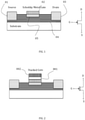
- a MESFET according to the invention comprises a substrate, which could be an intrinsic semiconductor or an appropriate insulator. There is a semiconductor 04 layer on top of the substrate, which could be an elemental semiconductor such as Si or hetero-junction layers of GaAs or GaN, etc, which include layers for creating a high electron mobility region. Electrical current passes from terminals 01 to 03 through the semiconductor. Gate metallic layer 02 creates the depletion region 05 whose depth can be changed by the gate voltage. To the right the symbol for n channel MESFET is provided. A p channel device would have its gate arrow pointing in the opposite direction coming out of the device.
- an insulating layer 001 is created over the metal. On top of that another metal layer 002 is deposited. To the right a circuit representation is presented for clarity in which the stacked gate is represented by two separated lines as the gate connection. Again the semiconductor material could be elemental, compound or 2D material.
- FIG. 3 shows the depletion mode or normally OFF version of the invention.
- the metal contact 001 has been chosen such that its work function, with respect to the semiconductor properties, provides a depletion region 002 that fills the whole semiconductor thickness. This provides for a normally OFF device.
- the area between the two metal gates is blackened. Again for p channel devices the direction of the arrow is reversed at the gate connection.
- FIG.4 shows a different way of obtaining a normally OFF transistor without changing the fist metal gate layer's work function.
- This metal is designated by 00001 and is similar to FIG. 2 and creates a depletion region that does not extend all the way into the semiconductor. However application of a bias voltage extends the depletion region all the way and turns the device off. Now applying voltage to the top metal can turn the device on.
- a reverse bias voltage applied to the gate would increase the depth of the depletion region in FIG. 1 and constricts carrier movement (electron or hole currents) from the source to the drain.
- the same event can occur for the structure of FIG. 2 if the voltage is applied to the top metal. This is so because the charges accumulated on the top metal induce opposite charges on the top surface of the bottom metal layer and like charges at its bottom surface. This charge in turn affects the depth of the depletion region exactly the same way as when the charges are created directly by the gate voltage in regular MESFETs.
- the important result is that the depletion region width can be controlled without current passing from the gate into the semiconductor. This means that the leakage current from the gate to the semiconductor can be essentially eliminated.
- the depletion region can either be extended or narrowed depending on the polarity of the voltage. In the latter case it allows us to choose the bottom metal layer such that its associated depletion region extends all the way down through the semiconductor reaching the insulating layer at the bottom. This completely impedes flow of carriers from source to the drain. This means that the transistor is normally OFF and is said to operate in depletion mode.
- the size of the depletion region is a function of the relative difference between the work functions of the metal and semiconductor and its relation to its electron affinity. It is also related to the doping level of the semiconductor material. These can be tailored such that the depletion region extends all the way down. To obtain very fast devices without the need for high mobility transistors one can use Graphene or other 2D materials with very large mobility as the semiconductor material.
Landscapes
- Junction Field-Effect Transistors (AREA)
Priority Applications (5)
| Application Number | Priority Date | Filing Date | Title |
|---|---|---|---|
| EP20196868.2A EP3971991A1 (fr) | 2020-09-18 | 2020-09-18 | Transistor mesfet/hemt à grille empilée éliminant le courant de fuite de grille et fournissant un transistor normalement bloqué |
| CN202180063691.8A CN116195069A (zh) | 2020-09-18 | 2021-09-13 | 具有叠层栅极接触件的常关型mesfet器件 |
| US18/245,838 US20240038869A1 (en) | 2020-09-18 | 2021-09-13 | Normally-off mesfet device with stacked gate contact |
| EP21777477.7A EP4214755A1 (fr) | 2020-09-18 | 2021-09-13 | Dispositif mesfet normalement bloqué à contact de grille empilé |
| PCT/EP2021/075056 WO2022058269A1 (fr) | 2020-09-18 | 2021-09-13 | Dispositif mesfet normalement bloqué à contact de grille empilé |
Applications Claiming Priority (1)
| Application Number | Priority Date | Filing Date | Title |
|---|---|---|---|
| EP20196868.2A EP3971991A1 (fr) | 2020-09-18 | 2020-09-18 | Transistor mesfet/hemt à grille empilée éliminant le courant de fuite de grille et fournissant un transistor normalement bloqué |
Publications (1)
| Publication Number | Publication Date |
|---|---|
| EP3971991A1 true EP3971991A1 (fr) | 2022-03-23 |
Family
ID=72603316
Family Applications (1)
| Application Number | Title | Priority Date | Filing Date |
|---|---|---|---|
| EP20196868.2A Withdrawn EP3971991A1 (fr) | 2020-09-18 | 2020-09-18 | Transistor mesfet/hemt à grille empilée éliminant le courant de fuite de grille et fournissant un transistor normalement bloqué |
Country Status (1)
| Country | Link |
|---|---|
| EP (1) | EP3971991A1 (fr) |
Cited By (2)
| Publication number | Priority date | Publication date | Assignee | Title |
|---|---|---|---|---|
| EP4307392A1 (fr) * | 2022-07-11 | 2024-01-17 | III-V Technologies GmbH | Dispositif jfet à contact de porte empilé |
| CN118610165A (zh) * | 2024-06-11 | 2024-09-06 | 湖北九峰山实验室 | SiC JFET晶片上外延GaN HEMT高压器件的制备方法 |
Citations (4)
| Publication number | Priority date | Publication date | Assignee | Title |
|---|---|---|---|---|
| US5274255A (en) * | 1991-08-30 | 1993-12-28 | Houssaye Paul De | Structure for providing high resolution modulation of voltage potential in the vicinity of a surface |
| US20060138456A1 (en) | 2001-07-24 | 2006-06-29 | Cree, Inc. | Insulating gate AlGaN/GaN HEMT |
| JP2012094746A (ja) * | 2010-10-28 | 2012-05-17 | New Japan Radio Co Ltd | 窒化物半導体装置およびその製造方法 |
| US20170294529A1 (en) | 2016-04-11 | 2017-10-12 | Qorvo Us, Inc. | High electron mobility transistor (hemt) device |
-
2020
- 2020-09-18 EP EP20196868.2A patent/EP3971991A1/fr not_active Withdrawn
Patent Citations (4)
| Publication number | Priority date | Publication date | Assignee | Title |
|---|---|---|---|---|
| US5274255A (en) * | 1991-08-30 | 1993-12-28 | Houssaye Paul De | Structure for providing high resolution modulation of voltage potential in the vicinity of a surface |
| US20060138456A1 (en) | 2001-07-24 | 2006-06-29 | Cree, Inc. | Insulating gate AlGaN/GaN HEMT |
| JP2012094746A (ja) * | 2010-10-28 | 2012-05-17 | New Japan Radio Co Ltd | 窒化物半導体装置およびその製造方法 |
| US20170294529A1 (en) | 2016-04-11 | 2017-10-12 | Qorvo Us, Inc. | High electron mobility transistor (hemt) device |
Non-Patent Citations (3)
| Title |
|---|
| C. A. MEAD.: "Schottky barrier gate field effect transistor", PROCEEDINGS OF THE IEEE, vol. 54, no. 2, 1966, pages 307 - 308 |
| SAITO, W.TAKADA, Y.KURAGUCHI, M.TSUDA, K.OMURA, I.: "Recessed-gate structure approach toward normally off high-Voltage AlGaN/GaN HEMT for power electronics applications", IEEE ELECTRON DEVICE LETT, vol. 53, 2006, pages 356 - 362, XP002736427, DOI: 10.1109/TED.2005.862708 |
| T. MIMURA ET AL.: "A new field-effect transistor with selectively doped GaAs/n-AlxGai-x As hetero-junctions", JPN. J. APPL. PHYS., vol. 19, no. 5, 1980, pages L225 - L227 |
Cited By (2)
| Publication number | Priority date | Publication date | Assignee | Title |
|---|---|---|---|---|
| EP4307392A1 (fr) * | 2022-07-11 | 2024-01-17 | III-V Technologies GmbH | Dispositif jfet à contact de porte empilé |
| CN118610165A (zh) * | 2024-06-11 | 2024-09-06 | 湖北九峰山实验室 | SiC JFET晶片上外延GaN HEMT高压器件的制备方法 |
Similar Documents
| Publication | Publication Date | Title |
|---|---|---|
| US7297580B2 (en) | Methods of fabricating transistors having buried p-type layers beneath the source region | |
| JP5044222B2 (ja) | Iii族窒化物電流制御デバイスおよび製造方法 | |
| CN101273458B (zh) | 增强模式ⅲ族氮化物场效应晶体管 | |
| CN108028273B (zh) | 半导体装置和制造半导体装置的方法 | |
| US7655962B2 (en) | Enhancement mode insulated gate heterostructure field-effect transistor with electrically isolated RF-enhanced source contact | |
| US20080272397A1 (en) | Semiconductor device with modulated field element | |
| US4916498A (en) | High electron mobility power transistor | |
| US20160365437A1 (en) | Electric field management for a group iii-nitride semiconductor device | |
| US10541313B2 (en) | High Electron Mobility Transistor with dual thickness barrier layer | |
| US9059239B2 (en) | Bidirectional transistor with optimized high electron mobility current | |
| US20220359738A1 (en) | Integration of p-channel and n-channel e-fet iii-v devices with optimization of device performance | |
| CN113950748A (zh) | 具有隐埋p型层的iii族氮化物高电子迁移率晶体管及其制造方法 | |
| JP4335283B2 (ja) | ソース領域下に埋込みn型およびp型領域を有するトランジスタ、およびその製造方法 | |
| JPH027532A (ja) | 積層チャネル電界効果トランジスタ | |
| US6285046B1 (en) | Controllable semiconductor structure with improved switching properties | |
| EP3971991A1 (fr) | Transistor mesfet/hemt à grille empilée éliminant le courant de fuite de grille et fournissant un transistor normalement bloqué | |
| US5101245A (en) | Field effect transistor and method for making same | |
| US5821576A (en) | Silicon carbide power field effect transistor | |
| US12575126B2 (en) | MOSFET with saturation contact and method for forming a MOSFET with saturation contact | |
| KR20240007684A (ko) | 후방 장벽 구조와 매립된 p형 층을 갖는 3족 질화물 트랜지스터 및 그 방법 | |
| TW202541616A (zh) | 氮化鎵系半導體裝置 | |
| EP4307392A1 (fr) | Dispositif jfet à contact de porte empilé | |
| US20240038869A1 (en) | Normally-off mesfet device with stacked gate contact | |
| KR20010052109A (ko) | 갈륨비소계 에피택시얼 필드 효과 트랜지스터의에피스톱층 및 그의 제조방법 | |
| WO1998035389A1 (fr) | Transistor a effet de champ metal-semiconducteur (mesfet) au carbure de silicium |
Legal Events
| Date | Code | Title | Description |
|---|---|---|---|
| PUAI | Public reference made under article 153(3) epc to a published international application that has entered the european phase |
Free format text: ORIGINAL CODE: 0009012 |
|
| STAA | Information on the status of an ep patent application or granted ep patent |
Free format text: STATUS: THE APPLICATION HAS BEEN PUBLISHED |
|
| AK | Designated contracting states |
Kind code of ref document: A1 Designated state(s): AL AT BE BG CH CY CZ DE DK EE ES FI FR GB GR HR HU IE IS IT LI LT LU LV MC MK MT NL NO PL PT RO RS SE SI SK SM TR |
|
| STAA | Information on the status of an ep patent application or granted ep patent |
Free format text: STATUS: THE APPLICATION IS DEEMED TO BE WITHDRAWN |
|
| 18D | Application deemed to be withdrawn |
Effective date: 20220924 |