EP3971992A1 - Halbleiterstruktur und verfahren zur formung davon - Google Patents
Halbleiterstruktur und verfahren zur formung davon Download PDFInfo
- Publication number
- EP3971992A1 EP3971992A1 EP19928607.1A EP19928607A EP3971992A1 EP 3971992 A1 EP3971992 A1 EP 3971992A1 EP 19928607 A EP19928607 A EP 19928607A EP 3971992 A1 EP3971992 A1 EP 3971992A1
- Authority
- EP
- European Patent Office
- Prior art keywords
- layer
- groove
- drain region
- metal silicide
- semiconductor substrate
- Prior art date
- Legal status (The legal status is an assumption and is not a legal conclusion. Google has not performed a legal analysis and makes no representation as to the accuracy of the status listed.)
- Pending
Links
Images

Classifications
-
- H—ELECTRICITY
- H10—SEMICONDUCTOR DEVICES; ELECTRIC SOLID-STATE DEVICES NOT OTHERWISE PROVIDED FOR
- H10D—INORGANIC ELECTRIC SEMICONDUCTOR DEVICES
- H10D30/00—Field-effect transistors [FET]
- H10D30/60—Insulated-gate field-effect transistors [IGFET]
- H10D30/637—Lateral IGFETs having no inversion channels, e.g. buried channel lateral IGFETs, normally-on lateral IGFETs or depletion-mode lateral IGFETs
-
- H—ELECTRICITY
- H10—SEMICONDUCTOR DEVICES; ELECTRIC SOLID-STATE DEVICES NOT OTHERWISE PROVIDED FOR
- H10D—INORGANIC ELECTRIC SEMICONDUCTOR DEVICES
- H10D30/00—Field-effect transistors [FET]
- H10D30/60—Insulated-gate field-effect transistors [IGFET]
-
- H—ELECTRICITY
- H10—SEMICONDUCTOR DEVICES; ELECTRIC SOLID-STATE DEVICES NOT OTHERWISE PROVIDED FOR
- H10D—INORGANIC ELECTRIC SEMICONDUCTOR DEVICES
- H10D64/00—Electrodes of devices having potential barriers
- H10D64/20—Electrodes characterised by their shapes, relative sizes or dispositions
- H10D64/23—Electrodes carrying the current to be rectified, amplified, oscillated or switched, e.g. sources, drains, anodes or cathodes
- H10D64/251—Source or drain electrodes for field-effect devices
- H10D64/256—Source or drain electrodes for field-effect devices for lateral devices wherein the source or drain electrodes are recessed in semiconductor bodies
-
- H—ELECTRICITY
- H10—SEMICONDUCTOR DEVICES; ELECTRIC SOLID-STATE DEVICES NOT OTHERWISE PROVIDED FOR
- H10D—INORGANIC ELECTRIC SEMICONDUCTOR DEVICES
- H10D30/00—Field-effect transistors [FET]
- H10D30/01—Manufacture or treatment
- H10D30/021—Manufacture or treatment of FETs having insulated gates [IGFET]
- H10D30/0212—Manufacture or treatment of FETs having insulated gates [IGFET] using self-aligned silicidation
-
- H—ELECTRICITY
- H10—SEMICONDUCTOR DEVICES; ELECTRIC SOLID-STATE DEVICES NOT OTHERWISE PROVIDED FOR
- H10D—INORGANIC ELECTRIC SEMICONDUCTOR DEVICES
- H10D62/00—Semiconductor bodies, or regions thereof, of devices having potential barriers
- H10D62/01—Manufacture or treatment
- H10D62/021—Forming source or drain recesses by etching e.g. recessing by etching and then refilling
-
- H—ELECTRICITY
- H10—SEMICONDUCTOR DEVICES; ELECTRIC SOLID-STATE DEVICES NOT OTHERWISE PROVIDED FOR
- H10D—INORGANIC ELECTRIC SEMICONDUCTOR DEVICES
- H10D62/00—Semiconductor bodies, or regions thereof, of devices having potential barriers
- H10D62/10—Shapes, relative sizes or dispositions of the regions of the semiconductor bodies; Shapes of the semiconductor bodies
- H10D62/113—Isolations within a component, i.e. internal isolations
- H10D62/115—Dielectric isolations, e.g. air gaps
- H10D62/116—Dielectric isolations, e.g. air gaps adjoining the input or output regions of field-effect devices, e.g. adjoining source or drain regions
-
- H—ELECTRICITY
- H10—SEMICONDUCTOR DEVICES; ELECTRIC SOLID-STATE DEVICES NOT OTHERWISE PROVIDED FOR
- H10D—INORGANIC ELECTRIC SEMICONDUCTOR DEVICES
- H10D62/00—Semiconductor bodies, or regions thereof, of devices having potential barriers
- H10D62/10—Shapes, relative sizes or dispositions of the regions of the semiconductor bodies; Shapes of the semiconductor bodies
- H10D62/124—Shapes, relative sizes or dispositions of the regions of semiconductor bodies or of junctions between the regions
- H10D62/126—Top-view geometrical layouts of the regions or the junctions
-
- H—ELECTRICITY
- H10—SEMICONDUCTOR DEVICES; ELECTRIC SOLID-STATE DEVICES NOT OTHERWISE PROVIDED FOR
- H10D—INORGANIC ELECTRIC SEMICONDUCTOR DEVICES
- H10D64/00—Electrodes of devices having potential barriers
- H10D64/01—Manufacture or treatment
-
- H—ELECTRICITY
- H10—SEMICONDUCTOR DEVICES; ELECTRIC SOLID-STATE DEVICES NOT OTHERWISE PROVIDED FOR
- H10D—INORGANIC ELECTRIC SEMICONDUCTOR DEVICES
- H10D64/00—Electrodes of devices having potential barriers
- H10D64/20—Electrodes characterised by their shapes, relative sizes or dispositions
- H10D64/205—Nanosized electrodes, e.g. nanowire electrodes
-
- H—ELECTRICITY
- H10—SEMICONDUCTOR DEVICES; ELECTRIC SOLID-STATE DEVICES NOT OTHERWISE PROVIDED FOR
- H10D—INORGANIC ELECTRIC SEMICONDUCTOR DEVICES
- H10D64/00—Electrodes of devices having potential barriers
- H10D64/20—Electrodes characterised by their shapes, relative sizes or dispositions
- H10D64/23—Electrodes carrying the current to be rectified, amplified, oscillated or switched, e.g. sources, drains, anodes or cathodes
- H10D64/251—Source or drain electrodes for field-effect devices
- H10D64/252—Source or drain electrodes for field-effect devices for vertical or pseudo-vertical devices
- H10D64/2527—Source or drain electrodes for field-effect devices for vertical or pseudo-vertical devices for vertical devices wherein the source or drain electrodes are recessed in semiconductor bodies
-
- H—ELECTRICITY
- H10—SEMICONDUCTOR DEVICES; ELECTRIC SOLID-STATE DEVICES NOT OTHERWISE PROVIDED FOR
- H10D—INORGANIC ELECTRIC SEMICONDUCTOR DEVICES
- H10D62/00—Semiconductor bodies, or regions thereof, of devices having potential barriers
- H10D62/10—Shapes, relative sizes or dispositions of the regions of the semiconductor bodies; Shapes of the semiconductor bodies
- H10D62/13—Semiconductor regions connected to electrodes carrying current to be rectified, amplified or switched, e.g. source or drain regions
- H10D62/149—Source or drain regions of field-effect devices
- H10D62/151—Source or drain regions of field-effect devices of IGFETs
-
- H—ELECTRICITY
- H10—SEMICONDUCTOR DEVICES; ELECTRIC SOLID-STATE DEVICES NOT OTHERWISE PROVIDED FOR
- H10D—INORGANIC ELECTRIC SEMICONDUCTOR DEVICES
- H10D62/00—Semiconductor bodies, or regions thereof, of devices having potential barriers
- H10D62/80—Semiconductor bodies, or regions thereof, of devices having potential barriers characterised by the materials
- H10D62/83—Semiconductor bodies, or regions thereof, of devices having potential barriers characterised by the materials being Group IV materials, e.g. B-doped Si or undoped Ge
-
- H—ELECTRICITY
- H10—SEMICONDUCTOR DEVICES; ELECTRIC SOLID-STATE DEVICES NOT OTHERWISE PROVIDED FOR
- H10D—INORGANIC ELECTRIC SEMICONDUCTOR DEVICES
- H10D62/00—Semiconductor bodies, or regions thereof, of devices having potential barriers
- H10D62/80—Semiconductor bodies, or regions thereof, of devices having potential barriers characterised by the materials
- H10D62/83—Semiconductor bodies, or regions thereof, of devices having potential barriers characterised by the materials being Group IV materials, e.g. B-doped Si or undoped Ge
- H10D62/832—Semiconductor bodies, or regions thereof, of devices having potential barriers characterised by the materials being Group IV materials, e.g. B-doped Si or undoped Ge being Group IV materials comprising two or more elements, e.g. SiGe
-
- H—ELECTRICITY
- H10—SEMICONDUCTOR DEVICES; ELECTRIC SOLID-STATE DEVICES NOT OTHERWISE PROVIDED FOR
- H10D—INORGANIC ELECTRIC SEMICONDUCTOR DEVICES
- H10D64/00—Electrodes of devices having potential barriers
- H10D64/60—Electrodes characterised by their materials
- H10D64/62—Electrodes ohmically coupled to a semiconductor
Definitions
- the present disclosure relates to the field of semiconductors, and more particularly, to a semiconductor structure and a formation method thereof.
- a contact structure on a dielectric layer to implement electrical connection between semiconductor devices is a widely used technology.
- the contact structure may be directly and electrically connected to a gate and a source/drain of a transistor, or may also be used for electrical connection between layers.
- a metal silicide layer may be formed on the surface of the gate and the source/drain of the contact structure to be formed through metal deposition and rapid annealing.
- An existing process of forming the contact structure includes following steps.
- a semiconductor substrate is provided, wherein a gate structure is formed in the semiconductor substrate, and a source/drain region is formed in the semiconductor substrate on two sides of the gate structure.
- a cobalt metal layer is deposited on a surface of the gate structure, a surface of the source/drain region, and a surface of the semiconductor substrate. Rapid thermal annealing is performed such that the cobalt metal layer reacts with silicon in the gate structure and the source/drain region to form a metal silicide. Unreacted metal is removed.
- An interlayer dielectric layer is formed on a surface of the metal silicide and the surface of the gate structure. The interlayer dielectric layer is etched to form, in the dielectric layer, a contact hole exposing the surface of the metal silicide. A metal is filled in the contact hole to form a metal plug.
- One technical problem to be solved in the present disclosure is how to reduce leakage current between a semiconductor substrate and a connection structure such as a metal plug and a metal silicide layer.
- Various embodiments provide a semiconductor structure, including:
- the contact structure further includes a buffer layer, and the buffer layer covers the insulating layer and correspondingly covers the metal silicide layer on the sidewall of the groove.
- the buffer layer includes a titanium nitride layer and a titanium layer arranged on the titanium nitride layer, or includes a tantalum nitride layer and a tantalum layer arranged on the tantalum nitride layer, or includes a gallium layer and a gallium nitride layer arranged on the gallium layer.
- a material of the metal silicide layer includes one or more of cobalt silicide, nickel silicide, platinum silicide, tantalum silicide, molybdenum silicide, and titanium silicide.
- a material of the insulating layer includes one or more of cobalt oxide, nickel oxide, platinum oxide, tantalum oxide, molybdenum oxide, and titanium oxide.
- the metal silicide layer has a thickness of 10-50 nm, and the insulating layer has a thickness of 1-2 nm.
- a gate structure is formed on the semiconductor substrate, and the source region or drain region is respectively arranged in the semiconductor substrate on two sides of the gate structure.
- the semiconductor substrate further has a dielectric layer, and in the dielectric layer there is provided with a metal plug connected to the contact structure.
- Various embodiments further provide a method for forming a semiconductor structure, which includes:
- a buffer layer is formed on the insulating layer before the formation of the conductive layer.
- a dielectric layer is formed on the semiconductor substrate before the formation of the metal silicide layer in the source region or drain region, wherein the dielectric layer has a through hole exposing a surface of the source region or drain region.
- a groove is formed in the source region or drain region at a bottom of the through hole, and the metal silicide layer is formed on the sidewall of the groove.
- a dielectric layer covering the metal silicide layer, the conductive layer and the semiconductor substrate is formed after the formation of the conductive layer, and a metal plug is formed in the dielectric layer, wherein the metal plug is connected to the conductive layer.
- a material of the insulating layer includes one or more of cobalt oxide, nickel oxide, platinum oxide, tantalum oxide, molybdenum oxide, and titanium oxide.
- the metal silicide layer has a thickness of 10-50 nm, and the insulating layer has a thickness of 1-2 nm.
- a gate structure is formed on the semiconductor substrate, and the source region or drain region is respectively formed in the semiconductor substrate on two sides of the gate structure.
- a metal silicide layer is formed on a sidewall of a groove to reduce a contact resistance
- an insulating layer is formed on the bottom of the groove, such that when electric current is transmitted downward from a conductive layer, the insulating layer may form a barrier. Therefore, the electric current may be blocked by the insulating layer in a vertical direction, and can only flow to a direction toward the sidewall of the groove, rather than vertically leaking into a semiconductor substrate at the bottom of the insulating layer. In this way, an impact of the electric current on the source region or drain region is reduced, and a probability of occurrence of device defects is reduced.
- the source region or drain region of a planar-type field effect transistor is arranged transversely. Therefore, when the electric current transversely flows from the conductive layer to the source region or drain region, it is easier to implement conduction of the electric current between the source region and the drain region, and the leakage current from the source region to the semiconductor substrate or the leakage current from the drain region to the semiconductor substrate can be reduced, and thus a conduction performance of the field effect transistor can be effectively improved.
- various embodiments provide a semiconductor structure and a formation method thereof.
- a metal silicide layer is formed on a sidewall of a groove to reduce a contact resistance
- an insulating layer is formed on the bottom of the groove, such that when electric current is transmitted downward from a conductive layer, the insulating layer may form a barrier. Therefore, the electric current may be blocked by the insulating layer in a vertical direction, and can only flow to a direction toward the sidewall of the groove, rather than vertically leaking into a semiconductor substrate at the bottom of the insulating layer. In this way, an impact of the electric current on a source region or drain region is reduced, and a probability of occurrence of device defects is reduced.
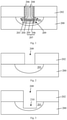
- FIG. 1 is a schematic structural diagram of a semiconductor structure according to one embodiment.
- the semiconductor structure of this embodiment includes:
- a material of the semiconductor substrate 200 may be silicon (Si), germanium (Ge), or silicon germanium (GeSi), silicon carbide (SiC). Moreover, a material of the semiconductor substrate 200 may be silicon on insulator (SOI) or germanium on insulator (GOI). Furthermore, the semiconductor substrate 200 may be made of other materials, for example, III-V compounds such as gallium arsenide.
- the semiconductor substrate 200 in this embodiment is a silicon semiconductor substrate.
- the semiconductor substrate 200 has active regions (not shown in the figure) and trench isolation structures (not shown in the figure) for isolating the active regions.
- a semiconductor device (not shown in the figure) may be formed on the active region of the semiconductor substrate 200, and the semiconductor device includes a transistor.
- the transistor includes a gate structure arranged on the surface of the semiconductor substrate 200 and the source region or drain region 201 arranged in the semiconductor substrate on two sides of the gate structure.
- the gate structure may include a gate dielectric layer arranged on the surface of the semiconductor substrate 200, a gate electrode arranged on the gate dielectric layer, and a side wall positioned on sidewall surfaces on two sides of the gate electrode and the gate dielectric layer.
- the source region or drain region 201 is doped with impurity ions.
- the metal silicide layer 203 is arranged on the sidewall of the groove 209, and the metal silicide layer 203 is shaped like a hollow ring.
- the metal silicide layer 203 can reduce a contact resistance between the conductive layer or a conducting plug and the source region or drain region 201.
- the metal silicide layer 203 has a certain junction leakage current.
- a material of the metal silicide layer 203 includes one or more of cobalt silicide, nickel silicide, platinum silicide, tantalum silicide, molybdenum silicide, and titanium silicide.
- the metal silicide layer 203 has a thickness of 10-50nm.
- the metal silicide layer 203 is formed on the sidewall of the groove 209 to reduce the contact resistance
- the insulating layer 204 is formed on the bottom of the groove 209, such that when electric current is transmitted downward from the conductive layer 208, the insulating layer 204 may form a barrier. Therefore, the electric current may be blocked by the insulating layer 204 in a vertical direction, and can only flow to a direction (the direction of arrow as shown in FIG. 1 ) toward the sidewall of the groove 209, rather than vertically leaking into the semiconductor substrate 200 at the bottom of the insulating layer 204. In this way, the impact of the electric current on the source region or drain region 201 is reduced, and the probability of occurrence of device defects is reduced.
- the source region or drain region 201 of a planar-type field effect transistor is arranged transversely. Therefore, when the electric current transversely flows from the conductive layer 208 to the source region or drain region, it is easier to implement conduction of the electric current between the source region and the drain region, and the leakage current from the source region to the semiconductor substrate 200 or the leakage current from the drain region to the semiconductor substrate 200 can be reduced, and thus the conduction performance of the field effect transistor can be effectively improved.
- a material of the insulating layer 204 is a non-conducting insulating material.
- the material of the insulating layer 204 is one or more of cobalt oxide, nickel oxide, platinum oxide, tantalum oxide, molybdenum oxide, and titanium oxide.
- the insulating layer 204 has a thickness of 1-2 nm. When the electric current is transmitted downward from the conductive layer 208, the insulating layer can better block the electric current.
- the insulating layer 204 has the same metallic elements as the metal silicide layer 203 to simplify the manufacturing process. For example, when the material of the metal silicide layer 203 is cobalt silicide, the material of the insulating layer 204 is cobalt oxide.
- the contact structure further includes a buffer layer 207, and the buffer layer 207 covers the insulating layer 204 and correspondingly covers the metal silicide layer 203 on the sidewall of the groove 209.
- the buffer layer 207 plays a role in blocking metal diffusion of the conductive layer 208, buffering a stress, and matching an adhesion force between film layers.
- the buffer layer 207 may include a titanium nitride layer and a titanium layer arranged on the titanium nitride layer, or include a tantalum nitride layer and a tantalum layer arranged on the tantalum nitride layer, or include a gallium layer and a gallium nitride layer arranged on the gallium layer.
- the buffer layer 207 includes a titanium nitride layer 205 and a titanium layer 206 arranged on the titanium nitride layer 205.
- the titanium nitride layer 205 has a thickness of 2-4 nm
- the titanium layer 206 has a thickness of 2-4 nm.
- the conductive layer 208 full fills the groove, and the material of the conductive layer 45 may be a conducting material such as copper or tungsten.
- the semiconductor substrate 200 further has a dielectric layer 202.
- the dielectric layer 202 has a through hole exposing a partial surface of the source region or drain region 201, a position of the through hole is corresponding to that of the groove 209, and the conductive layer 208 extends upward to full fill the through hole.
- the buffer layer 207 may also cover a sidewall of the through hole.
- the semiconductor substrate 200 may have a dielectric layer 202.
- the dielectric layer 202 has a through hole exposing a partial surface of the source region or drain region 201, and a conducting plug is formed in the through hole.
- the conducting plug is arranged above the conductive layer 208, and the conducting plug is electrically connected to the conductive layer.
- the dielectric layer 202 may be of a single-layered or multi-layered stack structure, and made of silicon oxide, silicon nitride, silicon oxynitride, fluorine-doped silicon dioxide (FSG), boron-doped silicon dioxide (BSG), phosphorus-doped silicon dioxide (PSG) or boron-phosphorus-doped silicon dioxide (BPSG), low-K materials, other suitable materials and/or combinations of the above materials.
- FSG fluorine-doped silicon dioxide
- BSG boron-doped silicon dioxide
- PSG phosphorus-doped silicon dioxide
- BPSG boron-phosphorus-doped silicon dioxide
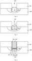
- FIG. 2-FIG. 8 are schematic structural diagrams showing a formation process of the semiconductor structure according to an embodiment of the present disclosure.
- a semiconductor substrate 200 having a source region or drain region 201 therein is provided.
- the semiconductor substrate 200 has active regions (not shown in the figure) and trench isolation structures (not shown in the figure) for isolating the active regions.
- a semiconductor device (not shown in the figure) may be formed on the active region of the semiconductor substrate 200, and the semiconductor device includes a transistor.
- the source region or drain region 201 is a source/drain region of the transistor, a gate structure (not shown in the figure) is also formed on the semiconductor substrate 200, and the source region or drain region 201 is respectively arranged in the semiconductor substrate 200 on two sides of the gate structure.
- the gate structure may include a gate dielectric layer arranged on the surface of the semiconductor substrate 200, a gate electrode arranged on the gate dielectric layer, and a side wall positioned on sidewall surfaces on two sides of the gate electrode and the gate dielectric layer.
- a material of the gate dielectric layer may be silicon oxide or a high-K dielectric material, and a material of the gate electrode may be polysilicon or a metal.
- a dielectric layer 202 may be formed on the semiconductor substrate 200, and the dielectric layer 202 has a through hole 209 exposing a partial surface of the source region or drain region 201.
- the through hole 209 is formed in the dielectric layer by using an etching process.
- the dielectric layer 202 may not be formed on the semiconductor substrate 200, and subsequently the source region or drain region 201 is directly etched to form the groove in the source region or drain region 201.
- the groove 210 is formed in the source region or drain region 201.
- an objective of forming the groove 210 is to facilitate the subsequent formation of the metal silicide layer on the sidewall of the groove 210 and the formation of the insulating layer at the bottom of the groove, and the formed metal silicide layer has a certain height. Subsequently, the insulating layer is formed at the bottom of the groove and the conductive layer is formed on the insulating layer. In this way, it is ensured that the electric current of the conductive layer can flow to the corresponding source region or drain region through the metal silicide layer without having a negative effect on the conduction between the source region and the drain region.
- the source region or drain region 201 at the bottom of the through hole 209 is etched along the through hole 209 in the dielectric layer 202, and the groove 210 is formed in the source region or drain region 201, and the source region or drain region 201 may be etched by using wet and dry etching processes.
- the formed groove 210 is wider than the source region (or drain region) 201, and the source region (or drain region) 201 is deeper than the groove 210.
- a patterned mask layer may be formed on the semiconductor substrate, wherein the patterned mask layer has an opening exposing the partial surface of the source region or drain region 201.
- the source region or drain region 201 is etched by using the patterned mask layer as a mask, and the groove is formed in the source region or drain region 201.
- the number of grooves 210 in the source region or drain region 201 may be at least one (more than or equal to two).
- the metal silicide layer 203 is formed on the surface of the sidewall of the groove 210.
- a material of the insulating layer 204 is a non-conducting insulating material.
- the material of the insulating layer 204 is one or more of cobalt oxide, nickel oxide, platinum oxide, tantalum oxide, molybdenum oxide, and titanium oxide.
- the insulating layer 204 has a thickness of 1-2 nm. When the electric current is transmitted downward from the conductive layer 208, the insulating layer can better block the electric current.
- the insulating layer 204 has the same metallic elements as the metal silicide layer 203 to simplify the manufacturing process. For example, when the material of the metal silicide layer 203 is cobalt silicide, the material of the insulating layer 204 is cobalt oxide.
- the formation process of the metal silicide layer 201 is as below.
- a metal layer (not shown in the figure) is formed on the sidewall and the bottom surface of the groove 210, the sidewall and the bottom surface of the through hole 209, and the surface of the dielectric layer 202.
- the material of the metal layer is one or more of cobalt, nickel, platinum, tantalum, molybdenum, and titanium.
- the rapid thermal annealing is performed, such that the metal in the metal layer reacts with silicon in the source region or drain region 201 to form the metal silicide layer.
- the unreacted metal layer on the sidewall of the through hole 209 and the surface of the dielectric layer 202 is removed, wherein the unreacted metal layer may be removed by wet etching.
- the metal silicide layer at the bottom of the groove 210 is removed by etching, and the metal silicide layer 203 is formed on the surface of the sidewall of the groove 210, wherein the metal silicide layer at the bottom of the groove 210 may be removed by using an anisotropic dry etching process.
- the insulating layer 204 is formed on the bottom surface of the groove 209.
- the formation process of the insulating layer 204 is as below.
- An insulating material layer is formed on the sidewall and the bottom surface of the groove 210, the sidewall surface of the through hole 209, and the surface of the dielectric layer 202.
- the insulating material layer is formed by using a deposition process.
- the insulating material layer on the sidewall surface of the groove 210, the sidewall surface of the through hole 209, and the surface of the dielectric layer 202 is removed by etching, and the insulating layer 204 is formed on the bottom surface of the groove 210, wherein an edge of the insulating layer 204 is in contact with the bottom surface of the metal silicide layer 201 on the sidewall of the groove 210.
- a material of the insulating layer 204 is a non-conducting insulating material.
- the material of the insulating layer 204 is one or more of cobalt oxide, nickel oxide, platinum oxide, tantalum oxide, molybdenum oxide, and titanium oxide.
- the insulating layer 204 has a thickness of 1-2 nm. When the electric current is transmitted downward from the conductive layer 208, the insulating layer can better block the electric current.
- the insulating layer 204 has the same metallic elements as the metal silicide layer 203 to simplify the manufacturing process. For example, when the material of the metal silicide layer 203 is cobalt silicide, the material of the insulating layer 204 is cobalt oxide.
- a conductive layer 208 is formed on the insulating layer 204, and the conductive layer 208 full fills the groove.
- the conductive layer 208 not only full fills the groove 210 (referring to FIG. 5 ), but also full fills the through hole 209 (referring to FIG. 5 ).
- the conductive layer 208 may only fill the groove 210 (referring to FIG. 5 ).
- the material of the conductive layer 208 may be Cu, Al, W or other conducting materials.
- a buffer layer 207 is formed on the insulating layer 204 before the formation of the conductive layer 208.
- the buffer layer 207 may include a titanium nitride layer and a titanium layer arranged on the titanium nitride layer, or include a tantalum nitride layer and a tantalum layer arranged on the tantalum nitride layer, or include a gallium layer and a gallium nitride layer arranged on the gallium layer.
- the buffer layer 207 includes a titanium nitride layer 205 and a titanium layer 206 arranged on the titanium nitride layer 205.
- the titanium nitride layer 205 has a thickness of 2-4 nm
- the titanium layer 206 has a thickness of 2-4 nm.
- the buffer layer 207 may also cover the sidewall surface of the through hole in addition to covering the sidewall surface of the groove.
- FIG. 7 is a schematic structural diagram showing a vertical view of the semiconductor structure as shown in FIG. 6 after the conductive layer 208 is formed in an embodiment, wherein neither the dielectric layer 202 nor the buffer layer 207 is shown in FIG. 7 .
- the source region or drain region 201 is respectively arranged in the semiconductor substrate on two sides of the gate structure 300.
- the source region or drain region 201 has a groove, and on the sidewall of the groove there is provided with the metal silicide layer 203.
- An insulating layer 204 is arranged at the bottom of the groove (referring to FIG. 6 ), the conductive layer 208 is arranged on the insulating layer 204, and the conductive layer 208 full fills the groove.
- FIG. 7 is a schematic structural diagram showing a vertical view of the semiconductor structure as shown in FIG. 6 after the conductive layer 208 is formed in an embodiment, wherein neither the dielectric layer 202 nor the buffer layer 207 is shown in FIG. 7 .
- the source region or drain region 201 is respectively arranged in the semiconductor substrate on two sides of the gate structure 300.
- the source region or drain region 201 has a groove, and on the sidewall of the groove there is provided with the metal silicide layer 203.
- An insulating layer 204 is arranged at the bottom of the groove (referring to FIG. 6 ), the conductive layer 208 is arranged on the insulating layer 204, and the conductive layer 208 full fills the groove.
- a metal layer 301 electrically connected to the conductive layer 208 may be formed on the conductive layer 208.
- FIG. 8 is a schematic structural diagram showing a vertical view of the semiconductor structure as shown in FIG. 6 after the conductive layer 208 is formed, wherein neither the dielectric layer 202 nor the buffer layer 207 is shown in FIG. 8 .
- the source region or drain region 201 is respectively arranged in the semiconductor substrate on two sides of the gate structure 300, and the source region or drain region 201 has a plurality of grooves. Reference is made by taking an example where the source region or drain region 201 has two grooves, wherein on the sidewall of each of the grooves there is provided with the metal silicide layer 203.
- An insulating layer 204 is arranged at the bottom of each of the grooves (referring to FIG.
- the conductive layer 208 is arranged on the insulating layer 204, and the conductive layer 208 full fills the grooves. Subsequently, a metal layer 302 electrically connected to a plurality of conductive layers 208 on the source region or drain region 201 may be formed on the conductive layer 208.
Landscapes
- Insulated Gate Type Field-Effect Transistor (AREA)
- Engineering & Computer Science (AREA)
- Electrodes Of Semiconductors (AREA)
- Chemical & Material Sciences (AREA)
- Materials Engineering (AREA)
- Nanotechnology (AREA)
- Manufacturing & Machinery (AREA)
Applications Claiming Priority (2)
| Application Number | Priority Date | Filing Date | Title |
|---|---|---|---|
| CN201910402381.9A CN111952367B (zh) | 2019-05-15 | 2019-05-15 | 半导体结构及其形成方法 |
| PCT/CN2019/127854 WO2020228334A1 (zh) | 2019-05-15 | 2019-12-24 | 半导体结构及其形成方法 |
Publications (2)
| Publication Number | Publication Date |
|---|---|
| EP3971992A1 true EP3971992A1 (de) | 2022-03-23 |
| EP3971992A4 EP3971992A4 (de) | 2022-06-22 |
Family
ID=73289763
Family Applications (1)
| Application Number | Title | Priority Date | Filing Date |
|---|---|---|---|
| EP19928607.1A Pending EP3971992A4 (de) | 2019-05-15 | 2019-12-24 | Halbleiterstruktur und verfahren zur formung davon |
Country Status (4)
| Country | Link |
|---|---|
| US (2) | US11302789B2 (de) |
| EP (1) | EP3971992A4 (de) |
| CN (1) | CN111952367B (de) |
| WO (1) | WO2020228334A1 (de) |
Families Citing this family (4)
| Publication number | Priority date | Publication date | Assignee | Title |
|---|---|---|---|---|
| CN111952367B (zh) * | 2019-05-15 | 2024-06-07 | 长鑫存储技术有限公司 | 半导体结构及其形成方法 |
| CN115602648A (zh) * | 2021-07-09 | 2023-01-13 | 长鑫存储技术有限公司(Cn) | 半导体结构及其制作方法 |
| CN115602612A (zh) * | 2021-07-12 | 2023-01-13 | 长鑫存储技术有限公司(Cn) | 接触插塞结构、半导体结构及其制备方法 |
| CN115621228A (zh) * | 2021-07-12 | 2023-01-17 | 长鑫存储技术有限公司 | 接触插塞结构、半导体结构及其制备方法 |
Family Cites Families (21)
| Publication number | Priority date | Publication date | Assignee | Title |
|---|---|---|---|---|
| KR100344818B1 (ko) * | 1997-09-24 | 2002-11-18 | 주식회사 하이닉스반도체 | 반도체소자및그의제조방법 |
| US20050274951A1 (en) * | 2004-06-14 | 2005-12-15 | Howard Gregory E | MOSFET having channel in bulk semiconductor and source/drain on insulator, and method of fabrication |
| US20050280085A1 (en) * | 2004-06-16 | 2005-12-22 | Cree Microwave, Inc. | LDMOS transistor having gate shield and trench source capacitor |
| JP2006228859A (ja) * | 2005-02-16 | 2006-08-31 | Matsushita Electric Ind Co Ltd | 半導体装置およびその製造方法 |
| US7932556B2 (en) * | 2007-12-14 | 2011-04-26 | Fairchild Semiconductor Corporation | Structure and method for forming power devices with high aspect ratio contact openings |
| CN101640218B (zh) * | 2009-06-09 | 2012-08-08 | 上海宏力半导体制造有限公司 | 金属氧化物半导体场效应晶体管及其制造方法 |
| JP2011222769A (ja) * | 2010-04-09 | 2011-11-04 | Renesas Electronics Corp | 半導体装置 |
| KR101873911B1 (ko) * | 2011-06-07 | 2018-07-04 | 삼성전자주식회사 | 콘택 구조체를 포함하는 반도체 소자와 그 제조방법, 및 그것을 포함하는 전자 시스템 |
| CN103000675B (zh) * | 2011-09-08 | 2015-11-25 | 中国科学院微电子研究所 | 低源漏接触电阻mosfets及其制造方法 |
| CN103426768B (zh) * | 2012-05-25 | 2016-08-10 | 中国科学院微电子研究所 | 半导体器件制造方法 |
| US9231098B2 (en) * | 2013-10-30 | 2016-01-05 | Taiwan Semiconductor Manufacturing Co., Ltd. | Mechanism for forming metal gate structure |
| US9673295B2 (en) * | 2014-05-27 | 2017-06-06 | Globalfoundries Inc. | Contact resistance optimization via EPI growth engineering |
| US9799687B2 (en) * | 2014-06-19 | 2017-10-24 | Joled Inc. | Method for manufacturing active-matrix display panel, and active-matrix display panel |
| US9773681B2 (en) * | 2015-06-05 | 2017-09-26 | Vanguard International Semiconductor Corporation | Semiconductor device with a trench and method for manufacturing the same |
| US9484255B1 (en) * | 2015-11-03 | 2016-11-01 | International Business Machines Corporation | Hybrid source and drain contact formation using metal liner and metal insulator semiconductor contacts |
| KR102600998B1 (ko) * | 2016-09-28 | 2023-11-13 | 삼성전자주식회사 | 반도체 장치 |
| CN108573910B (zh) * | 2017-03-07 | 2020-10-09 | 中芯国际集成电路制造(上海)有限公司 | 半导体结构及其形成方法 |
| CN209045566U (zh) * | 2018-11-30 | 2019-06-28 | 长鑫存储技术有限公司 | 导电插塞结构及半导体器件 |
| TWI696285B (zh) * | 2019-05-02 | 2020-06-11 | 力晶積成電子製造股份有限公司 | 記憶體結構 |
| CN210092094U (zh) * | 2019-05-15 | 2020-02-18 | 长鑫存储技术有限公司 | 半导体结构 |
| CN111952367B (zh) * | 2019-05-15 | 2024-06-07 | 长鑫存储技术有限公司 | 半导体结构及其形成方法 |
-
2019
- 2019-05-15 CN CN201910402381.9A patent/CN111952367B/zh active Active
- 2019-12-24 WO PCT/CN2019/127854 patent/WO2020228334A1/zh not_active Ceased
- 2019-12-24 EP EP19928607.1A patent/EP3971992A4/de active Pending
-
2020
- 2020-11-02 US US17/087,431 patent/US11302789B2/en active Active
-
2022
- 2022-04-10 US US17/717,115 patent/US20220238665A1/en not_active Abandoned
Also Published As
| Publication number | Publication date |
|---|---|
| WO2020228334A1 (zh) | 2020-11-19 |
| US20210050424A1 (en) | 2021-02-18 |
| CN111952367B (zh) | 2024-06-07 |
| US20220238665A1 (en) | 2022-07-28 |
| US11302789B2 (en) | 2022-04-12 |
| CN111952367A (zh) | 2020-11-17 |
| EP3971992A4 (de) | 2022-06-22 |
Similar Documents
| Publication | Publication Date | Title |
|---|---|---|
| US11575044B2 (en) | Integrated circuit device | |
| US20220238665A1 (en) | Semiconductor structure and formation method thereof | |
| US8835316B2 (en) | Transistor with primary and semiconductor spacer, method for manufacturing transistor, and semiconductor chip comprising the transistor | |
| TWI759277B (zh) | 半導體元件、鰭式場效電晶體元件及其形成方法 | |
| EP3968376A1 (de) | Halbleiterbauelemente | |
| US11621332B2 (en) | Wraparound contact to a buried power rail | |
| CN114334827B (zh) | 半导体结构及其形成方法 | |
| US20110298017A1 (en) | Replacement gate mosfet with self-aligned diffusion contact | |
| US10283617B1 (en) | Hybrid spacer integration for field-effect transistors | |
| US10832983B2 (en) | Semiconductor device having a trench type device isolation film and method for fabricating the same | |
| TWI697985B (zh) | 半導體裝置及其製造方法 | |
| KR20190081071A (ko) | 반도체 소자 | |
| TW202205596A (zh) | 半導體裝置 | |
| TW202119479A (zh) | 半導體裝置結構及其形成方法 | |
| CN104183543B (zh) | 电熔丝结构及其形成方法、半导体器件 | |
| WO2023236264A1 (zh) | 一种半导体结构及其制造方法 | |
| US12382681B2 (en) | Multi-bridge channel field effect transistor with reduced gate-channel leakage current | |
| US20230411469A1 (en) | Semiconductor structure and formation method thereof | |
| US6667204B2 (en) | Semiconductor device and method of forming the same | |
| WO2022061737A1 (zh) | 半导体结构及其形成方法 | |
| CN210092094U (zh) | 半导体结构 | |
| US20240021728A1 (en) | Semiconductor structure and fabrication method thereof | |
| US11869952B2 (en) | Semiconductor structure and method for forming same | |
| US10008385B1 (en) | Enlarged sacrificial gate caps for forming self-aligned contacts | |
| US9570449B2 (en) | Metal strap for DRAM/FinFET combination |
Legal Events
| Date | Code | Title | Description |
|---|---|---|---|
| STAA | Information on the status of an ep patent application or granted ep patent |
Free format text: STATUS: THE INTERNATIONAL PUBLICATION HAS BEEN MADE |
|
| PUAI | Public reference made under article 153(3) epc to a published international application that has entered the european phase |
Free format text: ORIGINAL CODE: 0009012 |
|
| STAA | Information on the status of an ep patent application or granted ep patent |
Free format text: STATUS: REQUEST FOR EXAMINATION WAS MADE |
|
| 17P | Request for examination filed |
Effective date: 20210708 |
|
| AK | Designated contracting states |
Kind code of ref document: A1 Designated state(s): AL AT BE BG CH CY CZ DE DK EE ES FI FR GB GR HR HU IE IS IT LI LT LU LV MC MK MT NL NO PL PT RO RS SE SI SK SM TR |
|
| A4 | Supplementary search report drawn up and despatched |
Effective date: 20220519 |
|
| RIC1 | Information provided on ipc code assigned before grant |
Ipc: H01L 29/06 20060101ALI20220513BHEP Ipc: H01L 29/417 20060101ALI20220513BHEP Ipc: H01L 29/45 20060101ALI20220513BHEP Ipc: H01L 29/78 20060101AFI20220513BHEP |
|
| DAV | Request for validation of the european patent (deleted) | ||
| DAX | Request for extension of the european patent (deleted) | ||
| STAA | Information on the status of an ep patent application or granted ep patent |
Free format text: STATUS: EXAMINATION IS IN PROGRESS |
|
| 17Q | First examination report despatched |
Effective date: 20231121 |
|
| REG | Reference to a national code |
Ref country code: DE Ref legal event code: R079 Free format text: PREVIOUS MAIN CLASS: H01L0029780000 Ipc: H10D0030010000 |
|
| GRAP | Despatch of communication of intention to grant a patent |
Free format text: ORIGINAL CODE: EPIDOSNIGR1 |
|
| STAA | Information on the status of an ep patent application or granted ep patent |
Free format text: STATUS: GRANT OF PATENT IS INTENDED |
|
| RIC1 | Information provided on ipc code assigned before grant |
Ipc: H10D 30/01 20250101AFI20260202BHEP Ipc: H10D 30/60 20250101ALI20260202BHEP Ipc: H10D 62/00 20260101ALI20260202BHEP Ipc: H10D 62/10 20250101ALI20260202BHEP Ipc: H10D 62/13 20250101ALI20260202BHEP Ipc: H10D 64/01 20250101ALI20260202BHEP Ipc: H10D 64/23 20250101ALI20260202BHEP Ipc: H10D 64/62 20250101ALI20260202BHEP Ipc: H10D 62/832 20250101ALI20260202BHEP |
|
| INTG | Intention to grant announced |
Effective date: 20260212 |
|
| P01 | Opt-out of the competence of the unified patent court (upc) registered |
Free format text: CASE NUMBER: UPC_APP_0009309_3971992/2026 Effective date: 20260311 |
|
| GRAS | Grant fee paid |
Free format text: ORIGINAL CODE: EPIDOSNIGR3 |
|
| GRAA | (expected) grant |
Free format text: ORIGINAL CODE: 0009210 |
|
| STAA | Information on the status of an ep patent application or granted ep patent |
Free format text: STATUS: THE PATENT HAS BEEN GRANTED |