EP3972156A1 - Amplificateurs optiques intégrés à semi-conducteurs pour la photonique au silicium - Google Patents
Amplificateurs optiques intégrés à semi-conducteurs pour la photonique au silicium Download PDFInfo
- Publication number
- EP3972156A1 EP3972156A1 EP21190283.8A EP21190283A EP3972156A1 EP 3972156 A1 EP3972156 A1 EP 3972156A1 EP 21190283 A EP21190283 A EP 21190283A EP 3972156 A1 EP3972156 A1 EP 3972156A1
- Authority
- EP
- European Patent Office
- Prior art keywords
- soa
- path
- polarization
- modulator
- splitter
- Prior art date
- Legal status (The legal status is an assumption and is not a legal conclusion. Google has not performed a legal analysis and makes no representation as to the accuracy of the status listed.)
- Pending
Links
Images





Classifications
-
- H—ELECTRICITY
- H01—ELECTRIC ELEMENTS
- H01S—DEVICES USING THE PROCESS OF LIGHT AMPLIFICATION BY STIMULATED EMISSION OF RADIATION [LASER] TO AMPLIFY OR GENERATE LIGHT; DEVICES USING STIMULATED EMISSION OF ELECTROMAGNETIC RADIATION IN WAVE RANGES OTHER THAN OPTICAL
- H01S5/00—Semiconductor lasers
- H01S5/50—Amplifier structures not provided for in groups H01S5/02 - H01S5/30
- H01S5/5036—Amplifier structures not provided for in groups H01S5/02 - H01S5/30 the arrangement being polarisation-selective
-
- H—ELECTRICITY
- H01—ELECTRIC ELEMENTS
- H01S—DEVICES USING THE PROCESS OF LIGHT AMPLIFICATION BY STIMULATED EMISSION OF RADIATION [LASER] TO AMPLIFY OR GENERATE LIGHT; DEVICES USING STIMULATED EMISSION OF ELECTROMAGNETIC RADIATION IN WAVE RANGES OTHER THAN OPTICAL
- H01S5/00—Semiconductor lasers
- H01S5/50—Amplifier structures not provided for in groups H01S5/02 - H01S5/30
-
- H—ELECTRICITY
- H04—ELECTRIC COMMUNICATION TECHNIQUE
- H04B—TRANSMISSION
- H04B10/00—Transmission systems employing electromagnetic waves other than radio-waves, e.g. infrared, visible or ultraviolet light, or employing corpuscular radiation, e.g. quantum communication
- H04B10/50—Transmitters
- H04B10/516—Details of coding or modulation
-
- G—PHYSICS
- G02—OPTICS
- G02B—OPTICAL ELEMENTS, SYSTEMS OR APPARATUS
- G02B27/00—Optical systems or apparatus not provided for by any of the groups G02B1/00 - G02B26/00, G02B30/00
- G02B27/28—Optical systems or apparatus not provided for by any of the groups G02B1/00 - G02B26/00, G02B30/00 for polarising
- G02B27/283—Optical systems or apparatus not provided for by any of the groups G02B1/00 - G02B26/00, G02B30/00 for polarising used for beam splitting or combining
-
- G—PHYSICS
- G02—OPTICS
- G02B—OPTICAL ELEMENTS, SYSTEMS OR APPARATUS
- G02B27/00—Optical systems or apparatus not provided for by any of the groups G02B1/00 - G02B26/00, G02B30/00
- G02B27/28—Optical systems or apparatus not provided for by any of the groups G02B1/00 - G02B26/00, G02B30/00 for polarising
- G02B27/286—Optical systems or apparatus not provided for by any of the groups G02B1/00 - G02B26/00, G02B30/00 for polarising for controlling or changing the state of polarisation, e.g. transforming one polarisation state into another
-
- G—PHYSICS
- G02—OPTICS
- G02B—OPTICAL ELEMENTS, SYSTEMS OR APPARATUS
- G02B6/00—Light guides; Structural details of arrangements comprising light guides and other optical elements, e.g. couplings
- G02B6/10—Light guides; Structural details of arrangements comprising light guides and other optical elements, e.g. couplings of the optical waveguide type
- G02B6/12—Light guides; Structural details of arrangements comprising light guides and other optical elements, e.g. couplings of the optical waveguide type of the integrated circuit kind
- G02B6/12004—Combinations of two or more optical elements
-
- H—ELECTRICITY
- H01—ELECTRIC ELEMENTS
- H01S—DEVICES USING THE PROCESS OF LIGHT AMPLIFICATION BY STIMULATED EMISSION OF RADIATION [LASER] TO AMPLIFY OR GENERATE LIGHT; DEVICES USING STIMULATED EMISSION OF ELECTROMAGNETIC RADIATION IN WAVE RANGES OTHER THAN OPTICAL
- H01S5/00—Semiconductor lasers
- H01S5/005—Optical components external to the laser cavity, specially adapted therefor, e.g. for homogenisation or merging of the beams or for manipulating laser pulses, e.g. pulse shaping
-
- H—ELECTRICITY
- H01—ELECTRIC ELEMENTS
- H01S—DEVICES USING THE PROCESS OF LIGHT AMPLIFICATION BY STIMULATED EMISSION OF RADIATION [LASER] TO AMPLIFY OR GENERATE LIGHT; DEVICES USING STIMULATED EMISSION OF ELECTROMAGNETIC RADIATION IN WAVE RANGES OTHER THAN OPTICAL
- H01S5/00—Semiconductor lasers
- H01S5/02—Structural details or components not essential to laser action
- H01S5/026—Monolithically integrated components, e.g. waveguides, monitoring photo-detectors, drivers
-
- H—ELECTRICITY
- H01—ELECTRIC ELEMENTS
- H01S—DEVICES USING THE PROCESS OF LIGHT AMPLIFICATION BY STIMULATED EMISSION OF RADIATION [LASER] TO AMPLIFY OR GENERATE LIGHT; DEVICES USING STIMULATED EMISSION OF ELECTROMAGNETIC RADIATION IN WAVE RANGES OTHER THAN OPTICAL
- H01S5/00—Semiconductor lasers
- H01S5/30—Structure or shape of the active region; Materials used for the active region
- H01S5/3013—AIIIBV compounds
-
- H—ELECTRICITY
- H04—ELECTRIC COMMUNICATION TECHNIQUE
- H04B—TRANSMISSION
- H04B10/00—Transmission systems employing electromagnetic waves other than radio-waves, e.g. infrared, visible or ultraviolet light, or employing corpuscular radiation, e.g. quantum communication
- H04B10/40—Transceivers
-
- H—ELECTRICITY
- H04—ELECTRIC COMMUNICATION TECHNIQUE
- H04B—TRANSMISSION
- H04B10/00—Transmission systems employing electromagnetic waves other than radio-waves, e.g. infrared, visible or ultraviolet light, or employing corpuscular radiation, e.g. quantum communication
- H04B10/50—Transmitters
- H04B10/501—Structural aspects
- H04B10/503—Laser transmitters
- H04B10/505—Laser transmitters using external modulation
- H04B10/5053—Laser transmitters using external modulation using a parallel, i.e. shunt, combination of modulators
-
- H—ELECTRICITY
- H04—ELECTRIC COMMUNICATION TECHNIQUE
- H04B—TRANSMISSION
- H04B10/00—Transmission systems employing electromagnetic waves other than radio-waves, e.g. infrared, visible or ultraviolet light, or employing corpuscular radiation, e.g. quantum communication
- H04B10/60—Receivers
-
- H—ELECTRICITY
- H04—ELECTRIC COMMUNICATION TECHNIQUE
- H04B—TRANSMISSION
- H04B10/00—Transmission systems employing electromagnetic waves other than radio-waves, e.g. infrared, visible or ultraviolet light, or employing corpuscular radiation, e.g. quantum communication
- H04B10/60—Receivers
- H04B10/61—Coherent receivers
-
- G—PHYSICS
- G02—OPTICS
- G02B—OPTICAL ELEMENTS, SYSTEMS OR APPARATUS
- G02B6/00—Light guides; Structural details of arrangements comprising light guides and other optical elements, e.g. couplings
- G02B6/10—Light guides; Structural details of arrangements comprising light guides and other optical elements, e.g. couplings of the optical waveguide type
- G02B6/12—Light guides; Structural details of arrangements comprising light guides and other optical elements, e.g. couplings of the optical waveguide type of the integrated circuit kind
- G02B2006/12083—Constructional arrangements
- G02B2006/12123—Diode
-
- G—PHYSICS
- G02—OPTICS
- G02B—OPTICAL ELEMENTS, SYSTEMS OR APPARATUS
- G02B6/00—Light guides; Structural details of arrangements comprising light guides and other optical elements, e.g. couplings
- G02B6/10—Light guides; Structural details of arrangements comprising light guides and other optical elements, e.g. couplings of the optical waveguide type
- G02B6/12—Light guides; Structural details of arrangements comprising light guides and other optical elements, e.g. couplings of the optical waveguide type of the integrated circuit kind
- G02B2006/12133—Functions
- G02B2006/12159—Interferometer
-
- G—PHYSICS
- G02—OPTICS
- G02B—OPTICAL ELEMENTS, SYSTEMS OR APPARATUS
- G02B6/00—Light guides; Structural details of arrangements comprising light guides and other optical elements, e.g. couplings
- G02B6/24—Coupling light guides
- G02B6/26—Optical coupling means
- G02B6/27—Optical coupling means with polarisation selective and adjusting means
- G02B6/2753—Optical coupling means with polarisation selective and adjusting means characterised by their function or use, i.e. of the complete device
- G02B6/2773—Polarisation splitting or combining
-
- G—PHYSICS
- G02—OPTICS
- G02B—OPTICAL ELEMENTS, SYSTEMS OR APPARATUS
- G02B6/00—Light guides; Structural details of arrangements comprising light guides and other optical elements, e.g. couplings
- G02B6/24—Coupling light guides
- G02B6/42—Coupling light guides with opto-electronic elements
- G02B6/4201—Packages, e.g. shape, construction, internal or external details
- G02B6/4204—Packages, e.g. shape, construction, internal or external details the coupling comprising intermediate optical elements, e.g. lenses, holograms
- G02B6/4213—Packages, e.g. shape, construction, internal or external details the coupling comprising intermediate optical elements, e.g. lenses, holograms the intermediate optical elements being polarisation selective optical elements
-
- H—ELECTRICITY
- H01—ELECTRIC ELEMENTS
- H01S—DEVICES USING THE PROCESS OF LIGHT AMPLIFICATION BY STIMULATED EMISSION OF RADIATION [LASER] TO AMPLIFY OR GENERATE LIGHT; DEVICES USING STIMULATED EMISSION OF ELECTROMAGNETIC RADIATION IN WAVE RANGES OTHER THAN OPTICAL
- H01S5/00—Semiconductor lasers
- H01S5/06—Arrangements for controlling the laser output parameters, e.g. by operating on the active medium
- H01S5/068—Stabilisation of laser output parameters
- H01S5/0683—Stabilisation of laser output parameters by monitoring the optical output parameters
-
- H—ELECTRICITY
- H01—ELECTRIC ELEMENTS
- H01S—DEVICES USING THE PROCESS OF LIGHT AMPLIFICATION BY STIMULATED EMISSION OF RADIATION [LASER] TO AMPLIFY OR GENERATE LIGHT; DEVICES USING STIMULATED EMISSION OF ELECTROMAGNETIC RADIATION IN WAVE RANGES OTHER THAN OPTICAL
- H01S5/00—Semiconductor lasers
- H01S5/40—Arrangement of two or more semiconductor lasers, not provided for in groups H01S5/02 - H01S5/30
- H01S5/4025—Array arrangements, e.g. constituted by discrete laser diodes or laser bar
Definitions
- Embodiments of the present disclosure generally relate to the field of photonic integrated circuits (PIC), in particular semiconductor optical amplifiers (SOA) integrated into silicon photonic devices.
- PIC photonic integrated circuits
- SOA semiconductor optical amplifiers
- Computing platforms are increasingly using photonic integrated circuits for coherent optical links to increase transmission capacity by modulating both amplitude and phase of an optical signal.
- Embodiments described herein may be directed to a silicon photonics integrated apparatus that includes an input to receive an optical signal, a splitter optically coupled to the input to split the optical signal at a first path and a second path, a polarization beam splitter and rotator (PBSR) optically coupled with the first path or the second path, and a semiconductor optical amplifier (SOA) optically coupled with the first path or the second path and disposed between the splitter and the PBSR.
- PBSR polarization beam splitter and rotator
- SOA semiconductor optical amplifier
- Silicon photonics high speed coherent in-phase quadrature (IQ) modulator and the associated receivers can support 600Gb/s transmission based on a 64GBaud and 64 quadrature amplitude modulation (QAM) high order modulation scheme. They can also support higher baud rate and higher QAM modulation combinations for higher rates of transmission beyond 600Gb/s, such as 800Gb/s or 1.2Tb/s, based on optimization of silicon photonics modulator physical layer designs.
- QAM quadrature amplitude modulation
- coherent IQ modulators require a number of elements, such as an optical splitter to split the signal into two different branches designated for two different polarizations, phase shifters, polarization rotator, polarization combiner, and many optical coupler taps at different locations in order to monitor the input or output optical power at different locations within the IQ modulator. These elements will cause significant power loss to the incoming optical power from the tunable laser. Second, and more important, the higher the order of the QAM modulation, the higher the effective optical loss.
- the extra modulation induced optical signal loss is about 10dB.
- the combination of the physical transmission induced loss and the modulation induced loss, and with the assumption that the increase of optical output power from the tunable laser is hard to achieve, for example, greater than 20dBm it is difficult to have enough output optical power from the coherent IQ modulator operating at high order QAM modulation.
- the resulting output power may be low when high yield is needed.
- the output power is usually around - 8dBm to -12dBm.
- the requirement may be -6dBm to +4dBm.
- the gap is anywhere from 2dB to 16dB depending on the applications for 400Gb/s case.
- 600Gb/s, 800Gb/s or higher rate of operation with higher order QAM modulation the modulation induced loss is much higher, and the output signal needs to be higher accordingly. So there is a challenge of a bottleneck of an ever larger gap in required optical power.
- optical amplification element is added or co-packaged to the output of the tunable laser to boost the output power of the laser before it gets coupled into the modulator.
- an optical amplification element may be co-packaged onto the output port of the silicon photonics modulator.
- optical amplification elements can be co-packaged into the two receiver arms in order to increase the receiver sensitivity and increase the reach of the transmission from the transceiver to the receiver.
- the coupling from outside elements into or from the silicon photonics modulator and receiver is challenging due to the added coupling loss, the need for complex coupling lenses, the increase in the package size, the need for optical isolators, and a significant amount of complex optical alignment work and associated cost.
- the resulting packages may be too big, too costly, and unfit for pluggable module applications.
- legacy implementations use silicon photonics based coherent IQ modulators and receivers without integrated SOAs.
- power is not sufficient for 400Gb/s or 800Gb/s data center interconnect applications, nor for the metro applications where distances may be beyond 80km.
- Embodiments described herein may be directed to hybrid integration technology of Indium Phosphide (InP) or other materials onto a silicon photonics platform. This technology increases the quality and reliability, compared to legacy implementations described above, and may be produced with a lower cost and higher volume. In addition, these embodiments may support complex integration of many different functions implemented on a photonics platform. Embodiments may include integrating hybrid InP-based SOAs into various arms of a silicon photonics based modulator and/or receiver.
- InP Indium Phosphide
- Embodiments may be directed to a new transmitter architecture design where a silicon photonics modulator and receiver will be integrated with InP-based SOAs. In embodiments, they will be integrated using wafer bonding technology. Embodiments of these hybrid SOA integrated modulators and receiver combine the best of two material systems: InP for amplification and silicon photonics material for the modulator and receiver. Embodiments may enable high speed modulation to support high capacity coherent applications at 400Gb/s, 800Gb/s to 1 Tb/s per wavelength and beyond.
- III-V/Si hybrid SOA in silicon photonics platforms may enable energy efficient, reduced complexity, and lower cost photonics systems.
- embodiments are disclosed that use optimized implementations of III-V/Si hybrid SOA at key locations within a photonics system to support higher data rates.
- Silicon photonic optical transceivers offer an energy efficient high bandwidth density solution needed to overcome the I/O constraints in scaling high performance computing.
- Hybrid silicon optical amplifiers can be integrated in either the transmitter or receiver to amplify the optical signal and compensate for losses in the optical link as an alternative to a higher power laser source. Placing an SOA within a transmitter may limit the benefit of an SOA if the amplified back reflection to an integrated laser leads to elevated noise that will degrade the optical signal.
- Embodiments may also be directed to an optical isolator placed after the laser or after the transmitter where one or more SOAs can be integrated in a silicon photonic receiver with germanium (Ge) photodetectors for optical amplification independent of negative effects to the laser.
- SOAs can be integrated in a silicon photonic receiver with germanium (Ge) photodetectors for optical amplification independent of negative effects to the laser.
- Ge germanium
- These embodiments may offer a low cost, scalable solution for input/output (I/O) in high performance computing.
- the integrated hybrid silicon SOA in the receiver amplifies the optical signal without constraints on the amplified back reflection destabilizing the laser that is integrated on the transmitter.
- Silicon photonic optical transceivers also offer a low-cost, high-volume solution needed to implement coherent optical links with 400Gb/s, 800Gb/s, and higher data transmission rates with a pluggable form factor.
- Coherent optical links increase transmission capacity by modulating both the amplitude and phase of the optical signal.
- Higher-order modulation formats such as 16 QAM and 64 QAM encode 4- and 6-bits per symbol compared to 1-bit per symbol for on-off keying, for example. This may be combined with polarization division multiplexing (PDM) to double the data in the fiber by transmitting the coherent signal in two orthogonal polarizations.
- PDM polarization division multiplexing
- a coherent dual-polarization transmitter may include a laser with IQ modulators, one for each polarization, and polarization rotator and combiner.
- the coherent optical receiver consists of a polarization beam splitter and rotator to separate the polarizations, then uses a local oscillator (a reference optical signal) mixed with the incoming SATA signal in a 90-degree optical hybrid with balanced photodetectors to convert the phase and amplitude modulated signal optical signal into the electrical domain.
- a coherent transceiver light from the same laser source can be split and used for both transmission and for the receiver local oscillator.
- legacy implementations due to the losses of the components in the link, particularly from the IQ modulators themselves and the effective loss due to the modulation format, it is challenging to meet the link budget without amplification. In legacy implementations there may be a gap in power of 6-16dB depending on the application and the modulation format.
- SOAs semiconductor optical amplifiers
- integrating them within the silicon photonic transceiver may provide a low-cost and compact solution to boost the signal in order to close the link.
- phrase “A and/or B” means (A), (B), or (A and B).
- phrase “A, B, and/or C” means (A), (B), (C), (A and B), (A and C), (B and C), or (A, B, and C).
- Coupled may mean one or more of the following. “Coupled” may mean that two or more elements are in direct physical or electrical contact. However, “coupled” may also mean that two or more elements indirectly contact each other, but yet still cooperate or interact with each other, and may mean that one or more other elements are coupled or connected between the elements that are said to be coupled with each other.
- directly coupled may mean that two or more elements are in direct contact.
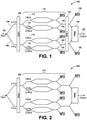
- FIGs. 1-4 illustrate coherent transmitters and receivers that include hybrid integrated SOAs for amplification.
- These embodiments may include elements and structure of a Mach-Zehnder (MZ) modulator that is used for controlling the characteristics of an optical wave.
- MZ Mach-Zehnder
- an input waveguide is split up into two waveguide interferometer arms. If a voltage is applied across one of the arms, a phase shift is induced for the wave passing through that arm. When the two arms are recombined, the phase difference between the two waves is converted to an amplitude modulation.
- MZ Mach-Zehnder
- configurations of the silicon photonic hybrid SOA integrated modulator and receiver are in the shape of a MZ modulator and coherent receiver, wherein the SOA structure is defined in various locations in the MZ arms as shown in FIGs. 1-3 and in the receiver arms as shown in FIG. 4 .
- the SOAs may be defined by the silicon waveguides on the device wafer, which are in alignment with the underneath input and output waveguides of the MZ arms and receiver arms.
- the laser light coming into the SOA input port is gradually coupled vertically upwards to the SOA epitaxial (EPI) materials and waveguide structure as defined by the implantation to the InP EPI materials.
- the output light from SOA is then gradually coupled downwards to the MZ's input waveguide.
- the modulator output light coming into the SOA input port is gradually coupled vertically upwards to the SOA EPI materials and waveguide structure as defined by the implantation to the InP EPI materials.
- the output light from SOA is then gradually coupled downwards to the MZ's output waveguide.
- FIG. 1 illustrates a coherent transmitter that includes hybrid integrated SOAs for pre-amplification before a modulator and post amplification after the modulator, in accordance with various embodiments.
- Transmitter 100 shows an input 102, which may be a waveguide input, that is split into an X polarization 104 and a Y polarization 106.
- the light is subsequently amplified using an InP SOA 108.
- the light may subsequently go through other splitting and coupling through an MZ structure 110 that may include in-phase modulators 112, quadrature modulator 114, and monitor photodiodes (MPD) 116.
- MPD monitor photodiodes
- the outputs 118, 120 of the MZ structure 100 then go through another InP SOA 122 for signal amplification prior to being combined by a Polarization Rotator Beam Combiner (PRBC) 124 and then outputted through output 126.
- PRBC Polarization Rotator Beam Combiner
- the SOA 122 may also couple with MPDs 128, 130.
- transmitter 100 may be referred to as a coherent transmitter with a hybrid integrated SOA for each branch after the power splitter, where SOA 108 is used for pre-amplification before the MZ structure 110, and the SOA 122 is used for post amplification after the modulator.
- FIG. 2 illustrates a coherent transmitter that includes a hybrid integrated SOA for pre-amplification before a modulator, in accordance with various embodiments.
- Transmitter 200 may be similar to transmitter 100 of FIG. 1 ; however, with transmitter 200 there is only a single SOA 208, which may be an InP SOA, prior to the MZ structure 210.
- transmitter 200 may be referred to as a coherent transmitter with hybrid integrated SOA for each branch after the power splitter, where SOA 208 is used for pre-amplification before the MZ structure 210.
- FIG. 3 illustrates a coherent transmitter that includes a hybrid integrated SOA for post amplification after a modulator, in accordance with various embodiments.
- Transmitter 300 may be similar to transmitter 100 of FIG. 1 ; however, with transmitter 300 there is only a single SOA 322, which may be an InP SOA, after the MZ structure 310.
- transmitter 300 may be referred to as a coherent transmitter with hybrid integrated SOA for each branch after the power splitter, where SOA 322 is used for post amplification after the MZ structure 310.
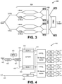
- FIG. 4 illustrates a coherent receiver that includes a hybrid integrated SOA for each of the X and Y polarization branches for pre-amplification before a detector, in accordance with various embodiments.
- Coherent receiver 400 includes an input 402 to receive light that is then passed through a variable optical attenuator (VOA) 403 and in contact with a monitoring photodetector (MPD) 405, and a PBSR 401.
- VOA variable optical attenuator
- MPD monitoring photodetector
- PBSR 401 PBSR 401.
- multiple hybrid SOAs for example, an X polarization SOA 408, and a Y polarization SOA 409 that may be placed, respectively, in two different arms 404, 406 in order to amplify the received signals in both x polarization and y polarization.
- LO local oscillator
- the output of the LO 422 goes to a beam splitter 424, which combines with the output of SOA 408 and output of SOA 409 to feed the rest of the circuit of the coherent receiver 400.
- the X and Y polarization are referring to the input signal only.
- the original X and Y polarization signals may have been converted into one orientation of physical optical polarization in the silicon photonics waveguides, normally called transverse electric (TE) mode; therefore, there are actually operated in the same polarization before they reach the SOAs 408, 409, and then subsequently amplified by SOAs 408, 409 in the same way.
- the SOAs 408, 409 may be in an InP EPI gain medium 411.
- SOAs may be placed in other locations, both outside and inside the MZ structure 110, 210, 310.
- SOAs 408, 409 may be placed in various locations for amplification within the coherent receiver 400.
- FIGs. 5-7 disclose techniques and embodiments of incorporating III-V/Si hybrid SOAs to enable energy-efficient and low cost implementations of various photonic elements including lasers ( FIG. 5 ), micro ring modulators ( FIG. 6 ), and photodiodes ( FIG. 7 ).
- FIG. 5 illustrates an energy-efficient laser that incorporates a hybrid integrated SOA, in accordance with various embodiments.
- Laser device 500 includes a laser 502 with a first end 502a that is optically coupled with a back absorber 504.
- the laser 502 has a second end 502b that is an output end optically coupled with a first end 506a of an SOA 506 to amplify a signal generated by the laser 502.
- the amplified signal is then sent through the output end 506b of the SOA 506 to the device output 508.
- the SOA 506 would be omitted.
- laser output power is an important metric for any laser
- efficiency of the laser is also an important metric for energy-efficient systems.
- Using a laser alone, such as laser 502 may be a challenge to meet both laser efficiency and output power requirements at the same time during operation.
- the laser 502 may be a III-V/Si hybrid laser
- the SOA 506 may be a III-V/Si hybrid SOA used to amplify the output of the laser 502.
- SOA 506 may be used to provide the gain needed for a given target laser output specification.
- the SOA 506 may also provide an independent way to control the output optical power, which would otherwise be difficult in legacy implementations for a laser 502 to provide on its own. For example, this independent control may provide the opportunity to split the laser 502 into multiple parallel channels to increase data rates.
- these embodiments may also allow for greater flexibility in laser 502 design for a higher back reflection tolerance and operational stability.
- a legacy, energy inefficient solution is to bias the laser at 140 mA to reach the desired power.
- the laser 502 may be biased at 55 mA, which may be the most efficient operating condition for the laser 502. Driving the laser higher than 55 mA results in higher output power, but the efficiency of the laser may substantially drop.
- the total electrical consumption from the laser 502 and the SOA 506 combination is 141 mW, with the laser 502 consuming 85 mW, giving ⁇ 8 dBm power, and the SOA consuming 56 mW, giving 4 dB gain-compared to just the laser 502, which consumes 340 mW.
- this change may result in a 240% more efficient system.
- embodiments described herein directed to integrating an SOA may be valid for any photonic apparatus or system.
- FIG. 6 illustrates a transmitter that incorporates a hybrid integrated SOA with an MRM, in accordance with various embodiments.
- Communication link 600 includes an MRM 602 that optically interacts with laser light from an input 604, and outputs light to an SOA 606. After leaving the SOA 606, the light travels to the output 608.
- Legacy implementations may use an MZ modulator, but increased requirements for data rates and power efficiency make MRMs 602 a better choice.
- MRMs 602 are a few orders of magnitude smaller than MZ modulators, thus using MRMs 602 help deliver more channels per MRM in a given footprint (not shown).
- MRMs 602 are more power efficient, especially with respect to drive electronics.
- MRMs 602 are subject to self-heating, which is primarily caused by the amount of light circulating inside the MRM 602.
- this amount of light received by an MRM 602 may be reduced without risking a closure of the communication link.
- MRM self-heating problems may be removed and enable the communication link to be closed.
- signal quality remains within measurement error ranges when using an SOA 606 after the MRM 602 in the communication link 600.
- FIG. 7 illustrates a receiver that incorporates a hybrid integrated SOA with a Si PD, in accordance with various embodiments.
- Legacy PD 700a shows an input optical signal 702 going into a Ge PD 703.
- Ge PD 703 may provide a higher response activity
- using Ge PD 703 involves a costly and complicated integration process, particularly when compared to implementing Si PDs as described below.
- Photodetector 700b shows an embodiment where an input optical signal 702 goes into an SOA 706, with an output of the SOA 706 optically coupled to a Si PD 704.
- Embodiments may include replacing the Ge PD with III-V/Si SOA in addition to a Si PD 704.
- Si PDs can be fabricated through a much simpler process than a Ge PD, resulting in low cost of implementation. Although some Si PDs may have lower responsivity compared to a Ge PD, positioning the SOA 706 in front of the Si PD 704 will amplify the signal before it is detected by the Si PD 704.
- FIGs. 8-11 include a description of embodiments of directed architectures that integrate SOAs and Ge PDs.
- the polarization of the signal input to the receivers is randomized.
- FIG. 8 illustrates a silicon photonic integrated receiver that includes a dual polarization SOA and Ge PD, in accordance with various embodiments.
- Integrated receiver 800 incorporates a dual polarization SOA 802 that amplifies an optical signal 804 that includes both TE and TM modes. Subsequently, the amplified optical signal 806 is received by Ge PD 808 for optical electrical conversion.
- the SOA 802 is a hybrid SOA, and may be a III-V/Si SOA.
- FIG. 9 illustrates a silicon photonic integrated receiver with a polarization splitter-rotator (PSR), SOA, and Ge PD, in accordance with various embodiments.
- Integrated receiver with PSR 900 includes a PSR 910 to split an optical signal received by the PSR 910 into a TE signal 912 and a TE' signal 914.
- the PSR 910 may split the optical signal into a TM component (not shown), and then rotate the polarization of the TM component to create a TE' signal 914.
- the TE signal 912 is then amplified by a first SOA 916 to produce an amplified TE signal 918 to be sent to a first Ge PD 920.
- the TE' signal 914 is sent to a second SOA 922 to produce an amplified TE' signal 924 to be sent to a second Ge PD 926.
- these multiple types of signals may include different polarizations.
- the SOA is not required to be dual polarization or polarization insensitive. In other embodiments, the SOA may be optimized for TE only gain.
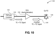
- FIG. 10 illustrates a silicon photonic integrated receiver with a PSR and combiner, SOA, and Ge PD, in accordance with various embodiments.
- Integrated receiver 1000 includes a combination PSR and combiner 1030 component that receives an optical signal and produces a TE + TE' signal 1032 that is received by an SOA 1034 to produce an amplified TE + TE' signal 1036.
- the amplified TE + TE' signal 1036 is then sent to a Ge PD 1038.
- the SOA 1034 is not required to be dual polarization or polarization insensitive; therefore, the SOA 1034 may be optimized for TE only amplification.
- the PSR and combiner 1030 splits the TE and TM (not shown) components of the input signal, rotates the polarization of the TM to a TE' signal, and then combines the TE and TE' together into one waveguide 1035 for amplification before conversion to an electrical signal at the Ge PD 1038.
- FIG. 11 illustrates a silicon photonic integrated receiver with a PSR and combiner, SOA, wavelength demultiplexer, and multiple Ge PDs, in accordance with various embodiments.
- Integrated wavelength division multiplexed receiver 1100 may include a PSR and combiner 1130, which may be similar to PSR and combiner 1030 of FIG. 10 .
- the PSR and combiner 1130 may receive one or more optical signals and produce signals on multiple wavelengths of a TE and TE' signals 1132.
- the SOA 1034 is used to amplify multiple wavelengths of the TE and TE' signals 1132 and produce the amplified multiple wavelengths 1036. These multiple wavelengths 1036 are then routed to a demultiplexer 1040 to separate the individual wavelengths 1142, 1144, 1146, 1148, which are then routed, respectively, to Ge PDs 1152, 1154, 1156, 1158.
- the SOA may be operated below saturation to limit signal distortion.
- receivers 800, 900, 1000, 1100 may be expanded to include multiple channels and/or signals on multiple wavelengths in each channel.
- an SOA 1134 may be used to amplify multiple wavelengths, with a demultiplexer 1140 separating out each individual wavelengths before proceeding to a Ge PD 1152, 1154, 1156, 1158.
- FIG. 12 illustrates a dual polarization transceiver with multiple SOAs, in accordance with various embodiments.
- Transceiver schematic 1200 shows a dual-polarization coherent transceiver that includes multiple options for SOA integration in both the transmitter and receiver portions of the schematic.
- the placement of an SOA in the coherent transceiver will dictate the requirements for the SOA. In a given placement, the SOA may or may not need to amplify data or have high output saturation power.
- Transceiver schematic 1200 is divided into three regions for SOA placement. Region 1200a includes SOA placement after an input to the transceiver 1200 and either before or after the splitter between the transmitter (region 1200b) and the receiver (region 1200c).
- Region 1200b includes SOA placement in the transmitter either after the IQ modulators or after the polarization rotator and combiner.
- Region 1200c includes SOA placement in the receiver before or after the polarization splitter and rotator. Embodiments of regions 1200a, 1200b, 1200c are described further below. These embodiments may be combined throughout the transceiver 1200 to form various embodiments.
- Region 1200a includes embodiments of SOA placed for optical signal power boosting at an input to the transceiver, and either before or after the split between the transmitter (region 1200b) or the receiver (region 1200c).
- the SOAs 1202, 1204, 1206, which may be placed in locations as shown, may be used to boost optical signal received from a tunable laser input 1208.
- the SOAs 1202, 1204, 1206 may require high saturation power in these configurations.
- the output power from the SOA will be 20dBm or 100mW in the case where the SOAs are after the splitter 1205. If SOAs 1204, 1206 are placed between the splitter 1205 for the two polarizations and the IQ modulators 1220, the output power from the SOAs 1204, 1206 will be 17dBm or 50mW. Both total power consumption of the SOA(s) and SOA reliability at high optical powers need to be considered for each SOA location option.
- Including more SOAs will inherently consume more electrical power, however operating at lower optical output power may be desirable from a component reliability standpoint, whether or not one option or the other is selected will depend on the overall system requirements.
- the two SOAs 1204, 1206 will generally consume more power.
- this design may not be optimal because operating at a lower optical power can improve reliability as the failure rates improve with lower drive current and lower optical power. Whether or not the improved reliability is needed is based on the system requirements for each application.
- the hybrid III-V/Si SOA is uniquely suited to achieve this high saturation power. Because the saturation power of an SOA is inversely proportional to the confinement factor, the overlap of the optical mode and the quantum well gain material, reducing the confinement factor increases saturation power.
- the III-V active region is bonded on top of a silicon waveguide and the confinement factor can be tuned by changing the width of the silicon waveguide. Widening the silicon waveguide pulls the mode down into the silicon waveguide and reduces the mode overlap with the quantum wells.
- the confinement factor can be optimized along the length of the SOA by tapering the Si waveguide width.
- TPA two-photon absorption
- the SOAs 1202, 1204, 1206 at the input of the transceiver may be amplifying continuous-wave light from the tunable laser, signal distortion from the SOA nonlinearities are not a concern.
- Region 1200b includes embodiments of SOAs 1222, 1224, 1226 placed in the transmitter 1200b either after IQ modulators 1220 or after the polarization rotator 1228 and polarization combiner 1230.
- the IQ modulators 1220 which in embodiments may be nested Si MZ modulators, may have a significant amount of loss, for example, on the order of 16dB. This loss, in addition to the inherent penalty from the modulation format, lowers the output power required from the SOAs 1222, 1224, 1226.
- the output power from the SOAs 1222, 1224, 1226 is not limited by two photon absorption (TPA), and the SOA 1222, 1224, 1226 gain can be higher compared to placement at the input of the transceiver.
- having an SOA 1222, 1224 for each polarization also offers the ability to balance the power between the two polarizations by tuning the gain in each SOA.
- a polarization independent SOA 1226 may be used or required if the SOA 1226 is placed after the polarization rotator 1228 and polarization combiner 1230 in the transmitter 1200b.
- SOAs 1222, 1224 optimized for amplifying a single polarization where compressively strained multiple quantum well gain material is commonly used an SOA 1226 with low polarization dependent gain may require different III-V gain material, such as bulk active material or tensile strained quantum wells, where the amount of strain is set to equalize the TE and TM gain.
- Using a single SOA 1226 to amplify both polarizations offers reduced power consumption compared to using two SOAs 1222, 1224 after each of the IQ modulators 1220. However, if there is only 1 SOA 1226 for both polarizations, there is a lack of ability to equalize power between the two polarizations.
- the performance transmitter 1200b with SOAs 1222, 1224, 1226 amplifying data is limited by amplified spontaneous emission (ASE) for low input powers and by nonlinear distortions at high input powers.
- the optimum range of input powers to the SOAs 1222, 1224, 1226 may be extracted from transmission system simulations with known or estimated link losses and SOA parameters to guide the decision on SOA placement within the transceiver 1200 among all the described options after modulation.
- One important parameter for SOAs is the noise figure (NF) that describes the amount of degradation from the spontaneous emission in the amplification process, or the ratio in decibel scale of the SNR (signal-to-noise ratio) at the input of the SOA to the SNR at the output of the SOA.
- NF noise figure
- a lower NF is desirable and indicates lower signal degradation during the amplification process.
- Region 1200c is a receiver that includes embodiments of SOAs 1242, 1244, 1246 placement in the receiver 1200c before or after the polarization splitter 1248 and polarization rotator 1250, 1251.
- a polarization independent SOA may be required if the SOA 1246 is placed before the polarization splitter 1248 and polarization rotator 1250.
- This configuration offers reduced power consumption compared to using two SOAs 1242, 1244, one for each polarization.
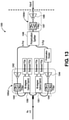
- FIG. 13 illustrates filter locations within a dual polarization transceiver with multiple SOAs to eliminate excess ASE, in accordance with various embodiments.
- Receiver portion 1300 may be similar to receiver 1200c of FIG. 12 , with SOA 1342, 1344, 1346 similar, respectively, to SOA 1242, 1244, 1246 of FIG. 12 .
- band pass filter 1343 may be placed between SOA 1342 and 90-degree optical hybrid 1350
- band pass filter 1345 may be placed between SOA 1344 and 90-degree optical hybrid 1351.
- a band pass filter 1347 may be placed between the SOA 1346 and polarization splitter 1348, which may be similar to polarization splitter 1248 of FIG. 12 .
- FIG. 14 schematically illustrates a computing device 1400 in accordance with one embodiment.
- the computing device 1400 may house a board such as motherboard 1402 (i.e., housing 1451).
- the motherboard 1402 may include a number of components, including but not limited to a processor 1404 and at least one communication chip 1406.
- the processor 1404 may be physically and electrically coupled to the motherboard 1402.
- the at least one communication chip 1406 may also be physically and electrically coupled to the motherboard 1402.
- communication chip 1406 is incorporated with the teachings of the present disclosure. That is, it includes one or more SOAs integrated within a photonics apparatus.
- the communication chip 1406 may be part of the processor 1404.
- one or more of the other enumerated elements may be incorporated with the teachings of the presented disclosure.
- computing device 1400 may include other components that may or may not be physically and electrically coupled to the motherboard 1402. These other components may include, but are not limited to, volatile memory (e.g., DRAM) 1420, nonvolatile memory (e.g., ROM) 1424, flash memory 1422, a graphics processor 1430, a digital signal processor (not shown), a crypto processor (not shown), a chipset 1426, an antenna 1428, a display (not shown), a touchscreen display 1432, a touchscreen controller 1446, a battery 1436, an audio codec (not shown), a video codec (not shown), a power amplifier 1441, a global positioning system (GPS) device 1440, a compass 1442, an accelerometer (not shown), a gyroscope (not shown), a speaker 1450, a camera 1452, and a mass storage device (such as hard disk drive, compact disk (CD), digital versatile disk (DVD), and so forth) (not shown).
- volatile memory e.g.
- FIG. 14 may include a microphone, a filter, an oscillator, a pressure sensor, or an RFID chip.
- one or more of the package assembly components 1455 may include one or more SOAs integrated within a photonics apparatus, as discussed herein.
- the communication chip 1406 may enable wireless communications for the transfer of data to and from the computing device 1400.
- wireless and its derivatives may be used to describe circuits, devices, systems, processes, techniques, communications channels, etc., that may communicate data through the use of modulated electromagnetic radiation through a non-solid medium. The term does not imply that the associated devices do not contain any wires, although in some embodiments they might not.
- the communication chip 1406 may implement any of a number of wireless standards or protocols, including but not limited to Institute for Electrical and Electronic Engineers (IEEE) standards including Wi-Fi (IEEE 802.11 family), IEEE 802.16 standards (e.g., IEEE 802.16-2005 Amendment), Long-Term Evolution (LTE) project along with any amendments, updates, and/or revisions (e.g., advanced LTE project, ultra mobile broadband (UMB) project (also referred to as "3GPP2”), etc.).
- IEEE 802.16 compatible BWA networks are generally referred to as WiMAX networks, an acronym that stands for Worldwide Interoperability for Microwave Access, which is a certification mark for products that pass conformity and interoperability tests for the IEEE 802.16 standards.
- the communication chip 1406 may operate in accordance with a Global System for Mobile Communication (GSM), General Packet Radio Service (GPRS), Universal Mobile Telecommunications System (UMTS), High Speed Packet Access (HSPA), Evolved HSPA (E-HSPA), or LTE network.
- GSM Global System for Mobile Communication
- GPRS General Packet Radio Service
- UMTS Universal Mobile Telecommunications System
- High Speed Packet Access HSPA
- E-HSPA Evolved HSPA
- LTE LTE network.
- the communication chip 1406 may operate in accordance with Enhanced Data for GSM Evolution (EDGE), GSM EDGE Radio Access Network (GERAN), Universal Terrestrial Radio Access Network (UTRAN), or Evolved UTRAN (E-UTRAN).
- EDGE Enhanced Data for GSM Evolution
- GERAN GSM EDGE Radio Access Network
- UTRAN Universal Terrestrial Radio Access Network
- E-UTRAN Evolved UTRAN
- the communication chip 1406 may operate in accordance with Code Division Multiple Access (CDMA), Time Division Multiple Access (TDMA), Digital Enhanced Cordless Telecommunications (DECT), Evolution-Data Optimized (EV-DO), derivatives thereof, as well as any other wireless protocols that are designated as 3G, 4G, 5G, and beyond.
- CDMA Code Division Multiple Access
- TDMA Time Division Multiple Access
- DECT Digital Enhanced Cordless Telecommunications
- EV-DO Evolution-Data Optimized
- derivatives thereof as well as any other wireless protocols that are designated as 3G, 4G, 5G, and beyond.
- the communication chip 1406 may operate in accordance with other wireless protocols in other embodiments.
- the communication chip 1406 may include one or more SOAs integrated within a photonics apparatus, as discussed herein.
- the computing device 1400 may include a plurality of communication chips 1406.
- a first communication chip 1406 may be dedicated to shorter range wireless communications such as Wi-Fi and Bluetooth and a second communication chip 1406 may be dedicated to longer range wireless communications such as GPS, EDGE, GPRS, CDMA, WiMAX, LTE, Ev-DO, and others.
- the processor 1404 of the computing device 1400 may include a die in a package assembly such as, for example, one or more SOAs within a photonics apparatus, as described herein.
- the term "processor” may refer to any device or portion of a device that processes electronic data from registers and/or memory to transform that electronic data into other electronic data that may be stored in registers and/or memory.
- the computing device 1400 may be a laptop, a netbook, a notebook, an ultrabook, a smartphone, a tablet, a personal digital assistant (PDA), an ultra mobile PC, a mobile phone, a desktop computer, a server, a printer, a scanner, a monitor, a set-top box, an entertainment control unit, a digital camera, a portable music player, or a digital video recorder.
- the computing device 1400 may be any other electronic device that processes data, for example, an all-in-one device such as an all-in-one fax or printing device.
- Various embodiments may include any suitable combination of the above-described embodiments including alternative (or) embodiments of embodiments that are described in conjunctive form (and) above (e.g., the "and” may be “and/or”).
- some embodiments may include one or more articles of manufacture (e.g., non-transitory computer-readable media) having instructions, stored thereon, that when executed result in actions of any of the above-described embodiments.
- some embodiments may include apparatuses or systems having any suitable means for carrying out the various operations of the above-described embodiments.
Landscapes
- Physics & Mathematics (AREA)
- Electromagnetism (AREA)
- Optics & Photonics (AREA)
- General Physics & Mathematics (AREA)
- Condensed Matter Physics & Semiconductors (AREA)
- Engineering & Computer Science (AREA)
- Computer Networks & Wireless Communication (AREA)
- Signal Processing (AREA)
- Microelectronics & Electronic Packaging (AREA)
- Optical Modulation, Optical Deflection, Nonlinear Optics, Optical Demodulation, Optical Logic Elements (AREA)
- Semiconductor Lasers (AREA)
Applications Claiming Priority (1)
| Application Number | Priority Date | Filing Date | Title |
|---|---|---|---|
| US17/024,342 US20210006044A1 (en) | 2020-09-17 | 2020-09-17 | Integrated semiconductor optical amplifiers for silicon photonics |
Publications (1)
| Publication Number | Publication Date |
|---|---|
| EP3972156A1 true EP3972156A1 (fr) | 2022-03-23 |
Family
ID=74065607
Family Applications (1)
| Application Number | Title | Priority Date | Filing Date |
|---|---|---|---|
| EP21190283.8A Pending EP3972156A1 (fr) | 2020-09-17 | 2021-08-09 | Amplificateurs optiques intégrés à semi-conducteurs pour la photonique au silicium |
Country Status (3)
| Country | Link |
|---|---|
| US (2) | US20210006044A1 (fr) |
| EP (1) | EP3972156A1 (fr) |
| CN (1) | CN114205000A (fr) |
Families Citing this family (13)
| Publication number | Priority date | Publication date | Assignee | Title |
|---|---|---|---|---|
| US11557875B2 (en) | 2020-07-24 | 2023-01-17 | Arista Networks, Inc. | Network device with optical communication interface |
| US11594854B2 (en) | 2020-07-24 | 2023-02-28 | Arista Networks, Inc. | Optical communication interface |
| JP2022114537A (ja) * | 2021-01-27 | 2022-08-08 | 富士通株式会社 | 波長分波装置、光送受信器、光回路、及び波長分波制御方法 |
| US12424823B2 (en) | 2021-06-03 | 2025-09-23 | Intel Corporation | Multi-wavelength distributed feedback laser |
| US12328147B2 (en) | 2021-06-22 | 2025-06-10 | Intel Corporation | System, apparatus and method for optical intensity modulation with direct detection using local oscillator |
| US12461396B2 (en) | 2021-06-25 | 2025-11-04 | Intel Corporation | Heating of thermo-optic device |
| JP7580606B2 (ja) * | 2021-06-28 | 2024-11-11 | 三菱電機株式会社 | 光半導体装置 |
| US11442235B1 (en) | 2021-07-29 | 2022-09-13 | Hewlett Packard Enterprise Development Lp | Optical system including optical devices having in-situ capacitive structures |
| US11927819B2 (en) | 2021-11-10 | 2024-03-12 | Hewlett Packard Enterprise Development Lp | Optical device having a light-emitting structure and a waveguide integrated capacitor to monitor light |
| US12009912B2 (en) | 2022-03-23 | 2024-06-11 | Taiwan Semiconductor Manufacturing Company, Ltd. | WDM channel reassignment |
| CN115133996B (zh) * | 2022-08-31 | 2022-11-04 | 华中科技大学 | 增益钳制双向半导体光放大器的中长距双工同源相干系统 |
| US20240288749A1 (en) * | 2023-02-17 | 2024-08-29 | Infinera Corporation | Photonic integrated circuit including semiconductor optical amplifiers |
| WO2025161114A1 (fr) * | 2024-01-30 | 2025-08-07 | 青岛海信宽带多媒体技术有限公司 | Module optique |
Citations (6)
| Publication number | Priority date | Publication date | Assignee | Title |
|---|---|---|---|---|
| US20130279910A1 (en) * | 2012-04-18 | 2013-10-24 | Infinera Corporation | Banded Semiconductor Optical Amplifier |
| EP2730958A1 (fr) * | 2012-11-07 | 2014-05-14 | Alcatel-Lucent | Détecteur cohérent amplifié |
| US9647426B1 (en) * | 2013-06-28 | 2017-05-09 | Aurrion, Inc. | Polarization insensitive colorless optical devices |
| US20190049743A1 (en) * | 2017-08-08 | 2019-02-14 | Fujitsu Limited | Optical amplifier and optical switch device |
| US20190342010A1 (en) * | 2018-05-07 | 2019-11-07 | Infinera Corporation | Spare channels on photonic integrated circuits and in photonic integrated circuit modules and systems |
| US10754091B1 (en) * | 2019-03-18 | 2020-08-25 | Inphi Corporation | Integrated coherent optical transceiver, light engine |
Family Cites Families (3)
| Publication number | Priority date | Publication date | Assignee | Title |
|---|---|---|---|---|
| US20180351684A1 (en) * | 2016-11-15 | 2018-12-06 | Infinera Corparation | Optical modules having an improved optical signal to noise ratio |
| US10509243B2 (en) * | 2017-03-15 | 2019-12-17 | Elenion Technologies, Llc | Bias control of optical modulators |
| JP6919557B2 (ja) * | 2017-12-26 | 2021-08-18 | 住友電気工業株式会社 | 光90度ハイブリッド集積回路 |
-
2020
- 2020-09-17 US US17/024,342 patent/US20210006044A1/en not_active Abandoned
-
2021
- 2021-08-09 EP EP21190283.8A patent/EP3972156A1/fr active Pending
- 2021-08-17 CN CN202110941378.1A patent/CN114205000A/zh active Pending
-
2024
- 2024-07-29 US US18/787,825 patent/US20240388067A1/en active Pending
Patent Citations (6)
| Publication number | Priority date | Publication date | Assignee | Title |
|---|---|---|---|---|
| US20130279910A1 (en) * | 2012-04-18 | 2013-10-24 | Infinera Corporation | Banded Semiconductor Optical Amplifier |
| EP2730958A1 (fr) * | 2012-11-07 | 2014-05-14 | Alcatel-Lucent | Détecteur cohérent amplifié |
| US9647426B1 (en) * | 2013-06-28 | 2017-05-09 | Aurrion, Inc. | Polarization insensitive colorless optical devices |
| US20190049743A1 (en) * | 2017-08-08 | 2019-02-14 | Fujitsu Limited | Optical amplifier and optical switch device |
| US20190342010A1 (en) * | 2018-05-07 | 2019-11-07 | Infinera Corporation | Spare channels on photonic integrated circuits and in photonic integrated circuit modules and systems |
| US10754091B1 (en) * | 2019-03-18 | 2020-08-25 | Inphi Corporation | Integrated coherent optical transceiver, light engine |
Non-Patent Citations (1)
| Title |
|---|
| KASPAR P ET AL: "Hybrid III-V/silicon SOA for photonic integrated circuits", 20141113, vol. 9277, 13 November 2014 (2014-11-13), pages 927708 - 927708, XP060043581, DOI: 10.1117/12.2074617 * |
Also Published As
| Publication number | Publication date |
|---|---|
| US20240388067A1 (en) | 2024-11-21 |
| CN114205000A (zh) | 2022-03-18 |
| US20210006044A1 (en) | 2021-01-07 |
Similar Documents
| Publication | Publication Date | Title |
|---|---|---|
| US20240388067A1 (en) | Integrated semiconductor optical amplifiers for silicon photonics | |
| KR102503881B1 (ko) | 테라헤르츠 신호 송신 장치 및 이를 이용한 테라헤르츠 신호 송신 방법 | |
| US10855376B1 (en) | Reflection engineering / wavelength division multiplexing (WDM) geometric optical isolator | |
| US11689291B2 (en) | Systems and methods for optical full-field transmission using photonic integration | |
| US8977121B2 (en) | Spatial domain based multi dimensional coded modulation for multi Tb per second serial optical transport networks | |
| US8705983B2 (en) | Radio frequency optical communication system | |
| Going et al. | 1.00 (0.88) Tb/s per wave capable coherent multi-channel transmitter (receiver) InP-based PICs with hybrid integrated SiGe electronics | |
| WO2020207360A1 (fr) | Source de lumière en peigne de fréquence optique et procédé de génération de peigne de fréquence optique | |
| CA2814578A1 (fr) | Procede et systeme pour recepteurs optiques | |
| US20200252133A1 (en) | Photonic transmitter with optical amplifier | |
| Takechi et al. | 64 GBaud high-bandwidth micro intradyne coherent receiver using high-efficiency and high-speed InP-based photodetector integrated with 90° hybrid | |
| US20210175974A1 (en) | Optical coherent transmitter on a silicon chip | |
| Shindo et al. | High modulated output power over 9.0 dBm with 1570-nm wavelength SOA assisted extended reach EADFB laser (AXEL) | |
| Tatsumi et al. | A compact low-power 224-Gb/s DP-16QAM modulator module with InP-based modulator and linear driver ICs | |
| Ozaki et al. | 500-Gb/s/λ operation of ultra-low power and low-temperature-dependence InP-based high-bandwidth coherent driver modulator | |
| Umezawa et al. | Multi-core based 94-GHz radio and power over fiber transmission using 100-GHz analog photoreceiver | |
| Chen et al. | Inp cdm and icr enabled 128gbaud/dp-16qam-ps and 120gbaud/dp-qpsk long-haul transmission | |
| Kono et al. | Compact and low power DP-QPSK modulator module with InP-based modulator and driver ICs | |
| Li et al. | SOA enabled self-homodyne coherent bidirectional transmission for metro-datacenter interconnects | |
| US20240372623A1 (en) | Multi-node, multi-stream photonic integrated circuit-based free-space optical communication device | |
| Poirier et al. | InP integrated coherent transmitter for 100 Gb/s DP-QPSK transmission | |
| EP3172850B1 (fr) | Émetteur-récepteur optique multicouche électroabsorbant à cavité verticale et à émission par la surface | |
| US20240291566A1 (en) | Photonic integrated circuit including semiconductor optical amplifiers | |
| Zhou et al. | Characterizations of semiconductor optical amplifiers for 64Gbaud 16-64QAM coherent optical transceivers | |
| Griffin | InP-based high-speed transponder |
Legal Events
| Date | Code | Title | Description |
|---|---|---|---|
| PUAI | Public reference made under article 153(3) epc to a published international application that has entered the european phase |
Free format text: ORIGINAL CODE: 0009012 |
|
| STAA | Information on the status of an ep patent application or granted ep patent |
Free format text: STATUS: THE APPLICATION HAS BEEN PUBLISHED |
|
| AK | Designated contracting states |
Kind code of ref document: A1 Designated state(s): AL AT BE BG CH CY CZ DE DK EE ES FI FR GB GR HR HU IE IS IT LI LT LU LV MC MK MT NL NO PL PT RO RS SE SI SK SM TR |
|
| STAA | Information on the status of an ep patent application or granted ep patent |
Free format text: STATUS: REQUEST FOR EXAMINATION WAS MADE |
|
| 17P | Request for examination filed |
Effective date: 20220923 |
|
| RBV | Designated contracting states (corrected) |
Designated state(s): AL AT BE BG CH CY CZ DE DK EE ES FI FR GB GR HR HU IE IS IT LI LT LU LV MC MK MT NL NO PL PT RO RS SE SI SK SM TR |
|
| STAA | Information on the status of an ep patent application or granted ep patent |
Free format text: STATUS: EXAMINATION IS IN PROGRESS |
|
| 17Q | First examination report despatched |
Effective date: 20231213 |