EP3973251B1 - Sensormodul und verfahren zur bereitstellung eines sensormodul-signals - Google Patents
Sensormodul und verfahren zur bereitstellung eines sensormodul-signals Download PDFInfo
- Publication number
- EP3973251B1 EP3973251B1 EP20726435.9A EP20726435A EP3973251B1 EP 3973251 B1 EP3973251 B1 EP 3973251B1 EP 20726435 A EP20726435 A EP 20726435A EP 3973251 B1 EP3973251 B1 EP 3973251B1
- Authority
- EP
- European Patent Office
- Prior art keywords
- signal
- sensor
- sensor module
- processed
- sensor signal
- Prior art date
- Legal status (The legal status is an assumption and is not a legal conclusion. Google has not performed a legal analysis and makes no representation as to the accuracy of the status listed.)
- Active
Links
Images
Classifications
-
- G—PHYSICS
- G01—MEASURING; TESTING
- G01D—MEASURING NOT SPECIALLY ADAPTED FOR A SPECIFIC VARIABLE; ARRANGEMENTS FOR MEASURING TWO OR MORE VARIABLES NOT COVERED IN A SINGLE OTHER SUBCLASS; TARIFF METERING APPARATUS; MEASURING OR TESTING NOT OTHERWISE PROVIDED FOR
- G01D3/00—Indicating or recording apparatus with provision for the special purposes referred to in the subgroups
- G01D3/08—Indicating or recording apparatus with provision for the special purposes referred to in the subgroups with provision for safeguarding the apparatus, e.g. against abnormal operation, against breakdown
-
- G—PHYSICS
- G01—MEASURING; TESTING
- G01L—MEASURING FORCE, STRESS, TORQUE, WORK, MECHANICAL POWER, MECHANICAL EFFICIENCY, OR FLUID PRESSURE
- G01L19/00—Details of, or accessories for, apparatus for measuring steady or quasi-steady pressure of a fluent medium insofar as such details or accessories are not special to particular types of pressure gauges
- G01L19/0092—Pressure sensor associated with other sensors, e.g. for measuring acceleration or temperature
Definitions
- the present invention relates to a sensor module and a method for providing a sensor module signal comprising information representative of a physical quantity measured by means of the sensor module.
- sensor modules for providing a sensor module signal representative of a physical quantity measured by means of the sensor module typically comprise a sensor for providing a sensor signal representative of the physical quantity and a processing device for generating the sensor module signal based on the sensor signal.
- the signal processing may comprise a calibration of an analog sensor signal, a filtering (e.g. lowpass filtering) and/or an analog/digital conversion of the signal.
- Such a sensor module can be used for example in a vehicle for measuring physical quantities as e.g. a temperature, a pressure etc.
- sensor systems with high safety or OBD requirements often use redundant sensor signal acquisition and processing by using two sensors and two processing devices. This technique increases the likelihood that the measured physical quantity (e.g. temperature, pressure etc.) can continue to be observed even with sensor errors.
- measured physical quantity e.g. temperature, pressure etc.
- redundant sensor signal acquisition and processing in some cases allows the detection of errors within the signal chain from each sensor to a receiving device that receives the sensor module signal.
- the redundant signal paths are often implemented in a common chip or package.
- a common output stage is usually used, i.e. the redundantly detected and processed sensor signals (comprising at least a first and a second sensor signal) are transmitted on a common (usually digital) signal line to a receiving device.
- Such an output stage can comprise a control device for generating the (e.g. digital) sensor module signal based on the processed first sensor signal and the processed second sensor signal, and e.g. an output driver that forms an interface for connection of the sensor module to a (e.g. digital) transmission line running to the receiving device.
- a control device for generating the (e.g. digital) sensor module signal based on the processed first sensor signal and the processed second sensor signal
- an output driver that forms an interface for connection of the sensor module to a (e.g. digital) transmission line running to the receiving device.
- the sensor module signal, the processed first sensor signal and the processed second sensor signal are checked for coherency, and a check result signal representative of a result of this check is provided.
- the invention it is advantageously realized a redundant measurement of the physical quantity by means of the (at least) first and second sensors, wherein the information about this physical quantity can be transmitted via a common interface (and a common transmission line) to a receiving device, wherein the diagnostic coverage for possible errors is improved.
- a further redundancy-generating device is integrated in the sensor module.
- the checking device checks the sensor module signal, the processed first sensor signal and the processed second sensor signal for coherency by checking whether the sensor module signal has plausibility in view of the processed first and second sensor signals and thusly checks an error-free transmission of the first and second processed sensor signals from the first and second processing devices to the control device, as well as an error-free function of the control device.
- the checking device can for example be adapted to compare values (e.g. data values) regarding the physical quantities measured by the first and second sensors as generated by the control device and thus to be transmitted with the desired output values (as apparent from the processed first and second sensor signals).
- values e.g. data values
- the check result signal representative of the result of the check is transferable or is transfered to a receiving device via a transmission line independent from a transmission line provided for the sensor module signal.
- both independent transmission lines may run in a commonly used transmission hardware as e.g. an electrical cable.
- the checking device is adapted to provide the check result signal at an (electrical) output terminal of the sensor module, which is provided separate from an (electrical) output terminal of the sensor module used for the sensor module signal.
- an incoherence detected by means of the check e.g. by detecting a deviation as a result of the above mentioned comparison
- it can be provided to modify the content of a digital sensor module signal by inserting or setting an error flag in a respective data element, or by intentional falsification of a checksum and/or a running counter in a respective data element of the digital sensor module signal.
- the first and second sensors are designed for providing analog signals as e.g. an analog temperature signal or an analog pressure signal.
- the sensor module can advantageously be adapted to provide for a digital processing of the measured information (first and second sensor signals).
- the digital processing comprises a filtering, e.g. lowpass filtering.
- each of the above mentioned first digital processing device and second digital processing device is adapted to receive a processing clock signal and has a digital output register for providing the processed first sensor signal and the processed second sensor signal, respectively, in form of data updated in accordance with the processing clock signal.
- each of the first and second digital processing devices is adapted to receive a second processing clock signal and reads digital output values from outputs of the ADCs in accordance with the second processing clock signal.
- the clock frequency of the second processing clock signal may be chosen higher than that of the processing clock signal (e.g. by a factor of "n", wherein n is an integer in the range of 5 to 50).
- the digital processing devices can foresee for example a calculation of average values (e.g. moving averages) of the ADC outputs, wherein these average values are used in a subsequent calculation of the digital signals SS1', SS2'.
- control device can be adapted to generate the sensor module signal as an analog signal (e.g. analog voltage signal), or to convert a digitally generated sensor module signal into an analog signal, so that finally an analog module signal is provided (at an output terminal or output interface) by the sensor module.
- control device of the sensor module preferably comprises an output driver for amplification of the analog sensor module signal.
- control device can be adapted to generate the sensor module signal comprising information representative of the physical quantity (e.g. a pressure or a temperature), which information has been determined by the control device based on the processed first sensor signal and the processed second sensor signal, without providing both the information representative of the processed first sensor signal and the information representative of the processed second sensor signal in the outputted sensor module signal.
- the sensor module signal comprising information representative of the physical quantity (e.g. a pressure or a temperature), which information has been determined by the control device based on the processed first sensor signal and the processed second sensor signal, without providing both the information representative of the processed first sensor signal and the information representative of the processed second sensor signal in the outputted sensor module signal.
- control device is adapted to generate the sensor module signal in form of digital data according to a customer specific protocol.
- this protocol used to generate the sensor module signal in form of digital data is a common standard protocol, as e.g. the SENT ("Single Edge Nibble Transmission") protocol.
- SENT Single Edge Nibble Transmission
- CAN Controller Area Network
- LIN Local Interconnect Network
- a method for providing a sensor module signal comprising information representative of a physical quantity measured by means of a sensor module comprises
- the first and second sensor signals can be provided as analog signals (e.g. analog voltage signals).
- the first digitally processing and the second digitally processing is in each case conducted with use of a processing clock signal, wherein the processed first sensor signal and the processed second sensor signal, respectively, is provided in form of data, which are updated in accordance with the respective processing clock signal.
- the processing clock signals for the first and second digital processing devices have the same clock frequency.
- the processing clock signals are not generated by a common clock generator (oscillator). Rather, for redundancy reason, it is preferred to use independent clock generators for different digital processing devices.
- the generation of the sensor module signal provides the sensor module signal in form of digital data at least containing a data element representative of the processed first sensor signal and a data element representative of the processed second sensor signal.
- the generation of the sensor module signal provides the sensor module signal in form of digital data containing at least one data element representative of the physical quantity measured by means of the sensor module and at least one data element constituting a checksum of the first mentioned data element and/or constituting a running counter.
- the generation of the sensor module signal provides the sensor module signal in form of digital data according to a standard protocol, as e.g. the SENT protocol.
- the devices used for processing digital signals can be implemented by means of a software-controlled computing device (e.g. microcontroller) and/or a PLD, CPLD or FPGA device.
- a software-controlled computing device e.g. microcontroller
- PLD e.g. CMOS
- CPLD CPLD
- FPGA field-programmable gate array
- these devices for processing digital signals are implemented as ASIC ("application-specific integrated circuit"), in particular e.g. via semiconductor masks hardwired logic fields.
- the present invention can be used in many fields in which a sensor system comprising a sensor module and an associated receiving device is needed, wherein the system has to fulfill high safety requirements.
- the first and second sensor signals each are representative of a pressure, e.g. a pressure of an operational fluid of a drive system of a vehicle (e.g. oil in an internal combustion engine).
- a pressure e.g. a pressure of an operational fluid of a drive system of a vehicle (e.g. oil in an internal combustion engine).
- the first and second sensor signals each are representative of a pressure within a battery housing accommodating at least one battery cell.
- each of the first and second sensors is a pressure sensor formed by a microelectromechanical system (MEMS).
- MEMS microelectromechanical system
- the first and second sensor signals each are representative of a temperature within a battery housing accommodating at least one battery cell.
- Such a battery housing together with the battery cell(s) can for example form a battery module of a vehicle, wherein the battery module can provide for example a rechargeable electrical energy source for supplying energy for the propulsion of the vehicle (e.g. electric vehicle, hybrid vehicle, etc.).
- the battery module can provide for example a rechargeable electrical energy source for supplying energy for the propulsion of the vehicle (e.g. electric vehicle, hybrid vehicle, etc.).
- An increase in pressure of the battery housing surrounding the battery cell(s) of electrified vehicles can be used to draw conclusions about malfunctions of the battery cell(s). For example, a temperature increase may lead to outgassing within a battery cell and thus to a significant increase in pressure and/or temperature and would thus be an indicator of impending destruction of the battery cell.
- a sensor module or a sensor system comprising such sensor module as described therein for dectecting a pressure (or a temperature) in a battery housing surrounding one or more battery cells of an electrified vehicle as for example a hybrid vehicle.
- the system can be provided for example to detect a pressure or a temperature within a battery housing accommodating at least one battery cell.
- the receiving device can be adapted to conduct a plausibility check and/or an error recognition by means of analysing the received sensor module signal.
- analysing can comprise a calculation of a likelihood for plausibility of the sensor module signal and/or a likelihood of a particular error (e.g. failure or defect of one of the sensors) by means of a software-controlled computing device (e.g. microcontroller).
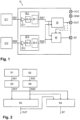
- the sensor module 10 further comprises a first processing device 20-1 for processing the signal SS1 and outputting a processed first sensor signal SS1', and a second processing device 20-2 for processing the signal SS2 and outputting a processed second sensor signal SS2'.
- the processing conducted by the processing devices 20-1, 20-2 in each case comprises a calibration, a filtering (e.g. a lowpass filtering), and an analog/digital conversion.
- a filtering e.g. a lowpass filtering
- each of the processing devices 20-1 and 20-2 comprises a calibrating amplifier 22-1 and 22-2, respectively, an ADC (analog/digital converter) 24-1 and 24-2, respectively, and a digital processing device 26-1 and 26-2, respectively.
- the calibrating amplifiers 22-1, 22-2 provide for respective calibrations of the signals SS1, SS2 when supplying them to the ADCs 24-1, 24-2, such that, for example, in a normal operation of the sensors 12-1, 12-2, the amplified versions of the signals SS1 and SS2 are identical or at least approximately identical.
- the ADCs 24-1, 24-2 provide for analog/digital conversion of the calibrated versions of the signals SS1, SS2 and supply digital representations thereof to the digital processing devices 26-1, 26-2.
- the digital processing devices 26-1, 26-2 provide processed digital first and second sensor signals SS1' and SS2', which form output signals of the respective processing devices 20-1, 20-2, as shown in Fig. 1 .
- the above mentioned calibration of the signals SS1, SS2 can alternatively or additionally be provided by means of the digital processing devices 26-1, 26-2.
- each of the first and second digital processing devices 26-1, 26-2 is adapted to receive a processing clock signal and has a digital output register for providing the processed first sensor signal SS1' and the processed second sensor signal SS2', respectively, in form of data updated in accordance with the processing clock signal.
- the sensor module 10 further comprises a control device 30 for generating the sensor module signal OUT based on the signals SS1' and SS2', which are supplied by the respective digital processing devices 26-1, 26-2 to the control device 30.
- the control device 30 receives a controlling clock signal and has a digital input register for retrieving input data from said output register of the processing devices 20-1, 20-2 in accordance with the controlling clock signal.
- the controlling clock signal has the same frequency as the processing clock signal.
- the control device 30 (e.g. microcontroller, or e.g. hardwired logic circuitry, preferably implemented as an ASIC) has a computing unit for processing the signals SS1' and SS2', which are inputted in form of digital data retrieved from the output registers of the processing devices 20-1, 20-2. The processing is accomplished by conducting a predefined algorithm. Further, based on the result of the processing, the computing unit generates (calculates) the sensor module signal OUT in form of digital data according to a predefined protocol for data transmission (e.g. SENT protocol).
- a predefined protocol for data transmission e.g. SENT protocol
- the digital data constituting the signal OUT at least contain a data element representative of digital values of the processed first sensor signal SS1' and a data element representative of digital values of the processed second sensor signal SS2'.
- the sensor module 10 shown in Fig. 1 may be modified by supplementing one or more further sensors (as the shown sensors 12-1, 12-2), supplementing a corresponding plurality of processing devices (as the shown processing devices 20-1, 20-2), and using a control unit (instead of the shown control unit 30) capable for processing the resulting plurality of signals supplied to the control unit (as the shown signals SS1', SS2').
- the signal OUT contains also data elements representing a checksum of the data elements representative of the signals SS1', SS2' and data elements constituting a running counter.
- Such transmission and/or processing errors can be based, for example, on semiconductor defects, drifting or failed clock signals, runtime errors in a digital part.
- errors that affect SS1'and SS2' as part of the OUT signal in the same way e.g. freezing both channel's information, or common offsets or falsification
- the sensor module 10 further comprises a checking device 40 for checking the sensor module signal OUT, the processed first sensor signal SS1' and the processed second sensor signal SS2' for coherency, and for providing a check result signal "EF" representative of a result of the check.
- a checking device 40 for checking the sensor module signal OUT, the processed first sensor signal SS1' and the processed second sensor signal SS2' for coherency, and for providing a check result signal "EF" representative of a result of the check.
- the signal OUT can also be tapped by the checking device 40 from an output of the sensor module 10, such that the signal OUT tapped for the purpose of coherency check is identical to the signal OUT as running over the transmission line to the receiving device.
- a reaction in such error condition can be for example an insertion of error flags into the digital output signal OUT.
- Alternative reactions can be for example a falsification of checksums and/or running counters contained in the output signal OUT.
- a further reaction may be a prevention of the sending of a current data telegram or future data telgrams from the sensor module 10 to the receiving device.
- Fig. 2 shows a schematic flowchart of a method according to the invention (and as implemented e.g. by the sensor module 10 in Fig. 1 ), comprising: providing a first sensor signal SS1 (step S1) and providing a second sensor signal SS2 (step S2); processing the first sensor signal SS1 (step S3) and processing the second sensor signal SS2 (step S4) to provide processed first and second sensor signals SS1' and SS2'; generating a sensor module signal OUT (step S5) based on the processed first and second sensor signals SS1' and SS2'; and checking the sensor module signal OUT, the processed first and second sensor signals SS1', SS2' for coherency to provide a check result signal "EF" representative of a result of the check.
Landscapes
- Physics & Mathematics (AREA)
- General Physics & Mathematics (AREA)
- Chemical & Material Sciences (AREA)
- Analytical Chemistry (AREA)
- Arrangements For Transmission Of Measured Signals (AREA)
- Testing Or Calibration Of Command Recording Devices (AREA)
Claims (10)
- Sensormodul (10) zum Bereitstellen eines Sensormodulsignals (OUT), das Informationen aufweist, die eine mithilfe des Sensormoduls (10) gemessene physikalische Größe repräsentieren, wobei das Sensormodul aufweist- einen ersten Sensor (12-1) zum Bereitstellen eines ersten Sensorsignals (SS1), das die physikalische Größe repräsentiert,- eine erste Verarbeitungsvorrichtung (20-1) zum Verarbeiten des ersten Sensorsignals (SS1), um ein verarbeitetes erstes Sensorsignal (SS1') bereitzustellen,- einen zweiten Sensor (12-2) zum Bereitstellen eines zweiten Sensorsignals (SS2), das die physikalische Größe repräsentiert,- eine zweite Verarbeitungsvorrichtung (20-2) zum Verarbeiten des zweiten Sensorsignals (SS2), um ein verarbeitetes zweites Sensorsignal (SS2') bereitzustellen,- eine Steuervorrichtung (30) zum Erzeugen des Sensormodulsignals (OUT) auf der Grundlage des verarbeiteten ersten Sensorsignals (SS1') und des verarbeiteten zweiten Sensorsignals (SS2'),- eine Prüfvorrichtung (40) zum Prüfen des Sensormodulsignals (OUT), des verarbeiteten ersten Sensorsignals (SS1') und des verarbeiteten zweiten Sensorsignals (SS2') auf Kohärenz, indem geprüft wird, ob das Sensormodulsignal (OUT) eine Plausibilität hinsichtlich des verarbeiteten ersten und des verarbeiteten zweiten Sensorsignals (SST, SS2') aufweist, und indem auf diese Weise eine fehlerfreie Übertragung des verarbeiteten ersten und des verarbeiteten zweiten Sensorsignals (SST, SS2') von der ersten und der zweiten Verarbeitungsvorrichtung (20,1,20-2) zu der Steuervorrichtung (30) geprüft wird und indem eine fehlerfreie Funktion der Steuervorrichtung (30) geprüft wird, und zum Bereitstellen eines Prüfergebnissignals (EF), das ein Ergebnis der Prüfung repräsentiert.
- Sensormodul (10) nach Anspruch 1, wobei der erste und der zweite Sensor (12-1, 12-2) zum Bereitstellen von analogen Signalen ausgelegt sind.
- Sensormodul (10) nach Anspruch 2,wobei die erste Verarbeitungsvorrichtung (20-1) einen ersten Kalibrierverstärker (22-1) zum Bereitstellen eines verstärkten ersten Sensorsignals und einen ersten ADC (24-1) für eine Analog/Digital-Wandlung des verstärkten ersten Sensorsignals in ein digitales erstes Sensorsignal aufweist, undwobei die zweite Verarbeitungsvorrichtung (20-2) einen zweiten Kalibrierverstärker (22-2) zum Bereitstellen eines verstärkten zweiten Sensorsignals und einen zweiten ADC (24-1) für eine Analog/Digital-Wandlung des verstärkten zweiten Sensorsignals in ein digitales zweites Sensorsignal aufweist.
- Sensormodul (10) nach Anspruch 3,wobei die erste Verarbeitungsvorrichtung (20-1) ferner eine erste digitale Verarbeitungsvorrichtung (26-1) zum digitalen Verarbeiten des digitalen ersten Sensorsignals aufweist, um das verarbeitete erste Sensorsignal (SS1') bereitzustellen, undwobei die zweite Verarbeitungsvorrichtung (20-2) ferner eine zweite digitale Verarbeitungsvorrichtung (26-2) zum digitalen Verarbeiten des digitalen zweiten Sensorsignals aufweist, um das verarbeitete zweite Sensorsignal (SS2') bereitzustellen.
- Sensormodul (10) nach Anspruch 4, wobei jede der ersten digitalen Verarbeitungsvorrichtung (26-1) und der zweiten digitalen Verarbeitungsvorrichtung (26-2) geeignet ist, um ein Verarbeitungstaktsignal zu empfangen, und ein digitales Ausgangsregister zum Bereitstellen des verarbeiteten ersten Sensorsignals (SS1') bzw. des verarbeiteten zweiten Sensorsignals (SS2') in Form von Daten aufweist, die gemäß dem Verarbeitungstaktsignal aktualisiert werden.
- Sensormodul (10) nach einem der vorhergehenden Ansprüche, wobei die Steuervorrichtung (30) geeignet ist zum Erzeugen des Sensormodulsignals (OUT) in Form von digitalen Daten, die mindestens ein Datenelement, welches das verarbeitete erste Sensorsignal (SS1') repräsentiert, und ein Datenelement enthalten, welches das verarbeitete zweite Sensorsignal (SS2') repräsentiert.
- Sensormodul (10) nach einem der vorhergehenden Ansprüche, wobei die Steuervorrichtung (30) geeignet ist zum Erzeugen des Sensormodulsignals (OUT) in Form von digitalen Daten, die mindestens ein Datenelement, das die mithilfe des Sensormoduls (10) gemessene physikalische Größe repräsentiert, und mindestens ein Datenelement enthalten, das eine Prüfsumme des ersten erwähnten Datenelements darstellt und/oder einen fortlaufenden Zähler darstellt.
- Sensormodul (10) nach einem der vorhergehenden Ansprüche, wobei die Steuervorrichtung (30) geeignet ist zum Erzeugen des Sensormodulsignals (OUT) in Form von digitalen Daten gemäß dem SENT-Protokoll, dem CAN-Protokoll oder dem LIN-Protokoll.
- Sensormodul (10) nach einem der vorhergehenden Ansprüche, wobei die Prüfvorrichtung (40) geeignet ist zum Bereitstellen des Prüfergebnissignals (EF) an einer Ausgangsklemme des Sensormoduls (10), die getrennt von einer Ausgangsklemme des Sensormodulsignals (10) für das Sensormodulsignal (OUT) bereitgestellt wird.
- Verfahren zum Bereitstellen eines Sensormodulsignals (OUT), das Informationen aufweist, die eine mithilfe eines Sensormoduls (10) gemessene physikalische Größe repräsentieren, wobei das Verfahren aufweist- Bereitstellen eines ersten Sensorsignals (SS1), das die physikalische Größe repräsentiert,- Verarbeiten des ersten Sensorsignals (SS1), durch eine erste Verarbeitungsvorrichtung (20-1), um ein verarbeitetes erstes Sensorsignal (SS1') bereitzustellen,- Bereitstellen eines zweiten Sensorsignals (SS2), das die physikalische Größe repräsentiert,- Verarbeiten des zweiten Sensorsignals (SS2), durch eine zweite Verarbeitungsvorrichtung (20-2), um ein verarbeitetes zweites Sensorsignal (SS2') bereitzustellen,- Erzeugen des Sensormodulsignals (OUT) durch eine Steuervorrichtung (30) basierend auf dem verarbeiteten ersten Sensorsignal (SS1') und dem verarbeiteten zweiten Sensorsignal (SS2'),- Prüfen des Sensormodulsignals (OUT), des verarbeiteten ersten Sensorsignals (SS1') und des verarbeiteten zweiten Sensorsignals (SS2') auf Kohärenz, indem geprüft wird, ob das Sensormodulsignal (OUT) eine Plausibilität hinsichtlich des verarbeiteten ersten und des verarbeiteten zweiten Sensorsignals (SST, SS2') aufweist, und indem auf diese Weise eine fehlerfreie Übertragung des verarbeiteten ersten und des verarbeiteten zweiten Sensorsignals (SST, SS2') von der ersten und der zweiten Verarbeitungsvorrichtung (20,1,20-2) zu der Steuervorrichtung (30) geprüft wird und indem eine fehlerfreie Funktion der Steuervorrichtung (30) geprüft wird, und zum Bereitstellen eines Prüfergebnissignals (EF), das ein Ergebnis der Prüfung repräsentiert.
Applications Claiming Priority (2)
| Application Number | Priority Date | Filing Date | Title |
|---|---|---|---|
| DE102019207549.5A DE102019207549A1 (de) | 2019-05-23 | 2019-05-23 | Sensormodul und Verfahren zum Bereitstellen eines Sensormodulsignals |
| PCT/EP2020/063865 WO2020234255A1 (en) | 2019-05-23 | 2020-05-18 | Sensor module and method for providing a sensor module signal |
Publications (2)
| Publication Number | Publication Date |
|---|---|
| EP3973251A1 EP3973251A1 (de) | 2022-03-30 |
| EP3973251B1 true EP3973251B1 (de) | 2025-07-09 |
Family
ID=70740673
Family Applications (1)
| Application Number | Title | Priority Date | Filing Date |
|---|---|---|---|
| EP20726435.9A Active EP3973251B1 (de) | 2019-05-23 | 2020-05-18 | Sensormodul und verfahren zur bereitstellung eines sensormodul-signals |
Country Status (4)
| Country | Link |
|---|---|
| US (1) | US12487138B2 (de) |
| EP (1) | EP3973251B1 (de) |
| DE (1) | DE102019207549A1 (de) |
| WO (1) | WO2020234255A1 (de) |
Families Citing this family (3)
| Publication number | Priority date | Publication date | Assignee | Title |
|---|---|---|---|---|
| US20250021511A1 (en) * | 2023-07-11 | 2025-01-16 | Texas Instruments Incorporated | Programmable Interface Circuit to Operate Sensors |
| DE102024104708A1 (de) * | 2024-02-20 | 2025-08-21 | Sick Ag | Sensoranordnung für sicherheitskritische Anwendungen und Verfahren zum Bereitstellen von Sensordaten und Diagnoseinformationen |
| DE202024104318U1 (de) * | 2024-08-01 | 2025-11-20 | Leuze Electronic Gmbh + Co. Kg | Sensoranordnung |
Family Cites Families (14)
| Publication number | Priority date | Publication date | Assignee | Title |
|---|---|---|---|---|
| US5347476A (en) * | 1992-11-25 | 1994-09-13 | Mcbean Sr Ronald V | Instrumentation system with multiple sensor modules |
| US6921895B1 (en) * | 1999-02-23 | 2005-07-26 | Perkinelmer Optoelectronics Gmbh | Sensor module with integrated signal processing |
| US6831466B2 (en) | 2001-06-05 | 2004-12-14 | General Electric Company | Method and system for sensor fault detection |
| DE10242128B4 (de) * | 2002-09-11 | 2016-09-15 | Robert Bosch Gmbh | Verfahren und Vorrichtung zur Überwachung einer redundanten Sensoranordnung |
| US6885922B2 (en) * | 2003-06-24 | 2005-04-26 | Visteon Global Technologies, Inc. | System and method of robust fault detection for a vehicle steer-by-wire system |
| DE102007002834B4 (de) * | 2007-01-19 | 2019-08-14 | Robert Bosch Gmbh | Steuergerät und Verfahren zur Ansteuerung von Personenschutzmitteln |
| US7995584B2 (en) | 2007-07-26 | 2011-08-09 | Hewlett-Packard Development Company, L.P. | Method and apparatus for detecting malicious routers from packet payload |
| US7855562B2 (en) * | 2007-11-19 | 2010-12-21 | Freescale Semiconductor, Inc. | Dual sensor system having fault detection capability |
| US9874609B2 (en) * | 2010-09-24 | 2018-01-23 | Infineon Technologies Ag | Sensor self-diagnostics using multiple signal paths |
| DE102011080511A1 (de) * | 2011-08-05 | 2013-02-07 | Robert Bosch Gmbh | Schaltungsanordnung und Verfahren zur Plausibilisierung von Sensorsignalen |
| US9602894B2 (en) * | 2014-08-19 | 2017-03-21 | Infineon Technologies Ag | Protected transmission of independent sensor signals |
| US10942046B2 (en) | 2014-09-23 | 2021-03-09 | Infineon Technologies Ag | Sensor system using safety mechanism |
| EP3239681B1 (de) * | 2016-04-25 | 2019-12-04 | Sensirion AG | Sensorvorrichtung mit einem drucksensor und einem feuchtigkeitssensor |
| US10671062B2 (en) * | 2017-04-19 | 2020-06-02 | Infineon Technologies Ag | Testing a crash sensor device during vehicle operation |
-
2019
- 2019-05-23 DE DE102019207549.5A patent/DE102019207549A1/de active Pending
-
2020
- 2020-05-18 EP EP20726435.9A patent/EP3973251B1/de active Active
- 2020-05-18 US US17/613,196 patent/US12487138B2/en active Active
- 2020-05-18 WO PCT/EP2020/063865 patent/WO2020234255A1/en not_active Ceased
Also Published As
| Publication number | Publication date |
|---|---|
| US12487138B2 (en) | 2025-12-02 |
| EP3973251A1 (de) | 2022-03-30 |
| DE102019207549A1 (de) | 2020-11-26 |
| US20220307932A1 (en) | 2022-09-29 |
| WO2020234255A1 (en) | 2020-11-26 |
Similar Documents
| Publication | Publication Date | Title |
|---|---|---|
| US9346441B2 (en) | Sensor self-diagnostics using multiple signal paths | |
| US9874609B2 (en) | Sensor self-diagnostics using multiple signal paths | |
| EP3973251B1 (de) | Sensormodul und verfahren zur bereitstellung eines sensormodul-signals | |
| CN104048692B (zh) | 使用多个信号路径的传感器自诊断 | |
| CN104964703B (zh) | 用于单片传感器系统的高效诊断方法 | |
| US8131507B2 (en) | Sensor apparatus | |
| US10514410B2 (en) | Sensor self-diagnostics using multiple signal paths | |
| CN101726622A (zh) | 传感器装置 | |
| US7730782B2 (en) | Sensor device | |
| EP1602991A1 (de) | Verfahren zur Erkennung von Abnormalitäten eines Resolver/Digitalwandlers | |
| US8103400B2 (en) | Sensor apparatus | |
| CN107305235A (zh) | 使用多个信号路径的传感器自诊断 | |
| US8131508B2 (en) | Sensor apparatus | |
| JP4358301B1 (ja) | センサ装置 | |
| CN101680761B (zh) | 传感器装置 | |
| US11754639B2 (en) | Measuring system for detecting a physical parameter and method for operating a measuring system | |
| EP4707761A1 (de) | Drucksensor, verfahren, bremssystem, fahrzeug und verwendung eines drucksensors | |
| US20090307551A1 (en) | Mixed Signal Circuit for an Electronic Protected Control or Regulation System | |
| KR20080082073A (ko) | 항해장비 상태 검사방법 |
Legal Events
| Date | Code | Title | Description |
|---|---|---|---|
| STAA | Information on the status of an ep patent application or granted ep patent |
Free format text: STATUS: UNKNOWN |
|
| STAA | Information on the status of an ep patent application or granted ep patent |
Free format text: STATUS: THE INTERNATIONAL PUBLICATION HAS BEEN MADE |
|
| PUAI | Public reference made under article 153(3) epc to a published international application that has entered the european phase |
Free format text: ORIGINAL CODE: 0009012 |
|
| STAA | Information on the status of an ep patent application or granted ep patent |
Free format text: STATUS: REQUEST FOR EXAMINATION WAS MADE |
|
| 17P | Request for examination filed |
Effective date: 20211223 |
|
| AK | Designated contracting states |
Kind code of ref document: A1 Designated state(s): AL AT BE BG CH CY CZ DE DK EE ES FI FR GB GR HR HU IE IS IT LI LT LU LV MC MK MT NL NO PL PT RO RS SE SI SK SM TR |
|
| DAV | Request for validation of the european patent (deleted) | ||
| DAX | Request for extension of the european patent (deleted) | ||
| P01 | Opt-out of the competence of the unified patent court (upc) registered |
Effective date: 20230530 |
|
| STAA | Information on the status of an ep patent application or granted ep patent |
Free format text: STATUS: EXAMINATION IS IN PROGRESS |
|
| 17Q | First examination report despatched |
Effective date: 20231005 |
|
| GRAP | Despatch of communication of intention to grant a patent |
Free format text: ORIGINAL CODE: EPIDOSNIGR1 |
|
| STAA | Information on the status of an ep patent application or granted ep patent |
Free format text: STATUS: GRANT OF PATENT IS INTENDED |
|
| INTG | Intention to grant announced |
Effective date: 20250212 |
|
| RAP1 | Party data changed (applicant data changed or rights of an application transferred) |
Owner name: SCHAEFFLER TECHNOLOGIES AG & CO. KG |
|
| GRAS | Grant fee paid |
Free format text: ORIGINAL CODE: EPIDOSNIGR3 |
|
| GRAA | (expected) grant |
Free format text: ORIGINAL CODE: 0009210 |
|
| STAA | Information on the status of an ep patent application or granted ep patent |
Free format text: STATUS: THE PATENT HAS BEEN GRANTED |
|
| AK | Designated contracting states |
Kind code of ref document: B1 Designated state(s): AL AT BE BG CH CY CZ DE DK EE ES FI FR GB GR HR HU IE IS IT LI LT LU LV MC MK MT NL NO PL PT RO RS SE SI SK SM TR |
|
| REG | Reference to a national code |
Ref country code: GB Ref legal event code: FG4D |
|
| REG | Reference to a national code |
Ref country code: CH Ref legal event code: EP |
|
| REG | Reference to a national code |
Ref country code: IE Ref legal event code: FG4D |
|
| REG | Reference to a national code |
Ref country code: DE Ref legal event code: R096 Ref document number: 602020054188 Country of ref document: DE |
|
| REG | Reference to a national code |
Ref country code: NL Ref legal event code: MP Effective date: 20250709 |
|
| PG25 | Lapsed in a contracting state [announced via postgrant information from national office to epo] |
Ref country code: PT Free format text: LAPSE BECAUSE OF FAILURE TO SUBMIT A TRANSLATION OF THE DESCRIPTION OR TO PAY THE FEE WITHIN THE PRESCRIBED TIME-LIMIT Effective date: 20251110 |
|
| PG25 | Lapsed in a contracting state [announced via postgrant information from national office to epo] |
Ref country code: NL Free format text: LAPSE BECAUSE OF FAILURE TO SUBMIT A TRANSLATION OF THE DESCRIPTION OR TO PAY THE FEE WITHIN THE PRESCRIBED TIME-LIMIT Effective date: 20250709 |
|
| REG | Reference to a national code |
Ref country code: AT Ref legal event code: MK05 Ref document number: 1812167 Country of ref document: AT Kind code of ref document: T Effective date: 20250709 |
|
| PG25 | Lapsed in a contracting state [announced via postgrant information from national office to epo] |
Ref country code: IS Free format text: LAPSE BECAUSE OF FAILURE TO SUBMIT A TRANSLATION OF THE DESCRIPTION OR TO PAY THE FEE WITHIN THE PRESCRIBED TIME-LIMIT Effective date: 20251109 |
|
| PG25 | Lapsed in a contracting state [announced via postgrant information from national office to epo] |
Ref country code: NO Free format text: LAPSE BECAUSE OF FAILURE TO SUBMIT A TRANSLATION OF THE DESCRIPTION OR TO PAY THE FEE WITHIN THE PRESCRIBED TIME-LIMIT Effective date: 20251009 |
|
| REG | Reference to a national code |
Ref country code: LT Ref legal event code: MG9D |
|
| PG25 | Lapsed in a contracting state [announced via postgrant information from national office to epo] |
Ref country code: AT Free format text: LAPSE BECAUSE OF FAILURE TO SUBMIT A TRANSLATION OF THE DESCRIPTION OR TO PAY THE FEE WITHIN THE PRESCRIBED TIME-LIMIT Effective date: 20250709 |
|
| PG25 | Lapsed in a contracting state [announced via postgrant information from national office to epo] |
Ref country code: FI Free format text: LAPSE BECAUSE OF FAILURE TO SUBMIT A TRANSLATION OF THE DESCRIPTION OR TO PAY THE FEE WITHIN THE PRESCRIBED TIME-LIMIT Effective date: 20250709 |
|
| PG25 | Lapsed in a contracting state [announced via postgrant information from national office to epo] |
Ref country code: HR Free format text: LAPSE BECAUSE OF FAILURE TO SUBMIT A TRANSLATION OF THE DESCRIPTION OR TO PAY THE FEE WITHIN THE PRESCRIBED TIME-LIMIT Effective date: 20250709 |
|
| PG25 | Lapsed in a contracting state [announced via postgrant information from national office to epo] |
Ref country code: GR Free format text: LAPSE BECAUSE OF FAILURE TO SUBMIT A TRANSLATION OF THE DESCRIPTION OR TO PAY THE FEE WITHIN THE PRESCRIBED TIME-LIMIT Effective date: 20251010 |
|
| PG25 | Lapsed in a contracting state [announced via postgrant information from national office to epo] |
Ref country code: SE Free format text: LAPSE BECAUSE OF FAILURE TO SUBMIT A TRANSLATION OF THE DESCRIPTION OR TO PAY THE FEE WITHIN THE PRESCRIBED TIME-LIMIT Effective date: 20250709 |
|
| PG25 | Lapsed in a contracting state [announced via postgrant information from national office to epo] |
Ref country code: LV Free format text: LAPSE BECAUSE OF FAILURE TO SUBMIT A TRANSLATION OF THE DESCRIPTION OR TO PAY THE FEE WITHIN THE PRESCRIBED TIME-LIMIT Effective date: 20250709 |
|
| PG25 | Lapsed in a contracting state [announced via postgrant information from national office to epo] |
Ref country code: BG Free format text: LAPSE BECAUSE OF FAILURE TO SUBMIT A TRANSLATION OF THE DESCRIPTION OR TO PAY THE FEE WITHIN THE PRESCRIBED TIME-LIMIT Effective date: 20250709 Ref country code: PL Free format text: LAPSE BECAUSE OF FAILURE TO SUBMIT A TRANSLATION OF THE DESCRIPTION OR TO PAY THE FEE WITHIN THE PRESCRIBED TIME-LIMIT Effective date: 20250709 |
|
| PG25 | Lapsed in a contracting state [announced via postgrant information from national office to epo] |
Ref country code: RS Free format text: LAPSE BECAUSE OF FAILURE TO SUBMIT A TRANSLATION OF THE DESCRIPTION OR TO PAY THE FEE WITHIN THE PRESCRIBED TIME-LIMIT Effective date: 20251009 |
|
| PG25 | Lapsed in a contracting state [announced via postgrant information from national office to epo] |
Ref country code: ES Free format text: LAPSE BECAUSE OF FAILURE TO SUBMIT A TRANSLATION OF THE DESCRIPTION OR TO PAY THE FEE WITHIN THE PRESCRIBED TIME-LIMIT Effective date: 20250709 |
|
| PG25 | Lapsed in a contracting state [announced via postgrant information from national office to epo] |
Ref country code: SM Free format text: LAPSE BECAUSE OF FAILURE TO SUBMIT A TRANSLATION OF THE DESCRIPTION OR TO PAY THE FEE WITHIN THE PRESCRIBED TIME-LIMIT Effective date: 20250709 |
|
| PG25 | Lapsed in a contracting state [announced via postgrant information from national office to epo] |
Ref country code: DK Free format text: LAPSE BECAUSE OF FAILURE TO SUBMIT A TRANSLATION OF THE DESCRIPTION OR TO PAY THE FEE WITHIN THE PRESCRIBED TIME-LIMIT Effective date: 20250709 |
|
| PG25 | Lapsed in a contracting state [announced via postgrant information from national office to epo] |
Ref country code: IT Free format text: LAPSE BECAUSE OF FAILURE TO SUBMIT A TRANSLATION OF THE DESCRIPTION OR TO PAY THE FEE WITHIN THE PRESCRIBED TIME-LIMIT Effective date: 20250709 |
|
| PG25 | Lapsed in a contracting state [announced via postgrant information from national office to epo] |
Ref country code: CZ Free format text: LAPSE BECAUSE OF FAILURE TO SUBMIT A TRANSLATION OF THE DESCRIPTION OR TO PAY THE FEE WITHIN THE PRESCRIBED TIME-LIMIT Effective date: 20250709 |
|
| PG25 | Lapsed in a contracting state [announced via postgrant information from national office to epo] |
Ref country code: EE Free format text: LAPSE BECAUSE OF FAILURE TO SUBMIT A TRANSLATION OF THE DESCRIPTION OR TO PAY THE FEE WITHIN THE PRESCRIBED TIME-LIMIT Effective date: 20250709 Ref country code: SK Free format text: LAPSE BECAUSE OF FAILURE TO SUBMIT A TRANSLATION OF THE DESCRIPTION OR TO PAY THE FEE WITHIN THE PRESCRIBED TIME-LIMIT Effective date: 20250709 |