EP3979313A1 - Dispositif électronique de puissance et module semi-conducteur de puissance correspondant - Google Patents
Dispositif électronique de puissance et module semi-conducteur de puissance correspondant Download PDFInfo
- Publication number
- EP3979313A1 EP3979313A1 EP20199403.5A EP20199403A EP3979313A1 EP 3979313 A1 EP3979313 A1 EP 3979313A1 EP 20199403 A EP20199403 A EP 20199403A EP 3979313 A1 EP3979313 A1 EP 3979313A1
- Authority
- EP
- European Patent Office
- Prior art keywords
- edge
- electronic device
- designed
- fastening device
- power electronic
- Prior art date
- Legal status (The legal status is an assumption and is not a legal conclusion. Google has not performed a legal analysis and makes no representation as to the accuracy of the status listed.)
- Granted
Links
Images


Classifications
-
- H—ELECTRICITY
- H10—SEMICONDUCTOR DEVICES; ELECTRIC SOLID-STATE DEVICES NOT OTHERWISE PROVIDED FOR
- H10W—GENERIC PACKAGES, INTERCONNECTIONS, CONNECTORS OR OTHER CONSTRUCTIONAL DETAILS OF DEVICES COVERED BY CLASS H10
- H10W40/00—Arrangements for thermal protection or thermal control
- H10W40/20—Arrangements for cooling
- H10W40/25—Arrangements for cooling characterised by their materials
- H10W40/255—Arrangements for cooling characterised by their materials having a laminate or multilayered structure, e.g. direct bond copper [DBC] ceramic substrates
-
- H—ELECTRICITY
- H10—SEMICONDUCTOR DEVICES; ELECTRIC SOLID-STATE DEVICES NOT OTHERWISE PROVIDED FOR
- H10W—GENERIC PACKAGES, INTERCONNECTIONS, CONNECTORS OR OTHER CONSTRUCTIONAL DETAILS OF DEVICES COVERED BY CLASS H10
- H10W76/00—Containers; Fillings or auxiliary members therefor; Seals
- H10W76/10—Containers or parts thereof
- H10W76/12—Containers or parts thereof characterised by their shape
- H10W76/15—Containers comprising an insulating or insulated base
-
- H—ELECTRICITY
- H10—SEMICONDUCTOR DEVICES; ELECTRIC SOLID-STATE DEVICES NOT OTHERWISE PROVIDED FOR
- H10W—GENERIC PACKAGES, INTERCONNECTIONS, CONNECTORS OR OTHER CONSTRUCTIONAL DETAILS OF DEVICES COVERED BY CLASS H10
- H10W40/00—Arrangements for thermal protection or thermal control
- H10W40/60—Securing means for detachable heating or cooling arrangements, e.g. clamps
-
- H—ELECTRICITY
- H10—SEMICONDUCTOR DEVICES; ELECTRIC SOLID-STATE DEVICES NOT OTHERWISE PROVIDED FOR
- H10W—GENERIC PACKAGES, INTERCONNECTIONS, CONNECTORS OR OTHER CONSTRUCTIONAL DETAILS OF DEVICES COVERED BY CLASS H10
- H10W70/00—Package substrates; Interposers; Redistribution layers [RDL]
- H10W70/60—Insulating or insulated package substrates; Interposers; Redistribution layers
- H10W70/67—Insulating or insulated package substrates; Interposers; Redistribution layers characterised by their insulating layers or insulating parts
- H10W70/68—Shapes or dispositions thereof
-
- H—ELECTRICITY
- H10—SEMICONDUCTOR DEVICES; ELECTRIC SOLID-STATE DEVICES NOT OTHERWISE PROVIDED FOR
- H10W—GENERIC PACKAGES, INTERCONNECTIONS, CONNECTORS OR OTHER CONSTRUCTIONAL DETAILS OF DEVICES COVERED BY CLASS H10
- H10W90/00—Package configurations
- H10W90/701—Package configurations characterised by the relative positions of pads or connectors relative to package parts
-
- H—ELECTRICITY
- H10—SEMICONDUCTOR DEVICES; ELECTRIC SOLID-STATE DEVICES NOT OTHERWISE PROVIDED FOR
- H10W—GENERIC PACKAGES, INTERCONNECTIONS, CONNECTORS OR OTHER CONSTRUCTIONAL DETAILS OF DEVICES COVERED BY CLASS H10
- H10W40/00—Arrangements for thermal protection or thermal control
- H10W40/20—Arrangements for cooling
- H10W40/25—Arrangements for cooling characterised by their materials
- H10W40/259—Ceramics or glasses
-
- H—ELECTRICITY
- H10—SEMICONDUCTOR DEVICES; ELECTRIC SOLID-STATE DEVICES NOT OTHERWISE PROVIDED FOR
- H10W—GENERIC PACKAGES, INTERCONNECTIONS, CONNECTORS OR OTHER CONSTRUCTIONAL DETAILS OF DEVICES COVERED BY CLASS H10
- H10W40/00—Arrangements for thermal protection or thermal control
- H10W40/60—Securing means for detachable heating or cooling arrangements, e.g. clamps
- H10W40/611—Bolts or screws
Definitions
- the invention describes a power electronic device with a substrate with a flat insulating molded body, which has a metallic layer on its first main side and a plurality of conductor tracks on its second main side, and with a first or second fastening device, preferably designed as a cylindrical recess, with either the substrate is arranged on a base plate of the electronic power device and the first fastening device is designed to arrange the base plate with a force fit on a cooling device or wherein a housing section has a second fastening device which is designed to arrange the substrate on a cooling device.
- the invention also describes a power semiconductor module with such a power electronic device.
- the DE 100 63 714 A1 discloses a power semiconductor module consisting of a ceramic substrate clad with metal on both sides, with at least one semiconductor component, connections required for contacting, and one Housing, wherein the ceramic substrate also provides a functional insulation in addition to the basic insulation.
- the ceramic substrate has a metallic lining that only partially covers the first or second surface of the ceramic, the distance between the metal edge of the first metallic lining and the edge of the ceramic being smaller than the distance between the metallized edge of the second metallic lining and the edge of the ceramic and this acts as an increase in the insulation strength of the base insulation of the substrate.
- the invention is based on the object of designing a power electronic device and a power semiconductor module with it in such a way that the force acting on the power electronic device is reduced by fastening it to a cooling device.
- a power electronic device with a substrate having a normal direction, with a flat molded insulating body, which has a metallic layer on its first main side and a plurality of conductor tracks on its second main side, and with a first or second recess, preferably in the form of a cylinder trained, fastening device, wherein either the substrate is arranged in a force-fitting or material-locking manner on a base plate of the power electronic device and the first fastening device is designed and provided for this purpose to arrange the base plate in a force-fitting manner on a cooling device, or alternatively, a housing section has a second fastening device that is designed and designed for this purpose the substrate is intended to be arranged in a non-positive manner on a cooling device and with an edge of the metallic layer set back relative to an edge of the insulating molding and wherein in the region adjacent the first or second attachment means a first edge portion of the edge of the metallic layer is further set back than respective adjacent second and third edge portions of
- the conductor tracks are formed from a further internally structured metallic layer, which is preferably formed identically to the metallic layer on the first main side, or differs from it only by a different thickness.
- the first edge section has a length of at least five times, preferably at least ten times and preferably at most fifty times the thickness of the metallic layer.
- the integral connection is preferably designed as a soldered or sintered connection. It is particularly advantageous if the first edge section has a minimum vertical distance from the first fastening device, more precisely from a central central axis extending through it, of at least ten times, preferably at least twenty-five times and preferably at most three hundred times the thickness of the material connection .
- the first edge section advantageously has a concave, straight or convex course.
- the first edge section describes a circle segment with a concave profile, with a center point of the circle segment within the top surface, viewed in the normal direction, preferably in the middle of the top surface of the first or second fastening device designed as a cylindrical recess.
- the first edge section describes a circle segment with a concave profile, with a center point of the circle segment in the area between the first fastening device and the adjacent edge of the base plate, viewed in the normal direction.
- a power semiconductor module with an aforementioned power electronic device with a power semiconductor component arranged on one of the conductor tracks of the substrate, with an internal connection device and with connection elements for the external electrical connection of the substrate.
- the connection elements are preferably designed as load and auxiliary connection elements and preferably protrude through a housing to the outside.
- the substrate is arranged on a base plate of the power electronic device with a non-positive or material connection and the first fastening device is designed as a cylindrical recess.
- a housing can preferably have a further cylindrical recess which is aligned with the fastening device designed as a cylindrical recess.
- This configuration effectively reduces the mechanical stress on the substrate.
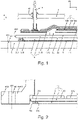
- figure 1 shows a side view of a first basic embodiment of a power semiconductor module according to the invention.
- This has a substrate 10, with a shaped insulation body 2 and arranged on its second main side 22, a first and a second conductor track 40,42.
- a power semiconductor component 44 is arranged on the second conductor track 42 of the substrate 10 and is electrically conductively connected thereto with its contact surface facing the second conductor track 42 .
- This electrically conductive connection is designed here, without loss of generality, as a pressure sintered connection that is integral with the material.
- the power semiconductor component 44 is connected to a first conductor track 40 by means of an internal connecting device 12.
- This connecting device 12 is designed as a foil composite made of a first electrically conductive foil 120 facing the substrate 10, an electrically insulating foil 122 following in the foil composite and a second electrically conductive foil 124 following in the foil composite.
- the power electronic device 1 also has a connection element 14, here more precisely an auxiliary connection element, for carrying auxiliary potentials, such as sensor or control signals, for example.
- This connection element 14 is designed as a press-fit contact element that is customary in the art.
- the foot of this press-fit contact element is arranged in an electrically conductive manner in a sleeve, with the sleeve being connected to a contact section on the surface of the first electrically conductive film 120 that is remote from the substrate 10 .
- the press-fit contact element extends through a recess 62 of a housing 6 of the power semiconductor module, which is only partially shown.
- This first electrically conductive film 120 is connected to the first conductor track 40 of the substrate 10 by means of a materially bonded and electrically conductive connection, designed here as a conventional pressure sintered connection.
- the substrate 10 also has a metallic layer 3 which is arranged on the first main side 20 of the molded insulation body 2 .
- the conductor tracks 40, 42 on the second main side 22 are formed from a further metallic layer by structuring it.
- the insulation molding 2 has a thickness of 300 ⁇ m here, while the metallic layers each have a thickness of 350 ⁇ m. These are typical values for such substrates 10 and also apply to the other exemplary embodiments.
- the metallic layer 3 is connected to a base plate 5 of the electronic power device 1 and thus to the power semiconductor module by means of a material connection 8 .
- This connection 8 has a thickness of approximately 150 ⁇ m and is designed here as a soldered connection.
- a likewise technically meaningful alternative to this is a sinter, in particular a pressure sinter, connection.
- the base plate 5 has a first fastening device 50 in the edge area or, more precisely here, in the corner area, which is designed here as a continuous cylindrical recess.
- the central axis 520 of this recess is also shown here. This recess is intended for the purpose of fastening the power semiconductor module to a cooling device, typically in a non-positive manner.
- the edge 300 of the metallic layer 3 is set back in relation to the edge 200 of the insulating molding 2 , as a result of which a peripheral edge section of the first main side 20 of the insulating molding 2 is not covered by the metallic layer 3 .
- Adjacent to the first fastening device 50, the edge of the metallic layer 300 is further set back in a first edge section 301 than in the respective adjoining second and third edge sections 302, 303, cf. Figures 3 to 10 . This results in an additional section of the first main side 20 of the insulating molding 2 that is not covered by the metallic layer 3 figure 9 described.
- figure 2 shows a side view of a second basic configuration of a power semiconductor module according to the invention.
- this has no base plate.
- the substrate 10 is intended to be arranged directly on a cooling device. In such configurations, it is typical, but not absolutely necessary, for the substrate 10 to be arranged in a non-positive manner on the cooling device.
- a housing 6 is arranged circumferentially around the substrate 10 and usually also covers the substrate, as is customary in the art.
- This housing has a second fastening device 60 in the edge or corner area, which in turn is designed as a continuous cylindrical recess.
- the central axis 620 of this recess is also shown here. This recess is intended for the purpose of fastening the power semiconductor module on the cooling device.
- the substrate 10 is configured here completely identically to that in the first embodiment according to FIG figure 1 .
- figure 3 shows a plane of a first embodiment of a power electronic device 1 according to the invention.
- a section through the metallic layer 3 is shown in a plan view from the normal direction N.
- the base plate 5 is arranged under this metallic layer 3 and has a first fastening device 50 with a diameter of 8mm on that, moreover, as below figure 1 described is formed.
- the metallic layer 3 has an edge 300 which is set back in relation to the edge 200 of the insulating molded body 2, which is partially shown in dashed lines.
- a first edge section 301 is formed adjacent to all of the first fastening devices 50 and is set back further in relation to the edge 200 of the insulating molded body 2 .
- This first section 301 is adjoined on the long side of the electronic power device 1 by a second edge section 302 of customary design and on the narrow side by a third edge section 303 that is also of customary design. These are therefore not set back as far as the first edge section 301.
- figure 4 shows a plane of a second embodiment of a power electronic device 1 according to the invention. Shown is a plan view of the substrate 10 from the normal direction N, wherein conductor tracks are not shown and the one power semiconductor device 44 shown is illustrative only. Below the molded insulation body 2, the metallic layer 3 is shown in a dotted manner. The base plate 5 is in turn arranged underneath, which here has a first fastening device 50 in the center on each of the narrow sides.
- the metallic layer 3 in turn has an edge 300 which is set back in relation to the edge 200 of the molded insulation body 2 .
- a first edge section 301 is formed adjacent to all of the first fastening devices 50 and is set back further in relation to the edge 200 of the insulating molded body 2 .
- this first section 301 which is located in the middle on the narrow side, is followed by a second and third edge section 302, 303 of customary design. These are therefore not set back as far as the first edge section 301.
- figure 5 shows a third embodiment of a power electronic device according to the invention with a plurality of substrates 10, three in this case by way of example.
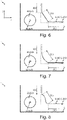
- Figures 6 to 10 show detailed illustrations of variants of the configuration of a power electronic device 1 according to the invention, in particular of the area in which the first edge section 301 is arranged.
- a corner of a base plate 5, comparable to Figure 3 or 5 shown.
- This corner area has a first fastening device 50, which is designed as a continuous cylindrical recess.
- Its virtual top surface 500 has a center point 52 through which the central axis 520, cf. figure 1 , vertically, in the z-direction.
- the molded insulation body 2 with its edge 200 and the metallic layer 3 on its first main side 20, cf. figure 1 .
- the respective embodiments differ in the design of the first edge section 301.
- the respective adjoining second and third edge sections 302, 303 are each designed the same as below Figure 3 and 5 described.
- the first edge section 301 according to the embodiment figure 6 is designed as a bevel of the corner area with a straight course.
- the first edge section 301 according to the embodiment figure 7 is designed with a convex course.
- the transition to the second edge section 302 is discontinuous, while that to the third edge section 303 is continuous.
- the first edge section 301 according to the embodiment figure 8 is designed as an example of a curve-like course with concave and convex, straight elements are also possible.
- the transition to the second edge section 302 is continuous, while that to the third edge section 303 is discontinuous.
- the first edge section 301 is designed with a concave profile, designed even more specifically here as a circle segment 321.
- the center point of the circle or of the circle segment 321 with a radius 311 lies here on the central axis 520, which extends centrally through the first fastening device 50.
- the center point of the circular segment 321 can lie anywhere within the top surface 500 of the first fastening device 50, which is designed as a cylindrical recess, in a projection onto the surface of the base plate 5.
- the center point 52 of the circle segment 321 can lie in the area 502 between the first fastening device 50 and the adjacent edge 504 of the base plate 5 in projection onto the surface of the base plate 5 .
- FIG 10 is a narrow side of a base plate 5, comparable to figure 4 , shown.
- a first fastening device 50 which in turn is designed as a continuous cylindrical recess, is arranged in the middle of this narrow side.
- the molded insulation body 2 with its edge 200 and the metallic layer on its first main side 20, cf. figure 1 .
- This first edge section 301 is followed by the second and third edge sections 302, 303, each of which has the same design as below figure 4 described.
- the first edge section 301 is in turn designed with a concave profile, here also designed again as a circle segment 321. With regard to the center point of the circle or of the circle segment 321, the following applies figure 9 already mentioned analogously.
Landscapes
- Cooling Or The Like Of Semiconductors Or Solid State Devices (AREA)
Priority Applications (3)
| Application Number | Priority Date | Filing Date | Title |
|---|---|---|---|
| EP20199403.5A EP3979313B1 (fr) | 2020-09-30 | 2020-09-30 | Dispositif électronique de puissance et module semi-conducteur de puissance correspondant |
| US17/481,986 US11967536B2 (en) | 2020-09-30 | 2021-09-22 | Electronic power unit and semiconductor power module |
| CN202111121226.3A CN114334892B (zh) | 2020-09-30 | 2021-09-24 | 电子功率单元和半导体功率模块 |
Applications Claiming Priority (1)
| Application Number | Priority Date | Filing Date | Title |
|---|---|---|---|
| EP20199403.5A EP3979313B1 (fr) | 2020-09-30 | 2020-09-30 | Dispositif électronique de puissance et module semi-conducteur de puissance correspondant |
Publications (2)
| Publication Number | Publication Date |
|---|---|
| EP3979313A1 true EP3979313A1 (fr) | 2022-04-06 |
| EP3979313B1 EP3979313B1 (fr) | 2022-11-30 |
Family
ID=72717665
Family Applications (1)
| Application Number | Title | Priority Date | Filing Date |
|---|---|---|---|
| EP20199403.5A Active EP3979313B1 (fr) | 2020-09-30 | 2020-09-30 | Dispositif électronique de puissance et module semi-conducteur de puissance correspondant |
Country Status (3)
| Country | Link |
|---|---|
| US (1) | US11967536B2 (fr) |
| EP (1) | EP3979313B1 (fr) |
| CN (1) | CN114334892B (fr) |
Families Citing this family (3)
| Publication number | Priority date | Publication date | Assignee | Title |
|---|---|---|---|---|
| JP7470074B2 (ja) * | 2021-03-10 | 2024-04-17 | 株式会社 日立パワーデバイス | 半導体モジュール |
| US12689140B2 (en) * | 2022-07-28 | 2026-07-21 | Infineon Technologies Ag | Press-fit connector and receptacle |
| EP4712138A1 (fr) * | 2024-09-17 | 2026-03-18 | Mitsubishi Electric R&D Centre Europe B.V. | Module semi-conducteur comprenant un support intermédiaire et un support principal |
Citations (6)
| Publication number | Priority date | Publication date | Assignee | Title |
|---|---|---|---|---|
| JP2000200865A (ja) * | 1999-01-06 | 2000-07-18 | Shibafu Engineering Kk | 絶縁基板及び半導体装置 |
| EP1217659A2 (fr) * | 2000-12-20 | 2002-06-26 | Semikron Elektronik GmbH | Module à semi-conducteur avec avec tension de claquage élevée |
| DE10063714A1 (de) | 2000-12-20 | 2002-07-04 | Semikron Elektronik Gmbh | Leistungshalbleitermodul mit hoher Isolationsfestigkeit |
| US20160020161A1 (en) * | 2014-07-15 | 2016-01-21 | Fuji Electric Co., Ltd. | Semiconductor device and semiconductor device manufacturing method |
| DE102015213495A1 (de) * | 2014-09-10 | 2016-03-10 | Mitsubishi Electric Corporation | Halbleitervorrichtung und Herstellungsverfahren dafür |
| EP3340291A1 (fr) * | 2016-12-23 | 2018-06-27 | Infineon Technologies AG | Procédé de production d'un ensemble de module électronique et ensemble de module électronique |
Family Cites Families (8)
| Publication number | Priority date | Publication date | Assignee | Title |
|---|---|---|---|---|
| DE102006040838B4 (de) * | 2006-08-31 | 2009-11-12 | DENSO CORPORATION, Kariya-shi | Elektronische Leistungspackung mit zwei Substraten mit mehreren Halbleiterchips und elektronischen Komponenten |
| DE102008034068B4 (de) * | 2008-07-22 | 2019-07-18 | Semikron Elektronik Gmbh & Co. Kg | Leistungshalbleitermodul |
| DE102012211952B4 (de) * | 2012-07-09 | 2019-04-25 | Semikron Elektronik Gmbh & Co. Kg | Leistungshalbleitermodul mit mindestens einem stressreduzierenden Anpasselement |
| DE102013104950B3 (de) * | 2013-05-14 | 2014-04-30 | Semikron Elektronik Gmbh & Co. Kg | Leistungshalbleitermodul und Anordnung hiermit |
| JP2015073012A (ja) * | 2013-10-03 | 2015-04-16 | 富士電機株式会社 | 半導体装置 |
| DE102015114191B3 (de) * | 2015-08-26 | 2016-11-03 | Semikron Elektronik Gmbh & Co. Kg | Leistungshalbleitermodul mit einer Mehrzahl von Submodulen und mit einer Druckeinrichtung und Anordnung hiermit |
| DE102017117667B4 (de) * | 2017-08-03 | 2021-11-18 | Semikron Elektronik Gmbh & Co. Kg | Leistungshalbleitermodul mit einer auf eine Schalteinrichtung einwirkenden Druckeinrichtung |
| US11145571B2 (en) * | 2019-06-04 | 2021-10-12 | Semiconductor Components Industries, Llc | Heat transfer for power modules |
-
2020
- 2020-09-30 EP EP20199403.5A patent/EP3979313B1/fr active Active
-
2021
- 2021-09-22 US US17/481,986 patent/US11967536B2/en active Active
- 2021-09-24 CN CN202111121226.3A patent/CN114334892B/zh active Active
Patent Citations (6)
| Publication number | Priority date | Publication date | Assignee | Title |
|---|---|---|---|---|
| JP2000200865A (ja) * | 1999-01-06 | 2000-07-18 | Shibafu Engineering Kk | 絶縁基板及び半導体装置 |
| EP1217659A2 (fr) * | 2000-12-20 | 2002-06-26 | Semikron Elektronik GmbH | Module à semi-conducteur avec avec tension de claquage élevée |
| DE10063714A1 (de) | 2000-12-20 | 2002-07-04 | Semikron Elektronik Gmbh | Leistungshalbleitermodul mit hoher Isolationsfestigkeit |
| US20160020161A1 (en) * | 2014-07-15 | 2016-01-21 | Fuji Electric Co., Ltd. | Semiconductor device and semiconductor device manufacturing method |
| DE102015213495A1 (de) * | 2014-09-10 | 2016-03-10 | Mitsubishi Electric Corporation | Halbleitervorrichtung und Herstellungsverfahren dafür |
| EP3340291A1 (fr) * | 2016-12-23 | 2018-06-27 | Infineon Technologies AG | Procédé de production d'un ensemble de module électronique et ensemble de module électronique |
Also Published As
| Publication number | Publication date |
|---|---|
| US20220102227A1 (en) | 2022-03-31 |
| CN114334892B (zh) | 2025-06-13 |
| CN114334892A (zh) | 2022-04-12 |
| EP3979313B1 (fr) | 2022-11-30 |
| US11967536B2 (en) | 2024-04-23 |
Similar Documents
| Publication | Publication Date | Title |
|---|---|---|
| DE102008017454B4 (de) | Leistungshalbleitermodul mit hermetisch dichter Schaltungsanordnung und Herstellungsverfahren hierzu | |
| DE102017115883B4 (de) | Leistungselektronisches Submodul mit Gleich- und Wechselspannungsanschlusselementen und Anordnung hiermit | |
| EP3262666B1 (fr) | Composant électrique et procédé de manufacture de ce composant | |
| DE4318241C2 (de) | Metallbeschichtetes Substrat mit verbesserter Widerstandsfähigkeit gegen Temperaturwechselbeanspruchung | |
| DE102017109706B3 (de) | Leistungselektronische Anordnung mit Gleichspannungsverbindungselement | |
| EP3979313B1 (fr) | Dispositif électronique de puissance et module semi-conducteur de puissance correspondant | |
| DE102013100701B4 (de) | Halbleitermodulanordnung und verfahren zur herstellung einer halbleitermodulanordnung | |
| EP3138161B1 (fr) | Élément de contact pour connexion électrique et feuillard de cuivre servant à fabriquer une pluralité d'éléments de contact | |
| DE102018204473B4 (de) | Halbleitervorrichtung | |
| EP1631988B1 (fr) | Module semi-conducteur de puissance | |
| DE102019117476B4 (de) | Leistungselektronische Schalteinrichtung mit einem Anschlusselement | |
| EP1772902B1 (fr) | Module semiconducteur de puissance avec couche isolante intermédiaire et méthode de fabrication | |
| EP4086954B1 (fr) | Ensemble semi-conducteur de puissance comprenant élément de contact à presser doté d'une section de compensation et d'une section de blocage | |
| DE102020122784A1 (de) | Leistungselektronische Schalteinrichtung mit einem dreidimensional vorgeformten Isolationsformkörper und Verfahren zu deren Herstellung | |
| EP1791178A2 (fr) | Module de puissance semi-conducteur de type à contact par pression | |
| DE102017107763B4 (de) | Leistungshalbleitereinrichtung, Leistungshalbleiteranordnung und Verfahren zur Herstellung einer Leistungshalbleiteranordnung | |
| DE102019118421A1 (de) | Leistungselektronische Schalteinrichtung mit einem Verbindungsmittel und mit einem Leistungshalbleiterbauelement | |
| DE102020119141B4 (de) | Leistungselektronische Schalteinrichtung mit einem Anschlusselement und einer Verbindungseinrichtung | |
| EP2148368B1 (fr) | Module semi-conducteur de puissance | |
| DE102017122557A1 (de) | Leitungselektronische Anordnung mit einem Folienverbund und mit einem Verbindungspartner | |
| DE102016115373B4 (de) | Schaltungsanordnung mit einer Verbindungseinrichtung und mit einer Leiterplatte | |
| EP3740050A1 (fr) | Carte de circuit imprimé dotée d'un connecteur enfichable | |
| DE102009050178B3 (de) | Leistungshalbleitermodul mit einem eine dreidimensionale Oberflächenkontur aufweisenden Substrat sowie Herstellungsverfahren hierzu | |
| DE202024103126U1 (de) | Leistungselektronische Schalteinrichtung mit einem Ausgleichskörper | |
| DE102022133512A1 (de) | Leistungshalbleitermodul mit einem Gehäuse, einer leistungselektronischen Baugruppe und mit einem Formkörper |
Legal Events
| Date | Code | Title | Description |
|---|---|---|---|
| PUAI | Public reference made under article 153(3) epc to a published international application that has entered the european phase |
Free format text: ORIGINAL CODE: 0009012 |
|
| STAA | Information on the status of an ep patent application or granted ep patent |
Free format text: STATUS: REQUEST FOR EXAMINATION WAS MADE |
|
| 17P | Request for examination filed |
Effective date: 20210426 |
|
| AK | Designated contracting states |
Kind code of ref document: A1 Designated state(s): AL AT BE BG CH CY CZ DE DK EE ES FI FR GB GR HR HU IE IS IT LI LT LU LV MC MK MT NL NO PL PT RO RS SE SI SK SM TR |
|
| RBV | Designated contracting states (corrected) |
Designated state(s): AL AT BE BG CH CY CZ DE DK EE ES FI FR GB GR HR HU IE IS IT LI LT LU LV MC MK MT NL NO PL PT RO RS SE SI SK SM TR |
|
| GRAP | Despatch of communication of intention to grant a patent |
Free format text: ORIGINAL CODE: EPIDOSNIGR1 |
|
| STAA | Information on the status of an ep patent application or granted ep patent |
Free format text: STATUS: GRANT OF PATENT IS INTENDED |
|
| RIC1 | Information provided on ipc code assigned before grant |
Ipc: H01L 23/40 20060101ALI20220706BHEP Ipc: H01L 23/373 20060101AFI20220706BHEP |
|
| INTG | Intention to grant announced |
Effective date: 20220720 |
|
| GRAS | Grant fee paid |
Free format text: ORIGINAL CODE: EPIDOSNIGR3 |
|
| GRAA | (expected) grant |
Free format text: ORIGINAL CODE: 0009210 |
|
| STAA | Information on the status of an ep patent application or granted ep patent |
Free format text: STATUS: THE PATENT HAS BEEN GRANTED |
|
| AK | Designated contracting states |
Kind code of ref document: B1 Designated state(s): AL AT BE BG CH CY CZ DE DK EE ES FI FR GB GR HR HU IE IS IT LI LT LU LV MC MK MT NL NO PL PT RO RS SE SI SK SM TR |
|
| REG | Reference to a national code |
Ref country code: CH Ref legal event code: EP Ref country code: GB Ref legal event code: FG4D Free format text: NOT ENGLISH |
|
| REG | Reference to a national code |
Ref country code: AT Ref legal event code: REF Ref document number: 1535333 Country of ref document: AT Kind code of ref document: T Effective date: 20221215 |
|
| REG | Reference to a national code |
Ref country code: IE Ref legal event code: FG4D Free format text: LANGUAGE OF EP DOCUMENT: GERMAN |
|
| REG | Reference to a national code |
Ref country code: DE Ref legal event code: R096 Ref document number: 502020002095 Country of ref document: DE |
|
| REG | Reference to a national code |
Ref country code: LT Ref legal event code: MG9D |
|
| REG | Reference to a national code |
Ref country code: NL Ref legal event code: MP Effective date: 20221130 |
|
| PG25 | Lapsed in a contracting state [announced via postgrant information from national office to epo] |
Ref country code: SE Free format text: LAPSE BECAUSE OF FAILURE TO SUBMIT A TRANSLATION OF THE DESCRIPTION OR TO PAY THE FEE WITHIN THE PRESCRIBED TIME-LIMIT Effective date: 20221130 Ref country code: PT Free format text: LAPSE BECAUSE OF FAILURE TO SUBMIT A TRANSLATION OF THE DESCRIPTION OR TO PAY THE FEE WITHIN THE PRESCRIBED TIME-LIMIT Effective date: 20230331 Ref country code: NO Free format text: LAPSE BECAUSE OF FAILURE TO SUBMIT A TRANSLATION OF THE DESCRIPTION OR TO PAY THE FEE WITHIN THE PRESCRIBED TIME-LIMIT Effective date: 20230228 Ref country code: LT Free format text: LAPSE BECAUSE OF FAILURE TO SUBMIT A TRANSLATION OF THE DESCRIPTION OR TO PAY THE FEE WITHIN THE PRESCRIBED TIME-LIMIT Effective date: 20221130 Ref country code: FI Free format text: LAPSE BECAUSE OF FAILURE TO SUBMIT A TRANSLATION OF THE DESCRIPTION OR TO PAY THE FEE WITHIN THE PRESCRIBED TIME-LIMIT Effective date: 20221130 Ref country code: ES Free format text: LAPSE BECAUSE OF FAILURE TO SUBMIT A TRANSLATION OF THE DESCRIPTION OR TO PAY THE FEE WITHIN THE PRESCRIBED TIME-LIMIT Effective date: 20221130 |
|
| PG25 | Lapsed in a contracting state [announced via postgrant information from national office to epo] |
Ref country code: RS Free format text: LAPSE BECAUSE OF FAILURE TO SUBMIT A TRANSLATION OF THE DESCRIPTION OR TO PAY THE FEE WITHIN THE PRESCRIBED TIME-LIMIT Effective date: 20221130 Ref country code: PL Free format text: LAPSE BECAUSE OF FAILURE TO SUBMIT A TRANSLATION OF THE DESCRIPTION OR TO PAY THE FEE WITHIN THE PRESCRIBED TIME-LIMIT Effective date: 20221130 Ref country code: LV Free format text: LAPSE BECAUSE OF FAILURE TO SUBMIT A TRANSLATION OF THE DESCRIPTION OR TO PAY THE FEE WITHIN THE PRESCRIBED TIME-LIMIT Effective date: 20221130 Ref country code: IS Free format text: LAPSE BECAUSE OF FAILURE TO SUBMIT A TRANSLATION OF THE DESCRIPTION OR TO PAY THE FEE WITHIN THE PRESCRIBED TIME-LIMIT Effective date: 20230330 Ref country code: HR Free format text: LAPSE BECAUSE OF FAILURE TO SUBMIT A TRANSLATION OF THE DESCRIPTION OR TO PAY THE FEE WITHIN THE PRESCRIBED TIME-LIMIT Effective date: 20221130 Ref country code: GR Free format text: LAPSE BECAUSE OF FAILURE TO SUBMIT A TRANSLATION OF THE DESCRIPTION OR TO PAY THE FEE WITHIN THE PRESCRIBED TIME-LIMIT Effective date: 20230301 |
|
| PG25 | Lapsed in a contracting state [announced via postgrant information from national office to epo] |
Ref country code: NL Free format text: LAPSE BECAUSE OF FAILURE TO SUBMIT A TRANSLATION OF THE DESCRIPTION OR TO PAY THE FEE WITHIN THE PRESCRIBED TIME-LIMIT Effective date: 20221130 |
|
| PG25 | Lapsed in a contracting state [announced via postgrant information from national office to epo] |
Ref country code: SM Free format text: LAPSE BECAUSE OF FAILURE TO SUBMIT A TRANSLATION OF THE DESCRIPTION OR TO PAY THE FEE WITHIN THE PRESCRIBED TIME-LIMIT Effective date: 20221130 Ref country code: RO Free format text: LAPSE BECAUSE OF FAILURE TO SUBMIT A TRANSLATION OF THE DESCRIPTION OR TO PAY THE FEE WITHIN THE PRESCRIBED TIME-LIMIT Effective date: 20221130 Ref country code: EE Free format text: LAPSE BECAUSE OF FAILURE TO SUBMIT A TRANSLATION OF THE DESCRIPTION OR TO PAY THE FEE WITHIN THE PRESCRIBED TIME-LIMIT Effective date: 20221130 Ref country code: DK Free format text: LAPSE BECAUSE OF FAILURE TO SUBMIT A TRANSLATION OF THE DESCRIPTION OR TO PAY THE FEE WITHIN THE PRESCRIBED TIME-LIMIT Effective date: 20221130 Ref country code: CZ Free format text: LAPSE BECAUSE OF FAILURE TO SUBMIT A TRANSLATION OF THE DESCRIPTION OR TO PAY THE FEE WITHIN THE PRESCRIBED TIME-LIMIT Effective date: 20221130 |
|
| PG25 | Lapsed in a contracting state [announced via postgrant information from national office to epo] |
Ref country code: SK Free format text: LAPSE BECAUSE OF FAILURE TO SUBMIT A TRANSLATION OF THE DESCRIPTION OR TO PAY THE FEE WITHIN THE PRESCRIBED TIME-LIMIT Effective date: 20221130 Ref country code: AL Free format text: LAPSE BECAUSE OF FAILURE TO SUBMIT A TRANSLATION OF THE DESCRIPTION OR TO PAY THE FEE WITHIN THE PRESCRIBED TIME-LIMIT Effective date: 20221130 |
|
| REG | Reference to a national code |
Ref country code: DE Ref legal event code: R097 Ref document number: 502020002095 Country of ref document: DE |
|
| PLBE | No opposition filed within time limit |
Free format text: ORIGINAL CODE: 0009261 |
|
| STAA | Information on the status of an ep patent application or granted ep patent |
Free format text: STATUS: NO OPPOSITION FILED WITHIN TIME LIMIT |
|
| 26N | No opposition filed |
Effective date: 20230831 |
|
| PG25 | Lapsed in a contracting state [announced via postgrant information from national office to epo] |
Ref country code: SI Free format text: LAPSE BECAUSE OF FAILURE TO SUBMIT A TRANSLATION OF THE DESCRIPTION OR TO PAY THE FEE WITHIN THE PRESCRIBED TIME-LIMIT Effective date: 20221130 |
|
| REG | Reference to a national code |
Ref country code: CH Ref legal event code: PL |
|
| PG25 | Lapsed in a contracting state [announced via postgrant information from national office to epo] |
Ref country code: LU Free format text: LAPSE BECAUSE OF NON-PAYMENT OF DUE FEES Effective date: 20230930 |
|
| REG | Reference to a national code |
Ref country code: BE Ref legal event code: MM Effective date: 20230930 |
|
| PG25 | Lapsed in a contracting state [announced via postgrant information from national office to epo] |
Ref country code: LU Free format text: LAPSE BECAUSE OF NON-PAYMENT OF DUE FEES Effective date: 20230930 Ref country code: MC Free format text: LAPSE BECAUSE OF FAILURE TO SUBMIT A TRANSLATION OF THE DESCRIPTION OR TO PAY THE FEE WITHIN THE PRESCRIBED TIME-LIMIT Effective date: 20221130 |
|
| REG | Reference to a national code |
Ref country code: IE Ref legal event code: MM4A |
|
| PG25 | Lapsed in a contracting state [announced via postgrant information from national office to epo] |
Ref country code: IE Free format text: LAPSE BECAUSE OF NON-PAYMENT OF DUE FEES Effective date: 20230930 |
|
| PG25 | Lapsed in a contracting state [announced via postgrant information from national office to epo] |
Ref country code: CH Free format text: LAPSE BECAUSE OF NON-PAYMENT OF DUE FEES Effective date: 20230930 |
|
| PG25 | Lapsed in a contracting state [announced via postgrant information from national office to epo] |
Ref country code: IE Free format text: LAPSE BECAUSE OF NON-PAYMENT OF DUE FEES Effective date: 20230930 Ref country code: FR Free format text: LAPSE BECAUSE OF NON-PAYMENT OF DUE FEES Effective date: 20230930 Ref country code: CH Free format text: LAPSE BECAUSE OF NON-PAYMENT OF DUE FEES Effective date: 20230930 |
|
| PG25 | Lapsed in a contracting state [announced via postgrant information from national office to epo] |
Ref country code: BE Free format text: LAPSE BECAUSE OF NON-PAYMENT OF DUE FEES Effective date: 20230930 |
|
| PG25 | Lapsed in a contracting state [announced via postgrant information from national office to epo] |
Ref country code: BG Free format text: LAPSE BECAUSE OF FAILURE TO SUBMIT A TRANSLATION OF THE DESCRIPTION OR TO PAY THE FEE WITHIN THE PRESCRIBED TIME-LIMIT Effective date: 20221130 |
|
| PG25 | Lapsed in a contracting state [announced via postgrant information from national office to epo] |
Ref country code: BG Free format text: LAPSE BECAUSE OF FAILURE TO SUBMIT A TRANSLATION OF THE DESCRIPTION OR TO PAY THE FEE WITHIN THE PRESCRIBED TIME-LIMIT Effective date: 20221130 |
|
| GBPC | Gb: european patent ceased through non-payment of renewal fee |
Effective date: 20240930 |
|
| PG25 | Lapsed in a contracting state [announced via postgrant information from national office to epo] |
Ref country code: GB Free format text: LAPSE BECAUSE OF NON-PAYMENT OF DUE FEES Effective date: 20240930 |
|
| PG25 | Lapsed in a contracting state [announced via postgrant information from national office to epo] |
Ref country code: CY Free format text: LAPSE BECAUSE OF FAILURE TO SUBMIT A TRANSLATION OF THE DESCRIPTION OR TO PAY THE FEE WITHIN THE PRESCRIBED TIME-LIMIT; INVALID AB INITIO Effective date: 20200930 |
|
| PG25 | Lapsed in a contracting state [announced via postgrant information from national office to epo] |
Ref country code: HU Free format text: LAPSE BECAUSE OF FAILURE TO SUBMIT A TRANSLATION OF THE DESCRIPTION OR TO PAY THE FEE WITHIN THE PRESCRIBED TIME-LIMIT; INVALID AB INITIO Effective date: 20200930 |
|
| PGFP | Annual fee paid to national office [announced via postgrant information from national office to epo] |
Ref country code: DE Payment date: 20250805 Year of fee payment: 6 |
|
| REG | Reference to a national code |
Ref country code: DE Ref legal event code: R081 Ref document number: 502020002095 Country of ref document: DE Owner name: SEMIKRON DANFOSS ELEKTRONIK GMBH & CO. KG, DE Free format text: FORMER OWNER: SEMIKRON ELEKTRONIK GMBH & CO. KG, 90431 NUERNBERG, DE |
|
| PGFP | Annual fee paid to national office [announced via postgrant information from national office to epo] |
Ref country code: IT Payment date: 20250825 Year of fee payment: 6 |
|
| PGFP | Annual fee paid to national office [announced via postgrant information from national office to epo] |
Ref country code: AT Payment date: 20251020 Year of fee payment: 5 |
|
| REG | Reference to a national code |
Ref country code: DE Ref legal event code: R079 Ref document number: 502020002095 Country of ref document: DE Free format text: PREVIOUS MAIN CLASS: H01L0023373000 Ipc: H10W0040250000 |
|
| PG25 | Lapsed in a contracting state [announced via postgrant information from national office to epo] |
Ref country code: TR Free format text: LAPSE BECAUSE OF FAILURE TO SUBMIT A TRANSLATION OF THE DESCRIPTION OR TO PAY THE FEE WITHIN THE PRESCRIBED TIME-LIMIT Effective date: 20221130 |