EP3985143A1 - Plateau composite - Google Patents
Plateau composite Download PDFInfo
- Publication number
- EP3985143A1 EP3985143A1 EP20836223.6A EP20836223A EP3985143A1 EP 3985143 A1 EP3985143 A1 EP 3985143A1 EP 20836223 A EP20836223 A EP 20836223A EP 3985143 A1 EP3985143 A1 EP 3985143A1
- Authority
- EP
- European Patent Office
- Prior art keywords
- base
- composite tray
- supporting components
- tray according
- supporting
- Prior art date
- Legal status (The legal status is an assumption and is not a legal conclusion. Google has not performed a legal analysis and makes no representation as to the accuracy of the status listed.)
- Pending
Links
Images



Classifications
-
- C—CHEMISTRY; METALLURGY
- C23—COATING METALLIC MATERIAL; COATING MATERIAL WITH METALLIC MATERIAL; CHEMICAL SURFACE TREATMENT; DIFFUSION TREATMENT OF METALLIC MATERIAL; COATING BY VACUUM EVAPORATION, BY SPUTTERING, BY ION IMPLANTATION OR BY CHEMICAL VAPOUR DEPOSITION, IN GENERAL; INHIBITING CORROSION OF METALLIC MATERIAL OR INCRUSTATION IN GENERAL
- C23C—COATING METALLIC MATERIAL; COATING MATERIAL WITH METALLIC MATERIAL; SURFACE TREATMENT OF METALLIC MATERIAL BY DIFFUSION INTO THE SURFACE, BY CHEMICAL CONVERSION OR SUBSTITUTION; COATING BY VACUUM EVAPORATION, BY SPUTTERING, BY ION IMPLANTATION OR BY CHEMICAL VAPOUR DEPOSITION, IN GENERAL
- C23C16/00—Chemical coating by decomposition of gaseous compounds, without leaving reaction products of surface material in the coating, i.e. chemical vapour deposition [CVD] processes
- C23C16/44—Chemical coating by decomposition of gaseous compounds, without leaving reaction products of surface material in the coating, i.e. chemical vapour deposition [CVD] processes characterised by the method of coating
- C23C16/458—Chemical coating by decomposition of gaseous compounds, without leaving reaction products of surface material in the coating, i.e. chemical vapour deposition [CVD] processes characterised by the method of coating characterised by the method used for supporting substrates in the reaction chamber
- C23C16/4581—Chemical coating by decomposition of gaseous compounds, without leaving reaction products of surface material in the coating, i.e. chemical vapour deposition [CVD] processes characterised by the method of coating characterised by the method used for supporting substrates in the reaction chamber characterised by material of construction or surface finish of the means for supporting the substrate
-
- C—CHEMISTRY; METALLURGY
- C23—COATING METALLIC MATERIAL; COATING MATERIAL WITH METALLIC MATERIAL; CHEMICAL SURFACE TREATMENT; DIFFUSION TREATMENT OF METALLIC MATERIAL; COATING BY VACUUM EVAPORATION, BY SPUTTERING, BY ION IMPLANTATION OR BY CHEMICAL VAPOUR DEPOSITION, IN GENERAL; INHIBITING CORROSION OF METALLIC MATERIAL OR INCRUSTATION IN GENERAL
- C23C—COATING METALLIC MATERIAL; COATING MATERIAL WITH METALLIC MATERIAL; SURFACE TREATMENT OF METALLIC MATERIAL BY DIFFUSION INTO THE SURFACE, BY CHEMICAL CONVERSION OR SUBSTITUTION; COATING BY VACUUM EVAPORATION, BY SPUTTERING, BY ION IMPLANTATION OR BY CHEMICAL VAPOUR DEPOSITION, IN GENERAL
- C23C16/00—Chemical coating by decomposition of gaseous compounds, without leaving reaction products of surface material in the coating, i.e. chemical vapour deposition [CVD] processes
- C23C16/44—Chemical coating by decomposition of gaseous compounds, without leaving reaction products of surface material in the coating, i.e. chemical vapour deposition [CVD] processes characterised by the method of coating
- C23C16/458—Chemical coating by decomposition of gaseous compounds, without leaving reaction products of surface material in the coating, i.e. chemical vapour deposition [CVD] processes characterised by the method of coating characterised by the method used for supporting substrates in the reaction chamber
-
- C—CHEMISTRY; METALLURGY
- C23—COATING METALLIC MATERIAL; COATING MATERIAL WITH METALLIC MATERIAL; CHEMICAL SURFACE TREATMENT; DIFFUSION TREATMENT OF METALLIC MATERIAL; COATING BY VACUUM EVAPORATION, BY SPUTTERING, BY ION IMPLANTATION OR BY CHEMICAL VAPOUR DEPOSITION, IN GENERAL; INHIBITING CORROSION OF METALLIC MATERIAL OR INCRUSTATION IN GENERAL
- C23C—COATING METALLIC MATERIAL; COATING MATERIAL WITH METALLIC MATERIAL; SURFACE TREATMENT OF METALLIC MATERIAL BY DIFFUSION INTO THE SURFACE, BY CHEMICAL CONVERSION OR SUBSTITUTION; COATING BY VACUUM EVAPORATION, BY SPUTTERING, BY ION IMPLANTATION OR BY CHEMICAL VAPOUR DEPOSITION, IN GENERAL
- C23C16/00—Chemical coating by decomposition of gaseous compounds, without leaving reaction products of surface material in the coating, i.e. chemical vapour deposition [CVD] processes
- C23C16/44—Chemical coating by decomposition of gaseous compounds, without leaving reaction products of surface material in the coating, i.e. chemical vapour deposition [CVD] processes characterised by the method of coating
- C23C16/458—Chemical coating by decomposition of gaseous compounds, without leaving reaction products of surface material in the coating, i.e. chemical vapour deposition [CVD] processes characterised by the method of coating characterised by the method used for supporting substrates in the reaction chamber
- C23C16/4582—Rigid and flat substrates, e.g. plates or discs
- C23C16/4583—Rigid and flat substrates, e.g. plates or discs the substrate being supported substantially horizontally
- C23C16/4585—Devices at or outside the perimeter of the substrate support, e.g. clamping rings, shrouds
-
- H—ELECTRICITY
- H10—SEMICONDUCTOR DEVICES; ELECTRIC SOLID-STATE DEVICES NOT OTHERWISE PROVIDED FOR
- H10P—GENERIC PROCESSES OR APPARATUS FOR THE MANUFACTURE OR TREATMENT OF DEVICES COVERED BY CLASS H10
- H10P72/00—Handling or holding of wafers, substrates or devices during manufacture or treatment thereof
- H10P72/10—Handling or holding of wafers, substrates or devices during manufacture or treatment thereof using carriers specially adapted therefor, e.g. front opening unified pods [FOUP]
- H10P72/17—Handling or holding of wafers, substrates or devices during manufacture or treatment thereof using carriers specially adapted therefor, e.g. front opening unified pods [FOUP] specially adapted for supporting large square shaped substrates
-
- H—ELECTRICITY
- H10—SEMICONDUCTOR DEVICES; ELECTRIC SOLID-STATE DEVICES NOT OTHERWISE PROVIDED FOR
- H10P—GENERIC PROCESSES OR APPARATUS FOR THE MANUFACTURE OR TREATMENT OF DEVICES COVERED BY CLASS H10
- H10P72/00—Handling or holding of wafers, substrates or devices during manufacture or treatment thereof
- H10P72/10—Handling or holding of wafers, substrates or devices during manufacture or treatment thereof using carriers specially adapted therefor, e.g. front opening unified pods [FOUP]
- H10P72/17—Handling or holding of wafers, substrates or devices during manufacture or treatment thereof using carriers specially adapted therefor, e.g. front opening unified pods [FOUP] specially adapted for supporting large square shaped substrates
- H10P72/175—Handling or holding of wafers, substrates or devices during manufacture or treatment thereof using carriers specially adapted therefor, e.g. front opening unified pods [FOUP] specially adapted for supporting large square shaped substrates characterised by a material, a roughness, a coating or the like
-
- H—ELECTRICITY
- H10—SEMICONDUCTOR DEVICES; ELECTRIC SOLID-STATE DEVICES NOT OTHERWISE PROVIDED FOR
- H10P—GENERIC PROCESSES OR APPARATUS FOR THE MANUFACTURE OR TREATMENT OF DEVICES COVERED BY CLASS H10
- H10P72/00—Handling or holding of wafers, substrates or devices during manufacture or treatment thereof
- H10P72/70—Handling or holding of wafers, substrates or devices during manufacture or treatment thereof for supporting or gripping
- H10P72/76—Handling or holding of wafers, substrates or devices during manufacture or treatment thereof for supporting or gripping using mechanical means, e.g. clamps or pinches
- H10P72/7604—Handling or holding of wafers, substrates or devices during manufacture or treatment thereof for supporting or gripping using mechanical means, e.g. clamps or pinches the wafers being placed on a susceptor, stage or support
- H10P72/7616—Handling or holding of wafers, substrates or devices during manufacture or treatment thereof for supporting or gripping using mechanical means, e.g. clamps or pinches the wafers being placed on a susceptor, stage or support characterised by a coating, a hardness or a material
-
- H—ELECTRICITY
- H10—SEMICONDUCTOR DEVICES; ELECTRIC SOLID-STATE DEVICES NOT OTHERWISE PROVIDED FOR
- H10P—GENERIC PROCESSES OR APPARATUS FOR THE MANUFACTURE OR TREATMENT OF DEVICES COVERED BY CLASS H10
- H10P72/00—Handling or holding of wafers, substrates or devices during manufacture or treatment thereof
- H10P72/70—Handling or holding of wafers, substrates or devices during manufacture or treatment thereof for supporting or gripping
- H10P72/76—Handling or holding of wafers, substrates or devices during manufacture or treatment thereof for supporting or gripping using mechanical means, e.g. clamps or pinches
- H10P72/7604—Handling or holding of wafers, substrates or devices during manufacture or treatment thereof for supporting or gripping using mechanical means, e.g. clamps or pinches the wafers being placed on a susceptor, stage or support
- H10P72/7621—Handling or holding of wafers, substrates or devices during manufacture or treatment thereof for supporting or gripping using mechanical means, e.g. clamps or pinches the wafers being placed on a susceptor, stage or support characterised by supporting two or more semiconductor substrates
Definitions
- the present application relates to the field of cell manufacturing technology, and more particularly relates to a composite tray.
- a composite tray in a silicon wafer coating equipment is an important process device for bearing silicon wafers in PECVD (Plasma Enhanced Chemical Vapor Deposition).
- the composite tray in the prior art is generally made of one material, for example, the composite tray is made of a C/C (carbon/carbon) composite material.
- the C/C composite material is a novel high-performance structural and functional composite material and has excellent characteristics of high strength, high modulus, high fracture toughness, high heat conduction, excellent heat insulation, low density, and the like.
- due to the high price of the composite tray made of the C/C composite material requiring the number of the composite trays made of C/C composite materials to be multiple will inevitably increase investment, increase costs and maintenance costs.
- the composite tray made of the C/C composite material also absorbs water and moisture, which affects the coating process.
- the composite tray may be made of aluminum alloy material, but the single aluminum alloy material deforms greatly and conducts heat too quickly.
- the composite tray may be made of graphite material, and the single graphite material has no burrs and less water absorption, but has insufficient strength.
- the purpose of the present application is to provide an improved composite tray in view of the problems in the prior art.
- a composite tray includes supporting components and a base configured for receiving the supporting components.
- Each of the supporting components is provided with a silicon wafer receiving area configured for receiving a silicon wafer, and the base and the supporting components are made of different materials.
- the base is made of C/C composite material
- the supporting component is made of graphite material.
- the base is provided with a groove configured for receiving the supporting component, and the groove extends through one end surface of the base.
- the base is provided with openings configured for receiving the supporting component, and the openings extend through opposite two end surfaces of the base.
- the supporting component is detachably connected to the base.
- the composite tray further includes a connecting element configured to connect the base with the supporting component, and the connecting element is a bolt, a hook, a buckle, or a sheet metal pressing strip.
- the base is connected to the supporting component by transition fit.
- the plurality of supporting components are arranged independently from each other.
- the two adjacent supporting components have overlapping areas that overlap with each other.
- the two adjacent supporting components are connected through a set of connecting elements, and the connecting elements are disposed at positions of the overlapping areas.
- each of the supporting components is integrally formed with at least one adjacent supporting component to form a connected-piece structure.
- the two adjacent supporting components have overlapping areas that overlap with each other.
- the two adjacent supporting components are connected through a set of connecting elements, and the connecting elements are disposed at positions of the overlapping areas.
- the plurality of supporting components are arranged on the base in a matrix form.
- the supporting components have a plurality of specifications, and the supporting components of the plurality of specifications are replaceably arranged on the base.
- the silicon wafer receiving area of the supporting component is provided with cutting grooves on four corners thereof.
- the silicon wafer receiving area of the supporting component is provided with chamfers or fillets on four corners thereof.
- the supporting components of the plurality of specifications have different sizes of the silicon wafer receiving areas.
- the present application has the following advantages compared with the prior art: the composite tray according to the present application is made of two different materials, and thus can overcome the defects of the composite tray made of a single material, which can not only meet the performances of strength, heat insulation, heat conduction, and the like, but also has relatively low cost and is beneficial to batch use.
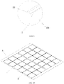
- a composite tray includes a base 1 and a supporting component 2 disposed on the base 1.
- the base 1 and the supporting component 2 are made of different materials.
- the base 1 is made of a C/C composite material
- the supporting component 2 is made of a graphite material, so that the composite tray not only has the excellent characteristics of high strength, high modulus, high fracture toughness, high heat conduction, excellent heat insulation, low density, and the like of the C/C composite material, but also has the characteristics of low cost, low water absorption, and no burrs of the graphite material.
- the production cost of the composite tray is low, and during the silicon wafer coating process, the performance of the composite tray has the least influence on a silicon wafer coating process.
- the base 1 is provided with a plurality of receiving portions, preferably, the plurality of receiving portions are arranged in a matrix form, each of which is provided with one supporting component 2 therein.
- the receiving portion may be a groove provided on the base 1, where the groove only extends through one end surface of the base 1.
- the receiving portion may also be an opening provided on the base 1, and the opening extends through the opposite two end surfaces of the base 1.
- the supporting component 2 is further provided with a silicon wafer receiving area for receiving the silicon wafer 100. When the silicon wafer 100 is coated, the supporting component 2 is mounted in the receiving portion on the base 1, and the silicon wafer 100 is placed in the silicon wafer receiving area on the supporting component 2.
- the base 1 and the supporting component 2 are detachably connected such that the supporting component 2 can be replaced.
- the supporting component 2 has a variety of specifications, the structures of the parts, connected with the base 1, of the supporting components 2 of various specifications are kept consistent.
- the structures and the sizes of the silicon wafer receiving areas of the supporting components 2 of various specifications are determined according to different sizes or different structures of the silicon wafers 100, as long as the silicon wafer receiving areas are matched with the silicon wafers 100 required to be placed.
- the silicon wafer receiving area of the supporting component 2 is provided with cutting grooves 21 on four corners thereof to prevent right angle corners of the silicon wafer 100 from being damaged, as shown in FIGS. 6 and 7 .
- the silicon wafer receiving area of the supporting component 2 is provided with chamfers 22 or fillets 22 on the four corners thereof, as shown in FIGS. 8 and 9 .
- the sizes of the silicon wafer receiving areas of the supporting components 2 of various specifications are different.
- the composite tray further includes a connecting element 3 for connecting the base 1 and the supporting component 2.
- the connecting element 3 can be a bolt, a hook, a buckle, or a sheet metal pressing strip, as shown in FIGS. 10 and 11 .
- the base 1 and the supporting component 2 can also be connected by transition fit, so that the connecting element 3 does not need to be provided.
- the supporting components 2 can be arranged independently from each other, i.e., the supporting components 2 are of a one-piece structure. It is also possible that each supporting component 2 is integrally formed with at least one adjacent supporting component 2 to form a connected-piece structure.
- the base 1 is provided with 36 receiving portions, that is, the composite tray includes 36 supporting components.
- the 36 supporting components 2 and the 36 receiving portions are all arranged in a 6 ⁇ 6 matrix form.
- the supporting components 2 can form a connected-piece structure such as 1 ⁇ 2, 1 ⁇ 3, 1 ⁇ 4, 1 ⁇ 5..., 2 ⁇ 3, 2 ⁇ 4, 2 ⁇ 5..., 3 ⁇ 3, 3 ⁇ 4, 3 ⁇ 5, 3 ⁇ 6..., 4 ⁇ 4, 4 ⁇ 5, 4 ⁇ 6... ..., and the like.
- the supporting component 2 adopts a connected-piece structure
- the number of the connecting structures between the supporting component 2 and the base 1 can be reduced, thereby facilitating the mounting and the disassembly of the supporting component 2.
- the exposed area of the base 1 made of the C/C composite material in the coating process can also be reduced, thereby facilitating the coating process.
- the two adjacent one-piece supporting components 2 or the two adjacent connected-piece supporting components 2 have overlapping areas that overlap with each other, so that the base 1 made of the C/C composite material is not exposed in the coating process, thereby facilitating the coating process.
- the two adjacent one-piece supporting components 2 or the two adjacent connected-piece supporting components 2 are connected through a set of connecting elements 3.
- the connecting elements 3 are disposed at the position of the overlapping area, which can also reduce the number of connecting elements 3 between the supporting component 2 and the base 1, thereby facilitating the mounting and disassembly of the supporting component 2.
Landscapes
- Chemical & Material Sciences (AREA)
- General Chemical & Material Sciences (AREA)
- Chemical Kinetics & Catalysis (AREA)
- Engineering & Computer Science (AREA)
- Materials Engineering (AREA)
- Mechanical Engineering (AREA)
- Metallurgy (AREA)
- Organic Chemistry (AREA)
- Container, Conveyance, Adherence, Positioning, Of Wafer (AREA)
- Packaging Frangible Articles (AREA)
Applications Claiming Priority (2)
| Application Number | Priority Date | Filing Date | Title |
|---|---|---|---|
| CN201910622819.4A CN110396679B (zh) | 2019-07-11 | 2019-07-11 | 一种复合托盘 |
| PCT/CN2020/101236 WO2021004518A1 (fr) | 2019-07-11 | 2020-07-10 | Plateau composite |
Publications (2)
| Publication Number | Publication Date |
|---|---|
| EP3985143A1 true EP3985143A1 (fr) | 2022-04-20 |
| EP3985143A4 EP3985143A4 (fr) | 2023-11-29 |
Family
ID=68324719
Family Applications (1)
| Application Number | Title | Priority Date | Filing Date |
|---|---|---|---|
| EP20836223.6A Pending EP3985143A4 (fr) | 2019-07-11 | 2020-07-10 | Plateau composite |
Country Status (4)
| Country | Link |
|---|---|
| EP (1) | EP3985143A4 (fr) |
| KR (1) | KR20220024678A (fr) |
| CN (1) | CN110396679B (fr) |
| WO (1) | WO2021004518A1 (fr) |
Families Citing this family (2)
| Publication number | Priority date | Publication date | Assignee | Title |
|---|---|---|---|---|
| CN110396679B (zh) * | 2019-07-11 | 2024-07-30 | 苏州迈正科技有限公司 | 一种复合托盘 |
| DE102021003330B3 (de) * | 2021-06-28 | 2022-09-01 | Singulus Technologies Aktiengesellschaft | Substratträger |
Family Cites Families (16)
| Publication number | Priority date | Publication date | Assignee | Title |
|---|---|---|---|---|
| US8216379B2 (en) * | 2009-04-23 | 2012-07-10 | Applied Materials, Inc. | Non-circular substrate holders |
| WO2013012210A2 (fr) * | 2011-07-15 | 2013-01-24 | 주식회사 코미코 | Plateau permettant de charger des substrats |
| CN203288573U (zh) * | 2013-04-17 | 2013-11-13 | 常州天合光能有限公司 | 用于承载硅片的载板 |
| US10309012B2 (en) * | 2014-07-03 | 2019-06-04 | Tesla, Inc. | Wafer carrier for reducing contamination from carbon particles and outgassing |
| CN204011387U (zh) * | 2014-08-07 | 2014-12-10 | 海南英利新能源有限公司 | 一种硅片镀膜用的石墨舟以及舟钩 |
| CN204874731U (zh) * | 2015-07-09 | 2015-12-16 | 钧石(中国)能源有限公司 | 一种制作太阳能电池片时用于硅片沉积的载板及加热装置 |
| CN205443442U (zh) * | 2016-01-07 | 2016-08-10 | 钧石(中国)能源有限公司 | 一种用于hit太阳能电池镀膜的载板 |
| CN205786855U (zh) * | 2016-05-27 | 2016-12-07 | 昆山国显光电有限公司 | 检测装置及其基板 |
| CN205680668U (zh) * | 2016-06-27 | 2016-11-09 | 常州亿晶光电科技有限公司 | 管式pecvd石墨舟安装固定夹具 |
| CN206819978U (zh) * | 2017-05-27 | 2017-12-29 | 山东伟基炭科技有限公司 | 一种平板式pecvd生产线硅片镀膜用的组合式碳碳框 |
| CN207217490U (zh) * | 2017-09-15 | 2018-04-10 | 上海晶驰炭素有限公司 | 硅片承载孔个数可调式石墨框 |
| CN207587708U (zh) * | 2017-12-14 | 2018-07-06 | 南京仁厚科技有限公司 | 一种可修复碳纤维载板 |
| CN207793422U (zh) * | 2017-12-26 | 2018-08-31 | 杭州大和热磁电子有限公司 | 一种可拆卸成膜框架装置 |
| CN209071290U (zh) * | 2018-11-28 | 2019-07-05 | 南京仁厚科技有限公司 | 一种上镀膜载板 |
| CN110396679B (zh) * | 2019-07-11 | 2024-07-30 | 苏州迈正科技有限公司 | 一种复合托盘 |
| CN211367717U (zh) * | 2019-07-11 | 2020-08-28 | 苏州迈正科技有限公司 | 一种复合托盘 |
-
2019
- 2019-07-11 CN CN201910622819.4A patent/CN110396679B/zh active Active
-
2020
- 2020-07-10 EP EP20836223.6A patent/EP3985143A4/fr active Pending
- 2020-07-10 WO PCT/CN2020/101236 patent/WO2021004518A1/fr not_active Ceased
- 2020-07-10 KR KR1020227001749A patent/KR20220024678A/ko not_active Ceased
Also Published As
| Publication number | Publication date |
|---|---|
| CN110396679B (zh) | 2024-07-30 |
| CN110396679A (zh) | 2019-11-01 |
| WO2021004518A1 (fr) | 2021-01-14 |
| KR20220024678A (ko) | 2022-03-03 |
| EP3985143A4 (fr) | 2023-11-29 |
Similar Documents
| Publication | Publication Date | Title |
|---|---|---|
| EP3985143A1 (fr) | Plateau composite | |
| WO2022000931A1 (fr) | Nacelle en graphite | |
| CN214736060U (zh) | 支撑装置及镀膜设备 | |
| US5263632A (en) | Apparatus for positioning integrated circuit packages for tinning | |
| CN202384308U (zh) | 用于半导体晶片处置的载体适配器 | |
| CN211367717U (zh) | 一种复合托盘 | |
| CN206505900U (zh) | 一种卡点位置优化的石墨舟 | |
| CN215869314U (zh) | 一种石墨舟 | |
| CN209287917U (zh) | 刀粒清洗板及刀粒清洗装置 | |
| CN218677074U (zh) | 样品载具和蒸发镀膜机 | |
| CN220021062U (zh) | 一种石墨舟卡点及石墨舟舟片 | |
| CN206502864U (zh) | 一种新型镀膜石墨舟 | |
| CN220944998U (zh) | 一种测试固定治具结构 | |
| CN220926913U (zh) | 基片载具 | |
| CN224026044U (zh) | 一种可调节壳体产品清洗夹具 | |
| CN223674738U (zh) | 用于真空薄膜沉积设备的载板及镀膜装置 | |
| CN223038915U (zh) | 一种抗变形的硅片载板 | |
| CN222975291U (zh) | 载板机构及镀膜设备 | |
| CN112593200B (zh) | 镀膜治具、镀膜装置及镀膜方法 | |
| CN221063846U (zh) | 一种玻璃清洗治具 | |
| CN222530398U (zh) | 一种晶圆腐蚀框及腐蚀装置 | |
| CN215430511U (zh) | 基板类产品高压水洗辅助载具 | |
| CN223889822U (zh) | 靶材的定位工具及靶材安装系统 | |
| CN220400553U (zh) | 一种光伏生产用匀流加强型石英舟托 | |
| CN223712726U (zh) | 一种电池片用的载舟及载舟组件 |
Legal Events
| Date | Code | Title | Description |
|---|---|---|---|
| STAA | Information on the status of an ep patent application or granted ep patent |
Free format text: STATUS: THE INTERNATIONAL PUBLICATION HAS BEEN MADE |
|
| PUAI | Public reference made under article 153(3) epc to a published international application that has entered the european phase |
Free format text: ORIGINAL CODE: 0009012 |
|
| STAA | Information on the status of an ep patent application or granted ep patent |
Free format text: STATUS: REQUEST FOR EXAMINATION WAS MADE |
|
| 17P | Request for examination filed |
Effective date: 20220113 |
|
| AK | Designated contracting states |
Kind code of ref document: A1 Designated state(s): AL AT BE BG CH CY CZ DE DK EE ES FI FR GB GR HR HU IE IS IT LI LT LU LV MC MK MT NL NO PL PT RO RS SE SI SK SM TR |
|
| DAV | Request for validation of the european patent (deleted) | ||
| DAX | Request for extension of the european patent (deleted) | ||
| P01 | Opt-out of the competence of the unified patent court (upc) registered |
Effective date: 20230601 |
|
| A4 | Supplementary search report drawn up and despatched |
Effective date: 20231027 |
|
| RIC1 | Information provided on ipc code assigned before grant |
Ipc: H01L 21/687 20060101ALI20231023BHEP Ipc: H01L 21/673 20060101ALI20231023BHEP Ipc: C23C 16/458 20060101AFI20231023BHEP |