EP3985657A1 - Dispositif d'affichage - Google Patents
Dispositif d'affichage Download PDFInfo
- Publication number
- EP3985657A1 EP3985657A1 EP19934878.0A EP19934878A EP3985657A1 EP 3985657 A1 EP3985657 A1 EP 3985657A1 EP 19934878 A EP19934878 A EP 19934878A EP 3985657 A1 EP3985657 A1 EP 3985657A1
- Authority
- EP
- European Patent Office
- Prior art keywords
- conversion circuit
- circuit
- connector
- core
- parameter table
- Prior art date
- Legal status (The legal status is an assumption and is not a legal conclusion. Google has not performed a legal analysis and makes no representation as to the accuracy of the status listed.)
- Granted
Links
Images

Classifications
-
- G—PHYSICS
- G09—EDUCATION; CRYPTOGRAPHY; DISPLAY; ADVERTISING; SEALS
- G09G—ARRANGEMENTS OR CIRCUITS FOR CONTROL OF INDICATING DEVICES USING STATIC MEANS TO PRESENT VARIABLE INFORMATION
- G09G3/00—Control arrangements or circuits, of interest only in connection with visual indicators other than cathode-ray tubes
- G09G3/20—Control arrangements or circuits, of interest only in connection with visual indicators other than cathode-ray tubes for presentation of an assembly of a number of characters, e.g. a page, by composing the assembly by combination of individual elements arranged in a matrix no fixed position being assigned to or needed to be assigned to the individual characters or partial characters
- G09G3/34—Control arrangements or circuits, of interest only in connection with visual indicators other than cathode-ray tubes for presentation of an assembly of a number of characters, e.g. a page, by composing the assembly by combination of individual elements arranged in a matrix no fixed position being assigned to or needed to be assigned to the individual characters or partial characters by control of light from an independent source
- G09G3/36—Control arrangements or circuits, of interest only in connection with visual indicators other than cathode-ray tubes for presentation of an assembly of a number of characters, e.g. a page, by composing the assembly by combination of individual elements arranged in a matrix no fixed position being assigned to or needed to be assigned to the individual characters or partial characters by control of light from an independent source using liquid crystals
-
- G—PHYSICS
- G09—EDUCATION; CRYPTOGRAPHY; DISPLAY; ADVERTISING; SEALS
- G09G—ARRANGEMENTS OR CIRCUITS FOR CONTROL OF INDICATING DEVICES USING STATIC MEANS TO PRESENT VARIABLE INFORMATION
- G09G3/00—Control arrangements or circuits, of interest only in connection with visual indicators other than cathode-ray tubes
- G09G3/20—Control arrangements or circuits, of interest only in connection with visual indicators other than cathode-ray tubes for presentation of an assembly of a number of characters, e.g. a page, by composing the assembly by combination of individual elements arranged in a matrix no fixed position being assigned to or needed to be assigned to the individual characters or partial characters
- G09G3/2092—Details of a display terminals using a flat panel, the details relating to the control arrangement of the display terminal and to the interfaces thereto
-
- G—PHYSICS
- G09—EDUCATION; CRYPTOGRAPHY; DISPLAY; ADVERTISING; SEALS
- G09G—ARRANGEMENTS OR CIRCUITS FOR CONTROL OF INDICATING DEVICES USING STATIC MEANS TO PRESENT VARIABLE INFORMATION
- G09G2300/00—Aspects of the constitution of display devices
- G09G2300/04—Structural and physical details of display devices
-
- G—PHYSICS
- G09—EDUCATION; CRYPTOGRAPHY; DISPLAY; ADVERTISING; SEALS
- G09G—ARRANGEMENTS OR CIRCUITS FOR CONTROL OF INDICATING DEVICES USING STATIC MEANS TO PRESENT VARIABLE INFORMATION
- G09G2300/00—Aspects of the constitution of display devices
- G09G2300/04—Structural and physical details of display devices
- G09G2300/0404—Matrix technologies
- G09G2300/0408—Integration of the drivers onto the display substrate
-
- G—PHYSICS
- G09—EDUCATION; CRYPTOGRAPHY; DISPLAY; ADVERTISING; SEALS
- G09G—ARRANGEMENTS OR CIRCUITS FOR CONTROL OF INDICATING DEVICES USING STATIC MEANS TO PRESENT VARIABLE INFORMATION
- G09G2320/00—Control of display operating conditions
- G09G2320/02—Improving the quality of display appearance
- G09G2320/0271—Adjustment of the gradation levels within the range of the gradation scale, e.g. by redistribution or clipping
- G09G2320/0276—Adjustment of the gradation levels within the range of the gradation scale, e.g. by redistribution or clipping for the purpose of adaptation to the characteristics of a display device, i.e. gamma correction
-
- G—PHYSICS
- G09—EDUCATION; CRYPTOGRAPHY; DISPLAY; ADVERTISING; SEALS
- G09G—ARRANGEMENTS OR CIRCUITS FOR CONTROL OF INDICATING DEVICES USING STATIC MEANS TO PRESENT VARIABLE INFORMATION
- G09G2330/00—Aspects of power supply; Aspects of display protection and defect management
- G09G2330/02—Details of power systems and of start or stop of display operation
- G09G2330/028—Generation of voltages supplied to electrode drivers in a matrix display other than LCD
-
- G—PHYSICS
- G09—EDUCATION; CRYPTOGRAPHY; DISPLAY; ADVERTISING; SEALS
- G09G—ARRANGEMENTS OR CIRCUITS FOR CONTROL OF INDICATING DEVICES USING STATIC MEANS TO PRESENT VARIABLE INFORMATION
- G09G2370/00—Aspects of data communication
- G09G2370/08—Details of image data interface between the display device controller and the data line driver circuit
-
- G—PHYSICS
- G09—EDUCATION; CRYPTOGRAPHY; DISPLAY; ADVERTISING; SEALS
- G09G—ARRANGEMENTS OR CIRCUITS FOR CONTROL OF INDICATING DEVICES USING STATIC MEANS TO PRESENT VARIABLE INFORMATION
- G09G2370/00—Aspects of data communication
- G09G2370/14—Use of low voltage differential signaling [LVDS] for display data communication
Definitions
- the invention relates to the field of display technologies, in particular to a display device.
- a conventional display device mainly includes a system-on-chip (SOC) disposed on a system board (also referred to as mainboard or motherboard), a timing controller (TCON) board, a horizontal direction circuit board (X-board, XB), a source driving circuit and a gate driving circuit.
- SOC system-on-chip
- the SOC receives and outputs an image data signal to be transmitted, subsequently processes an input signal through a row expansion module and a column expansion module to obtain a processed data, and transmits the processed data to the TCON board, the TCON board transmits the processed data (also referred to as received data) to the source driving circuit and the gate driving circuit through the X-board, so as to drive a thin film transistor liquid crystal display for display.
- a flexible flat cable (FFC) is usually used to connect the system board and the horizontal direction circuit board for signal transmission between them.
- FFC flexible flat cable
- the invention provides a display device.
- the technical problem to be solved by the invention is realized by the following technical scheme:
- the X-board includes at least two circuit sub-boards juxtaposed with each other, the driving circuit board assembly is disposed on one of the at least two circuit sub-boards, and adjacent two circuit sub-boards of the at least two circuit sub-boards form an electrical connection through another connecting part connected between connectors respectively disposed on the adjacent two circuit sub-boards.
- the X-board is further disposed with a plurality of mini low voltage differential signaling (Mini-LVDS) interfaces
- the first connector includes a point-to-point (P2P) interface
- the display control circuit includes a signal conversion circuit;
- the signal conversion circuit is electrically connected to the first connector and the plurality of Mini-LVDS interfaces and configured to receive a P2P interface signal containing image data through the first connector, generate source control signals and second interface type image data signals according to the P2P interface signal, and output the source control signals and the second interface type image data signals to the source driving circuit through the plurality of Mini-LVDS interfaces; wherein the second interface type image data signals are Mini-LVDS interface signals.
- the display control circuit further includes a level conversion circuit and a direct-current (DC) voltage conversion circuit; and the DC voltage conversion circuit is electrically connected to the first connector and configured to receive an input DC voltage through the first connector, generate gate switching voltages according to the input DC voltage, and output the gate switching voltages to the level conversion circuit; the level conversion circuit is electrically connected to the first connector and configured to receive reference timing signals through the first connector, generate gate control signals according to the reference timing signals and the gate switching voltages, and output the gate control signals to the gate driving circuit.
- DC voltage conversion circuit is electrically connected to the first connector and configured to receive an input DC voltage through the first connector, generate gate switching voltages according to the input DC voltage, and output the gate switching voltages to the level conversion circuit
- the level conversion circuit is electrically connected to the first connector and configured to receive reference timing signals through the first connector, generate gate control signals according to the reference timing signals and the gate switching voltages, and output the gate control signals to the gate driving circuit.
- an integration manner of the DC voltage conversion circuit, the level conversion circuit and the signal conversion circuit is one selected from the group consisting of: the DC voltage conversion circuit, the level conversion circuit and the signal conversion circuit are integrated into a same chip; the DC voltage conversion circuit and the level conversion circuit are integrated into a same chip, and the signal conversion circuit is integrated into another chip; the DC voltage conversion circuit and the signal conversion circuit are integrated into a same chip and the level conversion circuit is integrated into another chip; the level conversion circuit and the signal conversion circuit are integrated into a same chip and the DC voltage conversion circuit is integrated into another chip; and the DC voltage conversion circuit, the level conversion circuit and the signal conversion circuit are respectively integrated into different chips.
- the display control circuit further includes a level conversion circuit, a direct-current (DC) voltage conversion circuit and a Gamma correction circuit; and the DC voltage conversion circuit is electrically connected to the first connector and configured to receive an input DC voltage through the first connector, generate gate switching voltages and a reference voltage according to the input DC voltage, and output the gate switching voltages and the reference voltage to the level conversion circuit and the Gamma correction circuit respectively; the level conversion circuit is electrically connected to the first connector, and configured to receive reference timing signals through the first connector, generate gate control signals according to the reference timing signals and the gate switching voltages, and output the gate control signals to the gate driving circuit; and the Gamma correction circuit is configured to generate a plurality of Gamma voltages according to the reference voltage and output the plurality of Gamma voltages to the source driving circuit.
- the DC voltage conversion circuit is electrically connected to the first connector and configured to receive an input DC voltage through the first connector, generate gate switching voltages and a reference voltage according to the input DC voltage, and output the gate switching voltages and the reference voltage
- the X-board is further disposed with a nonvolatile memory electrically connected to the first connector; the nonvolatile memory stores an optical performance adjustment parameter table; and the system-on-chip is configured to read the optical performance adjustment parameter table stored in the nonvolatile memory through the second connector, the connecting part and the first connector and load the optical performance adjustment parameter table into the optical performance adjustment IP core.
- the optical performance adjustment IP core includes one or more selected from the group consisting of a Demura IP core, a white balance adjustment IP core, a color shift compensation IP core, an OverDrive IP core and a dithering processing IP core; and the optical performance adjustment parameter table correspondingly includes one or more selected from the group consisting of a Demura parameter table, a white balance adjustment parameter table, a color shift compensation parameter table, an OverDrive parameter table and a dithering processing parameter table.
- the optical performance adjustment IP core includes the Demura IP core, the white balance adjustment IP core, the color shift compensation IP core, the OverDrive IP core and the dithering processing IP core;
- the system-on-chip is configured to sequentially control the Demura IP core, the white balance adjustment IP core, the color shift compensation IP core, the OverDrive IP core and the dithering processing IP core to perform a Demura operation, a white balance adjustment, a color shift compensation operation, an OverDrive operation and a dithering processing operation according to the Demura parameter table, the white balance adjustment parameter table, the color shift compensation parameter table, the OverDrive parameter table and the dithering processing parameter table respectively,.
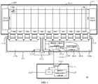
- a display device 10 provided by an embodiment of the invention includes: a display panel 111, a X-board 113, a system board 13 and a connecting part (also referred to as connecting member) CL1.
- the display panel 111 is disposed with a gate driving circuit and a source driving circuit.
- the X-board 113 is disposed with a driving circuit board assembly 1130.
- the display device 10 is an active-matrix display device in the illustrated embodiment, for example, a TCONLESS liquid crystal television (LCD TV).
- a system-on-chip (SOC) disposed on the system board 13 integrates at least part of functions of traditional TCON chip, and the X-board integrates at least another part of the functions of the traditional TCON chip, but the embodiment of the invention is not limited to this.
- the display panel 111 includes a display area 1111, a gate driving circuit electrically connected to the display area 1111 and a source driving circuit electrically connected to the display area 1111.
- the display area 1111 is disposed with a plurality of data lines DL, a plurality of gate lines GL and a plurality of pixels P respectively electrically connected to corresponding one of plurality of data lines DL and corresponding one of the plurality of gate lines GL.
- Each of the plurality of pixels P is located at the intersection of the corresponding gate line GL and the corresponding data line DL.
- the gate driving circuit includes, for example, two GOA (gate on array, gate driving circuit integrated on the array substrate) circuits 1113, which are located on the peripheral area of the display area 1111 and are divided on opposite sides of the display area 1111, that is, the gate driving circuit of the display panel 111 is a bilateral GOA circuit.
- the GOA circuit 1113 is electrically connected to the gate lines GL in the display area 1111 to provide gate driving signals to each of the plurality of gate lines GL in the display area 1111.
- the source driving circuit includes, for example, a plurality of chip-on-flex (COF) type source drivers 1115, such as twelve COF type source drivers 1115 shown in FIG. 1 .
- COF chip-on-flex
- the COF type source driver 1115 is electrically connected to the corresponding data line DL in the display area 1111 and configured to provide an image data signal to each of the plurality of data lines DL. More specifically, one of the plurality of COF type source drivers 1115 includes, for example, a flexible circuit board and a source driver IC disposed on the flexible circuit board.
- the X-board 113 can be a whole independent circuit board or a plurality of circuit sub-boards juxtaposed with each other. If it is the plurality of circuit sub-boards juxtaposed with each other, the driving circuit board assembly 1130 can be disposed on one of the plurality of circuit sub-boards, and adjacent two circuit sub-boards of the plurality of circuit sub-boards form an electrical connection through another connecting part connected between connectors respectively disposed on the adjacent two circuit sub-boards.
- the embodiment is described with two circuit sub-boards.
- the X-board 113 includes two circuit sub-boards 113a and 113b, which are arranged on one side of the display panel 111 along the horizontal direction of FIG. 1 , that is, as a driving circuit board in the row direction; one side of each of the circuit sub-boards 113a and 113b adjacent to the display area 1111 is provided with a connection interface of the COF type source driver 1115, such as a mini-LVDS interface.
- the driving circuit board assembly 1130 is disposed on the circuit sub-board 113a, specifically, the circuit sub-board 113a is provided with a display control circuit 1131, a connector CN1, a nonvolatile memory 1133 and a connector CN3.
- the circuit sub-board 113a is electrically connected to the display area 1111 through a plurality of COF type source drivers 1115, for example, seven COF type source drivers 1115, and electrically connected to the GOA circuit 1113 on the right side of the display panel 111 using the rightmost COF type source driver 1115.
- the circuit sub-board 113b is provided with a connector CN4.
- the circuit sub-board 113b is electrically connected to the display area 1111 through a plurality of COF type source drivers 1115, for example, five COF type source drivers 1115, and electrically connected to the GOA circuit 1113 on the left side of the display panel 111 using the leftmost COF type source driver 1115.
- the connecting part CL2 is, for example, a flexible circuit board or flexible flat cable (FFC), so that the signal generated from the circuit sub-board 113a is transmitted to the circuit sub-board 113b through the connecting part CL2.
- FFC flexible circuit board or flexible flat cable
- the display control circuit 1131 is electrically connected to the first connector CN1, the connector CN3 and a plurality of COF type source drivers 1115, for example, seven COF type source drivers 1115.
- the display control circuit 1131 is not only electrically connected to the seven COF type source drivers 1115 on the right through a printed circuit board (PCB) of the circuit sub-board 113a, but also connected to the five COF type source drivers 1115 on the left through the connector CN3, the connecting part CL2, the connector CN4 and the PCB of the circuit sub-board 113b.
- PCB printed circuit board
- the X-board 113 is also provided with a plurality of mini low voltage differential signaling (Mini-LVDS) interfaces, which are arranged between the COF type source drivers 1115 and the display control circuit 1131, and the first connector includes a point-to-point (P2P) interface.
- Min-LVDS mini low voltage differential signaling
- P2P point-to-point
- the display control circuit 1131 includes a signal conversion circuit 11312, which is electrically connected with the first connector CN1 and the Mini-LVDS interface, and is configured to receive a P2P interface signal containing image data through the first connector, generate source control signals and second interface type image data signals according to the P2P interface signal, and output the source control signals and the second interface type image data signals to the source driving circuit through the plurality of Mini-LVDS interfaces; the second interface type image data signals are Mini-LVDS interface signals.
- a signal conversion circuit 11312 which is electrically connected with the first connector CN1 and the Mini-LVDS interface, and is configured to receive a P2P interface signal containing image data through the first connector, generate source control signals and second interface type image data signals according to the P2P interface signal, and output the source control signals and the second interface type image data signals to the source driving circuit through the plurality of Mini-LVDS interfaces; the second interface type image data signals are Mini-LVDS interface signals.
- the interface of the source driver needs to be adjusted accordingly. For example, if the signal sent by the SOC is transmitted through the P2P interface, the corresponding source driver interface can only use the P2P interface, resulting in an increase in the overall manufacturing cost and test cost.
- the connector CL1 transmits the signal from the SOC to the signal conversion circuit 11312 of the display control circuit 1131 through the P2P interface, the signal conversion circuit 11312 can convert the P2P interface signal into an interface signal corresponding to the panel source driver.
- the interface of the COF type source driver 1115 is the Mini-LVDS interface
- the P2P interface signal is correspondingly converted into the Mini-LVDS signal by the signal conversion circuit
- the Mini-LVDS signal is sent to the interface of the COF type source driver 1115 of the panel, that is, the conversion of the interface signal is completed through the signal conversion circuit 11312, so as to complete the data transmission without changing the original Mini-LVDS interface on the panel.
- the signal conversion circuit for example, in the form of a chip
- the signal conversion circuit 11312 can generate the timing control signals required by the display panel, the debugging and revision of the panel can be completed by the panel manufacturer, and the whole machine manufacturer can reduce the development cost without any change; on the other hand, new panel technology can be completed by the signal conversion circuit 11312, and the system board 13 does not need any change.
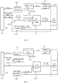
- the display control circuit 1131 further includes a direct-current (DC) voltage conversion circuit 11314, a level conversion circuit 11316 and a Gamma correction circuit 11318.
- the signal conversion circuit 11312 is electrically connected to the connector CN1, the level conversion circuit 11316 and the source driving circuit, and configured to receive reference timing signals such as STV and CKV and a P2P interface signal containing image data (the image data such as RGB data) through the first connector, generate source control signals such as TP and POL and second interface type image data signals such as Mini-LVDS according to the P2P interface signal, and output them to the source driving circuit, and generate initial gate control signals such as ST_in, CKx_in, LC_in and Reset_in according to the reference timing signals such as STV and CKV to the level conversion circuit 11316.
- the DC voltage conversion circuit 11314 is electrically connected to the connector CN1 and configured to receive an input DC voltage such as Vin, and generate gate switching voltages such as VGH and VGL and a reference voltage such as VAA according to the input DC voltage such as Vin, and output the gate switching voltages and the reference voltage to the level conversion circuit 11316 and the Gamma correction circuit 11318 respectively.
- the level conversion circuit 11316 is configured to generate gate control signals such as ST, CKx, LCx and Reset according to the gate switching voltages such as VGH and VGL and the initial gate control signal such as ST_in, CKx_in, LC_in, Reset in to the gate driving circuit.
- the Gamma correction circuit 11318 is configured to generate a plurality of Gamma voltages such as GMAx according to the reference voltage such as VAA to the source driving circuit.
- CKx in is, for example, four high-frequency clock signals CK1 ⁇ CK4, CKx is, for example, eight high-frequency clock signals CK1 ⁇ CK8, and LCx is two low-frequency clock signals LC1 ⁇ LC2 relative to CKx
- GMAx is, for example, fourteen channel Gamma voltages such as GMA1 ⁇ GMA14
- VGH is, for example, + 20V ⁇ + 30V as the gate on voltage
- VGL is, for example, about - 5V as the gate off voltage, but this invention is not limited thereto.
- the P2P interface signal includes multiple pairs of differential signals, which is another interface type different from the Mini-LVDS interface, and is very suitable for short-distance signal transmission from the system board 13 to the circuit sub-board 113a, which can be known mature USI-T, EPI, CMPI and ISP interface, etc.
- the DC voltage conversion circuit 11314 is not limited to generating the above VGH, VGL and VAA, but is also used to provide power supply voltages such as digital voltage VDD and analog voltage HVAA (not shown in the figure) to the signal conversion circuit 11312, the level conversion circuit 11316, the Gamma correction circuit 11318, the gate driving circuit and the source driving circuit.
- the signal conversion circuit 11312, the DC voltage conversion circuit 11314, the level conversion circuit 11316 and the Gamma correction circuit 11318 in the embodiment shown in FIG. 2 are integrated into four different chips, for example.
- the DC voltage conversion circuit 11314 adopts a PMIC chip of known mature technology
- the level conversion circuit 11316 adopts a level shift chip of known mature technology
- the Gamma correction circuit 11318 adopts a P-Gamma chip of known mature technology.
- the DC voltage conversion circuit 11314 and the level conversion circuit 11316 can be integrated on the same chip and the Gamma correction circuit 11318 can be integrated on another chip; or the DC voltage conversion circuit 11314 and the Gamma correction circuit 11318 can be integrated on the same chip and the level conversion circuit 11316 can be integrated on another chip; or the level conversion circuit 11316 and the Gamma correction circuit 11318 can be integrated on the same chip, and the DC voltage conversion circuit 11314 can be integrated on the same chip; or even the DC voltage conversion circuit 11314, the level conversion circuit 11316 and the Gamma correction circuit 11318 can be integrated on the same chip.
- TCON IC Since the functions of TCON IC are integrated in the SOC on the system board, SOC cooperation is required when debugging and changing Panel Timing. However, some functions of TCON IC in the embodiment are set on the X-board. When debugging and changing Panel Timing, it does not depend on the SOC at all and can be developed independently. Through the architecture adjustment of this embodiment, the system board and the X-board can be manufactured and sold separately, and the panel manufacturer can complete the panel debugging and change independently without relying on the change of SOC.
- the display control circuit 1131 includes the Gamma correction circuit 11318
- the Gamma correction circuit 11318 is disposed on the X-board
- the gamma curve can be adjusted piece by piece.
- a power management circuit 135 can also be disposed on the X-board, and the power management circuit 135 is connected to the display control circuit 1131, so that panel manufacturers can adjust and revise the power supply part by themselves during panel manufacturing.
- the display control circuit 1131 cannot include one or more selected from the group consisting of the DC voltage conversion circuit 11314, the level conversion circuit 11316 and the Gamma correction circuit 11318.
- the DC voltage conversion circuit 11314, the level conversion circuit 11316 and the signal conversion circuit 11312 can be integrated into the same chip; alternatively, the DC voltage conversion circuit 11314 and the level conversion circuit 11316 can be integrated on the same chip, and the signal conversion circuit 11312 can be integrated on another chip; alternatively, the DC voltage conversion circuit 11314 and the signal conversion circuit 11312 can be integrated on the same chip, and the level conversion circuit 11316 can be integrated on another chip; alternatively, the level conversion circuit 11316 and the signal conversion circuit 11312 can be integrated on the same chip, and the DC voltage conversion circuit 11314 can be integrated on another chip; alternatively, the DC voltage conversion circuit 11314, the level conversion circuit 11316 and the signal conversion circuit 11312 can be integrated on the same chip.
- the display control circuit 1131 includes a signal conversion circuit 11312, a DC voltage conversion circuit 11314, a level conversion circuit 11316 and a Gamma correction circuit 11318.
- the signal conversion circuit 11312 is electrically connected to the connector CN1 and the source driving circuit and configured to receive the P2P interface signal containing image data through the connector CN1, generate source control signals such as TP and POL and second interface type image data signals such as Mini-LVDS according to the P2P interface signal, and output them to the source driving circuit.
- the DC voltage conversion circuit 11314 is electrically connected to the connector CN1 and configured to receive an input DC voltage such as Vin through the connector CN1, and generate gate switching voltages such as VGH and VGL and a reference voltage such as VAA according to the input DC voltage such as Vin, and output the gate switching voltages and the reference voltage to the level conversion circuit 11316 and the Gamma correction circuit 11318 respectively.
- the level conversion circuit 11316 is electrically connected to the connector CN1 and configured to receive the reference timing signals such as STV and CKV, generate gate control signals such as ST, CKx, LCx and Reset according to the reference timing signals such as STV and CKV and the gate switching voltages such as VGH and VGL to the gate driving circuit.
- the Gamma correction circuit 11318 is configured to generate a plurality of Gamma voltages such as GMAx according to the reference voltage such as VAA to the source driving circuit.
- the reference timing signals such as STV and CKV in the embodiment shown in FIG. 3 are directly sent to the level conversion circuit 11316, rather than initially converted through the signal conversion circuit 11312 and then sent to the level conversion circuit 11316 as shown in FIG. 2 .
- the reference timing signals such as STV and CKV can also be generated locally by the signal conversion circuit 11312 rather than directly provided by the system board 13.
- the display control circuit 1131 can be further electrically connected (not shown in FIG. 1 ) to the nonvolatile memory 1133, for example, connected to the same serial bus as the nonvolatile memory, such as SPI (serial peripheral interface) bus; SPI bus has the advantage of fast data reading and writing speed.
- SPI serial peripheral interface
- the nonvolatile memory 1133 is electrically connected to the connector CN1. As shown in FIG. 4 , the nonvolatile memory 1133 stores an optical performance adjustment parameter table 11330. Parameters contained in the optical performance adjustment parameter table 11330 are parameters strongly related to the optical performance (also referred to as optical characteristics) of the display panel 111.
- the nonvolatile memory 1133 is a SPI interface flash, and accordingly, the connector CN1 includes SPI bus interface.
- the system board 13 is provided with a connector CN2, a system-on-chip 133 and a power management circuit 135.
- the connector CN2 of the system board 13 is connected to the connector CN1 of the circuit sub-board 113a through the connecting part CL1.
- the system-on-chip 133 is electrically connected to the connector CN2 and has an optical performance adjustment intellectual property (IP) core 1330 as shown in FIG. 4 , so that the system-on-chip 133 can read the optical performance adjustment parameter table 11330 stored in the nonvolatile memory of the circuit sub-board 113a by serial communication through the connector CN2, the connecting part CL1 and the connector CN1, and load it into the optical performance adjustment IP core 1330 to adjust the optical performance of the display panel 111.
- IP optical performance adjustment intellectual property
- the connecting part CL1 is, for example, a single flexible cable (FFC).
- the system board 13 of the embodiment is typically provided with a plurality of audio and video input interfaces, such as a CVBS interface, a HDMI interface, etc;
- the system board 13, also known as the mainboard, is used to decode video and audio signals input through the audio and video input interface, and then output the video signal to the X-board in digital signal format.
- the optical performance adjustment IP core 1330 includes: a Demura IP core 1331, a white balance adjustment (also referred to as white tracking adjustment) IP core 1332, a color shift compensation IP core 1333, an OverDrive IP core 1334 and a dithering processing IP core 1335; correspondingly, the optical performance adjustment parameter table 11330 includes a Demura parameter table 11331, a white balance adjustment parameter table 11331, a color shift compensation parameter table 11333, an OverDrive parameter table 11334 and a dithering processing parameter table 11335.
- the Demura IP core 1331 is configured for performing Mura (i.e., a phenomenon of various traces caused by uneven display brightness) elimination (also referred to as Demura) operation according to the Demura parameter table 11331.
- the white balance adjustment IP core 1332 is configured for performing white balance adjustment operation according to the white balance adjustment parameter table 11332.
- the color shift compensation IP core 1333 is configured for performing color shift compensation operation according to the color shift compensation parameter table 11333 to make the display panel 111 achieve low color shift display quality.
- the OverDrive IP core 1334 is configured for performing overvoltage driving (also referred to as OverDrive) operation according to the OverDrive parameter table 11334.
- the dithering processing IP core 1335 is configured for performing dithering processing operation such as temporal dithering and/or spatial dithering according to the dithering processing parameter table 11335.
- dithering processing operation such as temporal dithering and/or spatial dithering according to the dithering processing parameter table 11335.
- the parameters required for the Mura elimination operation, the white balance adjustment operation, the color shift compensation operation, the overvoltage driving operation and the dithering processing operation are known mature technologies, so they will not be repeated here.
- the power management circuit 135 it is electrically connected to the connector CN2 to provide the input DC voltage, such as 12V, to the circuit sub-board 113a; Further, the power management circuit 135 uses, for example, a mature PMIC (Power Management IC).
- the system-on-chip 133 is configured to sequentially control the Demura IP core 1331, the white balance adjustment IP core 1332, the color shift compensation IP core 1333, the OverDrive IP core 1334 and the dithering processing IP core 1335 to perform Demura operation, white balance adjustment, color shift compensation operation, OverDrive operation and dithering processing operation according to the Mura elimination parameter table 11331, the white balance adjustment parameter table 11332, the color shift compensation parameter table 11333, the OverDrive parameter table 11334 and the dithering processing parameter table 11335 respectively.
- This specific optical performance adjustment sequence makes it easier for the display panel 111 to achieve better display quality and optical taste.
- the optical performance adjustment IP core 1330 can also include one or more selected from the group consisting of the Demura IP core 1331, the white balance adjustment IP core 1332, the color shift compensation IP core 1333, the OverDrive IP core 1334 and the dithering processing IP core 1335;
- the optical performance adjustment parameter table 11330 can include one or more selected from the group consisting of the Mura elimination parameter table 11331, the white balance adjustment parameter table 11332, the color shift compensation parameter table 11333, the OverDrive parameter table 11334 and the dithering processing parameter table 11335 respectively.
- optical performance adjustment parameters also referred to as optical codes
- debugging of each parameter in the optical performance adjustment parameter table is changed from the whole machine manufacturer to the panel manufacturer; because the optical performance adjustment parameters are strongly related to the panel, the optical performance adjustment parameter tables required for different panels are different, and the panel manufacturers know more about the optical characteristics of their own panels. Therefore, they can flexibly adjust the panel optical characteristics according to their own panel characteristics, which can liberate the whole machine manufacturers from the tedious work of adjusting optical characteristics, so as to accelerate the development speed of the whole machine.
- the foregoing embodiments are only exemplary descriptions of the invention. On the premise that the technical features do not conflict, the structure does not conflict and does not violate the purpose of the invention, the technical solutions of the embodiments can be combined and used arbitrarily. Further, it can be understood that the signal conversion circuit 11312, the DC voltage conversion circuit 11314, the level conversion circuit 11316 and the Gamma correction circuit 11318 of the display control circuit 1131 in the foregoing embodiments are not limited to being distributed on a single circuit sub-board 113a, but can also be distributed on a plurality of driving circuit boards, such as circuit sub-boards 113a and 113b in FIG. 1 .
- the above display devices can be: LTPO (Low Temperature Polycrystalline Oxide) display device, Micro LED display device, liquid crystal panel, electronic paper, OLED (Organic Light-Emitting Diode) panel, AMOLED (Active-Matrix Organic Light Emitting Diode) panel, mobile phone, tablet computer, TV, display, notebook computer, digital photo frame and other products or components with display function.
- LTPO Low Temperature Polycrystalline Oxide
- Micro LED display device liquid crystal panel
- electronic paper electronic paper
- OLED (Organic Light-Emitting Diode) panel OLED (Organic Light-Emitting Diode) panel
- AMOLED Active-Matrix Organic Light Emitting Diode
- the illustrated system, device, and method may be implemented in other manners.
- the embodiments of device described above are merely illustrative, for example, the division of units is only a logical function division, and in actual implementations there may be another division manner, for example, multiple units or components may be combined or integrated into another system, or some features can be ignored or not executed.
- the coupling or direct coupling or communication connection as illustrated may be an indirect coupling or communication connection through some interfaces, devices or units, and further may be in an electrical, mechanical or other form.
- the units described as separate components may be or may not be physically separated, and the components illustrated as units may be or may not be physical units, that is, may be located in one place, or may be distributed to multiple network units. Some or all of the units may be selected according to actual needs to achieve the purposes of the solutions of the embodiments.
- each functional unit in each embodiment of the invention may be integrated into one processing unit, or each unit may be physically separated, or two or more units may be integrated into one unit.
- the above integrated unit can be implemented in a form of hardware or in a form of hardware with a software functional unit(s).
- the above integrated unit implemented in the form of the software functional unit(s) can be stored in a computer readable storage medium.
- the above software functional unit(s) is/are stored in a storage medium and include(s) several instructions for causing a computer device (which may be a personal computer, a server, or a network device, etc.) to perform some of the steps of various embodiments of the invention.
- a computer device which may be a personal computer, a server, or a network device, etc.
- the foregoing storage medium may be a U-disk, a mobile hard disk, a read-only memory (ROM), a random-access memory (RAM), a magnetic disk, or an optical disk, which can store program codes.
Landscapes
- Engineering & Computer Science (AREA)
- Physics & Mathematics (AREA)
- Computer Hardware Design (AREA)
- General Physics & Mathematics (AREA)
- Theoretical Computer Science (AREA)
- Chemical & Material Sciences (AREA)
- Crystallography & Structural Chemistry (AREA)
- Control Of Indicators Other Than Cathode Ray Tubes (AREA)
Applications Claiming Priority (3)
| Application Number | Priority Date | Filing Date | Title |
|---|---|---|---|
| CN201910557272 | 2019-06-25 | ||
| PCT/CN2019/095757 WO2020258392A1 (fr) | 2019-06-25 | 2019-07-12 | Appareil d'affichage à matrice active et composant de carte de circuit de pilotage |
| PCT/CN2019/097161 WO2020258428A1 (fr) | 2019-06-25 | 2019-07-22 | Dispositif d'affichage |
Publications (3)
| Publication Number | Publication Date |
|---|---|
| EP3985657A1 true EP3985657A1 (fr) | 2022-04-20 |
| EP3985657A4 EP3985657A4 (fr) | 2022-08-10 |
| EP3985657B1 EP3985657B1 (fr) | 2025-06-25 |
Family
ID=73849541
Family Applications (1)
| Application Number | Title | Priority Date | Filing Date |
|---|---|---|---|
| EP19934878.0A Active EP3985657B1 (fr) | 2019-06-25 | 2019-07-22 | Dispositif d'affichage |
Country Status (3)
| Country | Link |
|---|---|
| EP (1) | EP3985657B1 (fr) |
| CN (1) | CN112133256A (fr) |
| WO (1) | WO2020258428A1 (fr) |
Cited By (1)
| Publication number | Priority date | Publication date | Assignee | Title |
|---|---|---|---|---|
| EP4207173A1 (fr) * | 2021-12-30 | 2023-07-05 | SES-imagotag | Dispositif d'affichage de papier électronique |
Families Citing this family (5)
| Publication number | Priority date | Publication date | Assignee | Title |
|---|---|---|---|---|
| CN113539137B (zh) * | 2020-04-09 | 2023-07-25 | 咸阳彩虹光电科技有限公司 | 新型显示装置、显示系统 |
| CN116413971A (zh) * | 2021-12-30 | 2023-07-11 | 思电子系统意象公司 | 电子纸显示装置 |
| CN115048335B (zh) * | 2022-06-21 | 2024-09-03 | 中国船舶集团有限公司第七二三研究所 | 一种基于国产器件的采集显示电路及其工作方法 |
| CN114927114B (zh) * | 2022-06-29 | 2024-04-09 | 高创(苏州)电子有限公司 | 显示装置输入电路、显示装置及其控制方法 |
| WO2025145269A1 (fr) * | 2024-01-02 | 2025-07-10 | 京东方科技集团股份有限公司 | Module d'affichage et dispositif d'affichage |
Family Cites Families (16)
| Publication number | Priority date | Publication date | Assignee | Title |
|---|---|---|---|---|
| KR20080028092A (ko) * | 2006-09-26 | 2008-03-31 | 삼성에스디아이 주식회사 | 플라즈마 표시 장치 및 그 구동 장치와 그 구동 방법 |
| KR101286541B1 (ko) * | 2008-05-19 | 2013-07-23 | 엘지디스플레이 주식회사 | 액정표시장치 |
| KR101289642B1 (ko) * | 2009-05-11 | 2013-07-30 | 엘지디스플레이 주식회사 | 액정표시장치 |
| CN101996544A (zh) * | 2010-09-28 | 2011-03-30 | 天津三星电子显示器有限公司 | 实现显示器图像处理与时序控制芯片一体化的方法 |
| CN202159474U (zh) * | 2011-06-27 | 2012-03-07 | 深圳市华星光电技术有限公司 | 液晶面板的数据驱动系统和芯片、以及液晶显示装置 |
| KR101981558B1 (ko) * | 2011-10-24 | 2019-05-24 | 엘지디스플레이 주식회사 | 액정표시장치 |
| JP2014010762A (ja) * | 2012-07-02 | 2014-01-20 | Japan Display Inc | 表示装置 |
| KR102055152B1 (ko) * | 2012-10-12 | 2019-12-12 | 엘지디스플레이 주식회사 | 표시장치 |
| CN103745703A (zh) * | 2013-12-31 | 2014-04-23 | 深圳市华星光电技术有限公司 | 一种液晶面板的驱动电路、液晶面板和液晶显示装置 |
| CN105679268B (zh) * | 2016-03-29 | 2019-01-08 | 硅谷数模半导体(北京)有限公司 | 显示组件 |
| CN107241562B (zh) * | 2017-07-25 | 2020-09-22 | 四川长虹电器股份有限公司 | 超高清液晶电视电路系统及接口 |
| CN107396022B (zh) * | 2017-08-22 | 2020-12-29 | Tcl华星光电技术有限公司 | 数据传输装置及液晶显示装置 |
| CN107342060B (zh) * | 2017-09-13 | 2019-12-27 | 京东方科技集团股份有限公司 | 驱动芯片和显示装置 |
| CN208126060U (zh) * | 2018-04-28 | 2018-11-20 | 咸阳彩虹光电科技有限公司 | 显示面板的非对称驱动装置以及显示装置 |
| CN108648712A (zh) * | 2018-06-12 | 2018-10-12 | 广东长虹电子有限公司 | 一种应用于液晶屏的tcon板与source板连接电路 |
| CN208538435U (zh) * | 2018-08-01 | 2019-02-22 | 京东方科技集团股份有限公司 | 一种显示装置 |
-
2019
- 2019-07-22 WO PCT/CN2019/097161 patent/WO2020258428A1/fr not_active Ceased
- 2019-07-22 EP EP19934878.0A patent/EP3985657B1/fr active Active
- 2019-07-22 CN CN201910662882.0A patent/CN112133256A/zh active Pending
Cited By (1)
| Publication number | Priority date | Publication date | Assignee | Title |
|---|---|---|---|---|
| EP4207173A1 (fr) * | 2021-12-30 | 2023-07-05 | SES-imagotag | Dispositif d'affichage de papier électronique |
Also Published As
| Publication number | Publication date |
|---|---|
| WO2020258428A1 (fr) | 2020-12-30 |
| EP3985657A4 (fr) | 2022-08-10 |
| CN112133256A (zh) | 2020-12-25 |
| EP3985657B1 (fr) | 2025-06-25 |
Similar Documents
| Publication | Publication Date | Title |
|---|---|---|
| EP3985657B1 (fr) | Dispositif d'affichage | |
| KR101289642B1 (ko) | 액정표시장치 | |
| US11620930B2 (en) | Display device with system-on-chip including optical performance adjustment IP core | |
| KR20080084389A (ko) | 액정표시장치 | |
| US8004487B2 (en) | Display device | |
| CN111199716B (zh) | 显示设备及驱动显示设备的方法 | |
| KR101542239B1 (ko) | 표시장치 | |
| US20090002305A1 (en) | Liquid crystal display with common voltage generator for reducing crosstalk | |
| KR20110132723A (ko) | 액정표시장치 및 그 구동방법과 제조방법 | |
| KR101633103B1 (ko) | 액정표시장치 | |
| CN112992079B (zh) | 改善显示画质的方法及显示装置 | |
| KR102364096B1 (ko) | 표시장치 | |
| CN114495851B (zh) | 显示装置 | |
| KR101595463B1 (ko) | 액정 표시장치 | |
| WO2025140633A1 (fr) | Carte de circuit intégré, appareil d'affichage, dispositif d'affichage et procédé d'affichage | |
| CN220553284U (zh) | 一种288分区Mini LED背光驱动电路 | |
| CN116741114B (zh) | 显示模组 | |
| KR101761407B1 (ko) | 액정표시장치 | |
| KR101773194B1 (ko) | 표시장치 | |
| CN112992086A (zh) | 一种显示装置、连接组件 | |
| KR101968178B1 (ko) | 타이밍 제어부 및 이를 포함하는 액정표시장치 | |
| CN107799046A (zh) | 显示装置和控制器 | |
| KR20080088022A (ko) | 액정표시장치 | |
| CN120319165B (zh) | 数据处理电路、显示装置及数据处理方法 | |
| KR20130031102A (ko) | 전원공급장치 및 전원공급방법. |
Legal Events
| Date | Code | Title | Description |
|---|---|---|---|
| STAA | Information on the status of an ep patent application or granted ep patent |
Free format text: STATUS: THE INTERNATIONAL PUBLICATION HAS BEEN MADE |
|
| PUAI | Public reference made under article 153(3) epc to a published international application that has entered the european phase |
Free format text: ORIGINAL CODE: 0009012 |
|
| STAA | Information on the status of an ep patent application or granted ep patent |
Free format text: STATUS: REQUEST FOR EXAMINATION WAS MADE |
|
| 17P | Request for examination filed |
Effective date: 20220117 |
|
| AK | Designated contracting states |
Kind code of ref document: A1 Designated state(s): AL AT BE BG CH CY CZ DE DK EE ES FI FR GB GR HR HU IE IS IT LI LT LU LV MC MK MT NL NO PL PT RO RS SE SI SK SM TR |
|
| A4 | Supplementary search report drawn up and despatched |
Effective date: 20220712 |
|
| RIC1 | Information provided on ipc code assigned before grant |
Ipc: G09G 3/20 20060101ALI20220706BHEP Ipc: G09G 3/36 20060101AFI20220706BHEP |
|
| DAV | Request for validation of the european patent (deleted) | ||
| DAX | Request for extension of the european patent (deleted) | ||
| STAA | Information on the status of an ep patent application or granted ep patent |
Free format text: STATUS: EXAMINATION IS IN PROGRESS |
|
| 17Q | First examination report despatched |
Effective date: 20241202 |
|
| GRAP | Despatch of communication of intention to grant a patent |
Free format text: ORIGINAL CODE: EPIDOSNIGR1 |
|
| STAA | Information on the status of an ep patent application or granted ep patent |
Free format text: STATUS: GRANT OF PATENT IS INTENDED |
|
| INTG | Intention to grant announced |
Effective date: 20250414 |
|
| GRAS | Grant fee paid |
Free format text: ORIGINAL CODE: EPIDOSNIGR3 |
|
| GRAA | (expected) grant |
Free format text: ORIGINAL CODE: 0009210 |
|
| STAA | Information on the status of an ep patent application or granted ep patent |
Free format text: STATUS: THE PATENT HAS BEEN GRANTED |
|
| AK | Designated contracting states |
Kind code of ref document: B1 Designated state(s): AL AT BE BG CH CY CZ DE DK EE ES FI FR GB GR HR HU IE IS IT LI LT LU LV MC MK MT NL NO PL PT RO RS SE SI SK SM TR |
|
| REG | Reference to a national code |
Ref country code: GB Ref legal event code: FG4D |
|
| REG | Reference to a national code |
Ref country code: CH Ref legal event code: EP |
|
| REG | Reference to a national code |
Ref country code: CH Ref legal event code: EP |
|
| REG | Reference to a national code |
Ref country code: IE Ref legal event code: FG4D |
|
| REG | Reference to a national code |
Ref country code: DE Ref legal event code: R096 Ref document number: 602019071791 Country of ref document: DE |
|
| PG25 | Lapsed in a contracting state [announced via postgrant information from national office to epo] |
Ref country code: FI Free format text: LAPSE BECAUSE OF FAILURE TO SUBMIT A TRANSLATION OF THE DESCRIPTION OR TO PAY THE FEE WITHIN THE PRESCRIBED TIME-LIMIT Effective date: 20250625 |
|
| PGFP | Annual fee paid to national office [announced via postgrant information from national office to epo] |
Ref country code: DE Payment date: 20250711 Year of fee payment: 7 |
|
| REG | Reference to a national code |
Ref country code: LT Ref legal event code: MG9D |
|
| PG25 | Lapsed in a contracting state [announced via postgrant information from national office to epo] |
Ref country code: NO Free format text: LAPSE BECAUSE OF FAILURE TO SUBMIT A TRANSLATION OF THE DESCRIPTION OR TO PAY THE FEE WITHIN THE PRESCRIBED TIME-LIMIT Effective date: 20250925 Ref country code: GR Free format text: LAPSE BECAUSE OF FAILURE TO SUBMIT A TRANSLATION OF THE DESCRIPTION OR TO PAY THE FEE WITHIN THE PRESCRIBED TIME-LIMIT Effective date: 20250926 |
|
| PG25 | Lapsed in a contracting state [announced via postgrant information from national office to epo] |
Ref country code: BG Free format text: LAPSE BECAUSE OF FAILURE TO SUBMIT A TRANSLATION OF THE DESCRIPTION OR TO PAY THE FEE WITHIN THE PRESCRIBED TIME-LIMIT Effective date: 20250625 |
|
| PGFP | Annual fee paid to national office [announced via postgrant information from national office to epo] |
Ref country code: GB Payment date: 20250704 Year of fee payment: 7 |
|
| PG25 | Lapsed in a contracting state [announced via postgrant information from national office to epo] |
Ref country code: HR Free format text: LAPSE BECAUSE OF FAILURE TO SUBMIT A TRANSLATION OF THE DESCRIPTION OR TO PAY THE FEE WITHIN THE PRESCRIBED TIME-LIMIT Effective date: 20250625 |
|
| PGFP | Annual fee paid to national office [announced via postgrant information from national office to epo] |
Ref country code: FR Payment date: 20250730 Year of fee payment: 7 |
|
| PG25 | Lapsed in a contracting state [announced via postgrant information from national office to epo] |
Ref country code: RS Free format text: LAPSE BECAUSE OF FAILURE TO SUBMIT A TRANSLATION OF THE DESCRIPTION OR TO PAY THE FEE WITHIN THE PRESCRIBED TIME-LIMIT Effective date: 20250925 |
|
| PG25 | Lapsed in a contracting state [announced via postgrant information from national office to epo] |
Ref country code: LV Free format text: LAPSE BECAUSE OF FAILURE TO SUBMIT A TRANSLATION OF THE DESCRIPTION OR TO PAY THE FEE WITHIN THE PRESCRIBED TIME-LIMIT Effective date: 20250625 |
|
| REG | Reference to a national code |
Ref country code: NL Ref legal event code: MP Effective date: 20250625 |
|
| PG25 | Lapsed in a contracting state [announced via postgrant information from national office to epo] |
Ref country code: NL Free format text: LAPSE BECAUSE OF FAILURE TO SUBMIT A TRANSLATION OF THE DESCRIPTION OR TO PAY THE FEE WITHIN THE PRESCRIBED TIME-LIMIT Effective date: 20250625 |
|
| PG25 | Lapsed in a contracting state [announced via postgrant information from national office to epo] |
Ref country code: PT Free format text: LAPSE BECAUSE OF FAILURE TO SUBMIT A TRANSLATION OF THE DESCRIPTION OR TO PAY THE FEE WITHIN THE PRESCRIBED TIME-LIMIT Effective date: 20251027 |
|
| REG | Reference to a national code |
Ref country code: AT Ref legal event code: MK05 Ref document number: 1807400 Country of ref document: AT Kind code of ref document: T Effective date: 20250625 |
|
| PG25 | Lapsed in a contracting state [announced via postgrant information from national office to epo] |
Ref country code: IS Free format text: LAPSE BECAUSE OF FAILURE TO SUBMIT A TRANSLATION OF THE DESCRIPTION OR TO PAY THE FEE WITHIN THE PRESCRIBED TIME-LIMIT Effective date: 20251025 |
|
| PG25 | Lapsed in a contracting state [announced via postgrant information from national office to epo] |
Ref country code: AT Free format text: LAPSE BECAUSE OF FAILURE TO SUBMIT A TRANSLATION OF THE DESCRIPTION OR TO PAY THE FEE WITHIN THE PRESCRIBED TIME-LIMIT Effective date: 20250625 Ref country code: SM Free format text: LAPSE BECAUSE OF FAILURE TO SUBMIT A TRANSLATION OF THE DESCRIPTION OR TO PAY THE FEE WITHIN THE PRESCRIBED TIME-LIMIT Effective date: 20250625 |
|
| PG25 | Lapsed in a contracting state [announced via postgrant information from national office to epo] |
Ref country code: CZ Free format text: LAPSE BECAUSE OF FAILURE TO SUBMIT A TRANSLATION OF THE DESCRIPTION OR TO PAY THE FEE WITHIN THE PRESCRIBED TIME-LIMIT Effective date: 20250625 |
|
| PG25 | Lapsed in a contracting state [announced via postgrant information from national office to epo] |
Ref country code: PL Free format text: LAPSE BECAUSE OF FAILURE TO SUBMIT A TRANSLATION OF THE DESCRIPTION OR TO PAY THE FEE WITHIN THE PRESCRIBED TIME-LIMIT Effective date: 20250625 |
|
| PG25 | Lapsed in a contracting state [announced via postgrant information from national office to epo] |
Ref country code: EE Free format text: LAPSE BECAUSE OF FAILURE TO SUBMIT A TRANSLATION OF THE DESCRIPTION OR TO PAY THE FEE WITHIN THE PRESCRIBED TIME-LIMIT Effective date: 20250625 |
|
| PG25 | Lapsed in a contracting state [announced via postgrant information from national office to epo] |
Ref country code: SK Free format text: LAPSE BECAUSE OF FAILURE TO SUBMIT A TRANSLATION OF THE DESCRIPTION OR TO PAY THE FEE WITHIN THE PRESCRIBED TIME-LIMIT Effective date: 20250625 |
|
| PG25 | Lapsed in a contracting state [announced via postgrant information from national office to epo] |
Ref country code: ES Free format text: LAPSE BECAUSE OF FAILURE TO SUBMIT A TRANSLATION OF THE DESCRIPTION OR TO PAY THE FEE WITHIN THE PRESCRIBED TIME-LIMIT Effective date: 20250625 |
|
| REG | Reference to a national code |
Ref country code: CH Ref legal event code: H13 Free format text: ST27 STATUS EVENT CODE: U-0-0-H10-H13 (AS PROVIDED BY THE NATIONAL OFFICE) Effective date: 20260224 |
|
| PG25 | Lapsed in a contracting state [announced via postgrant information from national office to epo] |
Ref country code: LU Free format text: LAPSE BECAUSE OF NON-PAYMENT OF DUE FEES Effective date: 20250722 Ref country code: RO Free format text: LAPSE BECAUSE OF FAILURE TO SUBMIT A TRANSLATION OF THE DESCRIPTION OR TO PAY THE FEE WITHIN THE PRESCRIBED TIME-LIMIT Effective date: 20250625 |
|
| REG | Reference to a national code |
Ref country code: BE Ref legal event code: MM Effective date: 20250731 |
|
| PG25 | Lapsed in a contracting state [announced via postgrant information from national office to epo] |
Ref country code: MC Free format text: LAPSE BECAUSE OF FAILURE TO SUBMIT A TRANSLATION OF THE DESCRIPTION OR TO PAY THE FEE WITHIN THE PRESCRIBED TIME-LIMIT Effective date: 20250625 |
|
| PG25 | Lapsed in a contracting state [announced via postgrant information from national office to epo] |
Ref country code: DK Free format text: LAPSE BECAUSE OF FAILURE TO SUBMIT A TRANSLATION OF THE DESCRIPTION OR TO PAY THE FEE WITHIN THE PRESCRIBED TIME-LIMIT Effective date: 20250625 |
|
| PG25 | Lapsed in a contracting state [announced via postgrant information from national office to epo] |
Ref country code: BE Free format text: LAPSE BECAUSE OF NON-PAYMENT OF DUE FEES Effective date: 20250731 Ref country code: IT Free format text: LAPSE BECAUSE OF FAILURE TO SUBMIT A TRANSLATION OF THE DESCRIPTION OR TO PAY THE FEE WITHIN THE PRESCRIBED TIME-LIMIT Effective date: 20250625 |
|
| PG25 | Lapsed in a contracting state [announced via postgrant information from national office to epo] |
Ref country code: CH Free format text: LAPSE BECAUSE OF NON-PAYMENT OF DUE FEES Effective date: 20250731 |
|
| PLBE | No opposition filed within time limit |
Free format text: ORIGINAL CODE: 0009261 |
|
| STAA | Information on the status of an ep patent application or granted ep patent |
Free format text: STATUS: NO OPPOSITION FILED WITHIN TIME LIMIT |