EP3985672A1 - Structure semi-conductrice, et son procédé de fabrication et son procédé de commande - Google Patents
Structure semi-conductrice, et son procédé de fabrication et son procédé de commande Download PDFInfo
- Publication number
- EP3985672A1 EP3985672A1 EP21773442.5A EP21773442A EP3985672A1 EP 3985672 A1 EP3985672 A1 EP 3985672A1 EP 21773442 A EP21773442 A EP 21773442A EP 3985672 A1 EP3985672 A1 EP 3985672A1
- Authority
- EP
- European Patent Office
- Prior art keywords
- insulator
- base substrate
- source
- semiconductor structure
- facing away
- Prior art date
- Legal status (The legal status is an assumption and is not a legal conclusion. Google has not performed a legal analysis and makes no representation as to the accuracy of the status listed.)
- Granted
Links
Images










Classifications
-
- H—ELECTRICITY
- H10—SEMICONDUCTOR DEVICES; ELECTRIC SOLID-STATE DEVICES NOT OTHERWISE PROVIDED FOR
- H10B—ELECTRONIC MEMORY DEVICES
- H10B12/00—Dynamic random access memory [DRAM] devices
- H10B12/01—Manufacture or treatment
- H10B12/02—Manufacture or treatment for one transistor one-capacitor [1T-1C] memory cells
- H10B12/05—Making the transistor
-
- G—PHYSICS
- G11—INFORMATION STORAGE
- G11C—STATIC STORES
- G11C11/00—Digital stores characterised by the use of particular electric or magnetic storage elements; Storage elements therefor
- G11C11/21—Digital stores characterised by the use of particular electric or magnetic storage elements; Storage elements therefor using electric elements
- G11C11/34—Digital stores characterised by the use of particular electric or magnetic storage elements; Storage elements therefor using electric elements using semiconductor devices
- G11C11/40—Digital stores characterised by the use of particular electric or magnetic storage elements; Storage elements therefor using electric elements using semiconductor devices using transistors
- G11C11/401—Digital stores characterised by the use of particular electric or magnetic storage elements; Storage elements therefor using electric elements using semiconductor devices using transistors forming cells needing refreshing or charge regeneration, i.e. dynamic cells
- G11C11/4063—Auxiliary circuits, e.g. for addressing, decoding, driving, writing, sensing or timing
- G11C11/407—Auxiliary circuits, e.g. for addressing, decoding, driving, writing, sensing or timing for memory cells of the field-effect type
- G11C11/408—Address circuits
- G11C11/4085—Word line control circuits, e.g. word line drivers, - boosters, - pull-up, - pull-down, - precharge
-
- H—ELECTRICITY
- H10—SEMICONDUCTOR DEVICES; ELECTRIC SOLID-STATE DEVICES NOT OTHERWISE PROVIDED FOR
- H10B—ELECTRONIC MEMORY DEVICES
- H10B12/00—Dynamic random access memory [DRAM] devices
- H10B12/30—DRAM devices comprising one-transistor - one-capacitor [1T-1C] memory cells
- H10B12/31—DRAM devices comprising one-transistor - one-capacitor [1T-1C] memory cells having a storage electrode stacked over the transistor
- H10B12/315—DRAM devices comprising one-transistor - one-capacitor [1T-1C] memory cells having a storage electrode stacked over the transistor with the capacitor higher than a bit line
-
- H—ELECTRICITY
- H10—SEMICONDUCTOR DEVICES; ELECTRIC SOLID-STATE DEVICES NOT OTHERWISE PROVIDED FOR
- H10B—ELECTRONIC MEMORY DEVICES
- H10B12/00—Dynamic random access memory [DRAM] devices
- H10B12/30—DRAM devices comprising one-transistor - one-capacitor [1T-1C] memory cells
- H10B12/48—Data lines or contacts therefor
- H10B12/482—Bit lines
-
- H—ELECTRICITY
- H10—SEMICONDUCTOR DEVICES; ELECTRIC SOLID-STATE DEVICES NOT OTHERWISE PROVIDED FOR
- H10B—ELECTRONIC MEMORY DEVICES
- H10B12/00—Dynamic random access memory [DRAM] devices
- H10B12/30—DRAM devices comprising one-transistor - one-capacitor [1T-1C] memory cells
- H10B12/48—Data lines or contacts therefor
- H10B12/488—Word lines
-
- H—ELECTRICITY
- H10—SEMICONDUCTOR DEVICES; ELECTRIC SOLID-STATE DEVICES NOT OTHERWISE PROVIDED FOR
- H10D—INORGANIC ELECTRIC SEMICONDUCTOR DEVICES
- H10D30/00—Field-effect transistors [FET]
- H10D30/01—Manufacture or treatment
- H10D30/021—Manufacture or treatment of FETs having insulated gates [IGFET]
- H10D30/025—Manufacture or treatment of FETs having insulated gates [IGFET] of vertical IGFETs
-
- H—ELECTRICITY
- H10—SEMICONDUCTOR DEVICES; ELECTRIC SOLID-STATE DEVICES NOT OTHERWISE PROVIDED FOR
- H10D—INORGANIC ELECTRIC SEMICONDUCTOR DEVICES
- H10D30/00—Field-effect transistors [FET]
- H10D30/60—Insulated-gate field-effect transistors [IGFET]
- H10D30/63—Vertical IGFETs
-
- H—ELECTRICITY
- H10—SEMICONDUCTOR DEVICES; ELECTRIC SOLID-STATE DEVICES NOT OTHERWISE PROVIDED FOR
- H10B—ELECTRONIC MEMORY DEVICES
- H10B12/00—Dynamic random access memory [DRAM] devices
- H10B12/01—Manufacture or treatment
- H10B12/02—Manufacture or treatment for one transistor one-capacitor [1T-1C] memory cells
- H10B12/03—Making the capacitor or connections thereto
- H10B12/033—Making the capacitor or connections thereto the capacitor extending over the transistor
- H10B12/0335—Making a connection between the transistor and the capacitor, e.g. plug
Definitions
- the disclosure relates to the technical field of storage, and in particular to a semiconductor structure, and a manufacturing method and control method thereof.
- a memory generally includes multiple memory cells. Each memory cell includes a switch transistor and a capacitor.
- the memory generally provides a turn-off or turn-on signal to a gate of the switch transistor through a word line, and is connected with a source or drain of the switch transistor through a bit line to provide logic "1" or "0" to the capacitor through the switch transistor.
- the memory integrates the word line, the bit line, the switch transistor, and the capacitor on the same semiconductor structure.
- the integration density of the switch transistor in the semiconductor structure is relatively low, thereby influencing the number of the memory cells in the semiconductor structure in unit size.
- a semiconductor structure including: a base substrate, multiple bit lines, multiple active bodies, an insulator, and multiple word lines.
- the insulator is located on one side of the base substrate; the multiple bit lines are arranged in the insulator, and the multiple bit lines are distributed at intervals along a first direction and extend along a second direction; the multiple active bodies are located in the insulator, the active bodies are located on sides of respective bit lines facing away from the base substrate, orthographic projection of each active body on the base substrate at least partially coincides with the orthographic projection of a respective bit line on the base substrate, and the active bodies are distributed at intervals along the second direction; the multiple word lines are located in the insulator and located on sides of respective bit lines facing away from the base substrate, the word lines are distributed at intervals along the second direction and extend along the first direction, and only one word line is arranged between two adjacent active bodies in the second direction.
- each active body includes: a first source or drain part, an active part and a second source or drain part.
- the first source or drain part is located on one side of a respective bit line facing away from the base substrate; the active part is located on one side of the first source or drain part facing away from the substrate base plat; and the second source or drain part is located on one side of the active part facing away from the base substrate.
- the insulator includes: a first insulator, a second insulator, and a third insulator.
- the first insulator is located between each word line and a respective active body; the second insulator is located on one side of each word line facing away from the base substrate; and the third insulator is located between each word line and a respective bit line.
- material of the first insulator is silicon oxide
- the material of the second insulator is silicon nitride
- the first direction is perpendicular to the second direction.
- each bit line and the base substrate are arranged to be insulated from one another through a respective part of the insulator.
- the first source or drain part and the second source or drain part are doped polysilicon conductors, and a material of the active part is polysilicon.
- the semiconductor structure further includes a first conductor part and a second conductor part.
- the first conductor part is located between each bit line and the first source or drain part; and the second conductor part is located on one side of the second source or drain part facing away from the base substrate.
- a manufacturing method of a semiconductor structure including the following operations.
- a to-be-etched body is formed.
- the to-be-etched body includes a base substrate, an insulator located on one side of the base substrate and multiple bit lines.
- the bit lines are located in the insulator, and the multiple bit lines are distributed at intervals along a first direction and extend along a second direction.
- Multiple second grooves which are distributed at intervals along the second direction and extend along the first direction are formed on one side of the insulator facing away from the bit lines.
- a word line and a fourth insulating layer are sequentially formed in each second groove.
- the fourth insulating layer is located on one side of the word line facing away from a bottom of the second groove.
- Orthographic projection of each through hole on the base substrate at least partially coincides with the orthographic projection of a respective bit line on the base substrate.
- the through hole extends to a surface of one side of the bit line facing the through hole.
- the orthographic projection of each through hole on the base substrate is located between the orthographic projections of two adjacent word lines on the base substrate. In the second direction, the orthographic projection of only one word line on the base substrate is located between the orthographic projections of two adjacent through holes on the base substrate.
- a fifth insulating layer is formed on one side of the word line exposed to the through hole.
- a first source or drain part, an active part and a second source or drain part are formed in each through hole.
- the first source or drain part is located on one side of the bit line
- the active part is located on one side of the first source or drain part facing away from the bit line
- the second source or drain part is located on one side of the active part facing away from the bit line.
- the operation that a to-be-etched body is formed includes the following operations.
- a substrate material layer is formed.
- Multiple first grooves which are distributed at intervals along the first direction and extend along the second direction, are formed on one side surface of the substrate material layer.
- a first insulating layer, a bit line and a second insulating layer are formed in the first groove.
- the bit line is located on one side of the first insulating layer facing away from a bottom of the first groove.
- the second insulating layer is located on one side of the bit line facing away from the bottom of the first groove.
- the substrate material layer on one side, facing an opening of the first groove, of a plane of the bottom of the first groove is removed so as to form the remaining substrate material layer into the base substrate, and a third insulating layer is filled at a position of a removed substrate material layer so as to form the third insulating layer, the first insulating layer and the second insulating layer into the insulator.
- a first conductor part is formed in the through hole.
- the first conductor part is located between each bit line and the first source or drain part.
- a second conductor part is formed in the through hole.
- the second conductor part is located on one side of the second source or drain part facing away from the base substrate.
- a control method of a semiconductor structure is provided.
- the method is configured to control the semiconductor structure and includes the following operation.
- a turn-on signal is simultaneously input to two adjacent word lines to turn on an active body located between the two word lines.
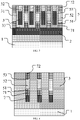
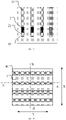
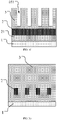
- FIG. 1 is a top perspective view of one exemplary embodiment of a semiconductor structure of the disclosure.
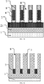
- FIG. 2 is a cross-sectional view along a dotted line A-A in FIG. 1 .
- FIG. 3 is a cross-sectional view along a dotted line B-B in FIG. 1 .
- the semiconductor structure includes: a base substrate 1, multiple bit lines 2, multiple active bodies 5, an insulator 3, and multiple word lines 4.
- the insulator 3 is located on one side of the base substrate 1; the multiple bit lines 2 are arranged in the insulator 3, and the multiple bit lines 2 are distributed at intervals along a first direction X and extend along a second direction Y; the multiple active bodies 5 are located in the insulator 3, the active bodies 5 are located on sides of respective bit lines 2 facing away from the base substrate 1, orthographic projection of each active body 5 on the base substrate 1 at least partially coincides with the orthographic projection of a respective bit line 2 on the base substrate, and the active bodies are distributed at intervals along the second direction Y; the multiple word lines 4 are located in the insulator 3 and located on sides of respective bit lines 2 facing away from the base substrate 1, the word lines 4 are distributed at intervals along the second direction Y and extend along the first direction X, and only one word line 4 is arranged between two adjacent active bodies 5 in the second direction Y.
- the word line 4 may be insulated from the active body 5 and the bit line 2 through a part of the insulator 3.
- each active body 5 may include: a first source or drain part 51, an active part 52, and a second source or drain part 53.
- the first source or drain part 51 may be located on one side of a respective bit line 2 facing away from the base substrate 1; the active part 52 may be located on one side of the first source or drain part 51 facing away from the base substrate 1; and the second source or drain part 53 may be located on one side of the active part 52 facing away from the base substrate 1.
- the active body 5 may form a source or drain and a channel region of one switch transistor, and a part of the word line 4 may form a gate of the switch transistor.
- One side of the second source or drain part 53 facing away from the base substrate 1 may be exposed to outside the insulator, and a capacitor may also be arranged on one side of the second source or drain part 53 facing away from the base substrate 1 in order to form multiple memory cells distributed in an array on the semiconductor structure.
- Each memory cell may include one switch transistor and one capacitor.
- the semiconductor structure provided by the disclosure only one word line 4 is arranged between two adjacent active bodies 5 in the second direction Y.
- a turn-on signal may be simultaneously input to two adjacent word lines 4 in order to form a conductive channel on the active part 52 of the active body 5 between the two word lines, therefore, the first source or drain part 51 and the second source or drain part 53 at both ends of the active body 5 are turned on, that is, the switch transistor formed by the active body 5 is turned on.
- the semiconductor structure provided by the disclosure may reduce the space between the two adjacent active bodies in the second direction, therefore, the integration density of the active body 5 of the semiconductor structure is improved, that is, the integration density of the memory cell on the semiconductor structure is improved.
- orthographic projection of the active part 52 on a plane of the word line 4 may be located on the word line 4.
- the plane of the word line 4 refers to a plane parallel to an extension direction of the word line 4, that is, a plane parallel to a cutting line B-B in FIG. 1 . Therefore, a part of the word line 4 may be configured to form the gate of the switch transistor.
- the bit line 2 may abut the base substrate 1.
- the insulator 3 may include: a first insulator 31, a second insulator 32, and a third insulator 33.
- the first insulator 31 may be located between each word line 4 and a respective active body 5; the second insulator 32 may be located on one side of each word line 4 facing away from the base substrate 1; and the third insulator 33 may be located between each word line 4 and a respective bit line.
- a hardness of the second insulator 32 may be greater than hardnesses of the first insulator 31 and the third insulator 33. As shown in FIG.
- the second insulator 32 is located on an upper surface of the semiconductor structure, the second insulator 32 may protect structures of the bit line, the word line, and the switch transistor inside the semiconductor structure, and the second insulator 32 is formed of the material with high hardness, so that the protection capability of the second insulator 32 may be improved.
- the first insulator 31 may serve as a gate insulating layer of the switch transistor.
- the third insulator 33 is configured to electrically isolate the word line and the bit line.
- the material of the first insulator 31 and the third insulator 33 may be silicon oxide, and the material of the second insulator 32 may be silicon nitride.
- the first insulator 31, the second insulator 32, and the third insulator 33 may also be formed of other insulating material, for example, the first insulator 31, the second insulator 32, and the third insulator 33 may be formed of one material.
- the active body 5 is arranged in an array along the first direction X and the second direction Y.
- the active body 5 may be distributed in rows and columns to achieve their maximum integration density.
- the first direction X may be perpendicular to the second direction Y, so that the integration density of the memory cell on the semiconductor structure may be further improved.
- the material of the bit line and the word line may be metal tungsten.
- the first source or drain part and the second source or drain part may be doped polysilicon conductors, and a material of the active part is polysilicon.
- One of the first source or drain part and the second source or drain part is a source of the switch transistor, and the other one is a drain of the switch transistor.
- the material of the bit line, the word line, the first source or drain part, the second source or drain part, and the active part may also be other material.
- the bit line and the word line may be metal titanium nitride, copper, silver, and the like.
- the material of the active part may also be a metal oxide semiconductor, germanium, gallium arsenide, an amorphous silicon semiconductor, and the like, and accordingly, the first source or drain part and the second source or drain part may be formed by doping semiconductor material forming the active part.
- a doping type may be N-type doping or P-type doping
- a doping ion may be a boron ion, a bismuth ion, a germanium ion, a cobalt ion, a phosphorus ion, and the like.
- the active part may also be doped lightly to adjust a resistance value of the active part.
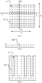
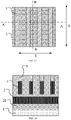
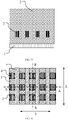
- FIG. 4 is a top perspective view of another exemplary embodiment of the semiconductor structure of the disclosure
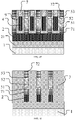
- FIG. 5 is a cross-sectional view along a dotted line A-A in FIG. 1
- FIG. 6 is a cross-sectional view along a dotted line B-B in FIG. 1
- each bit line 2 and the base substrate 1 may be arranged to be insulated from one another through a respective part of the insulator 3.
- a method of forming the first source or drain part 51 and the second source or drain part 53 generally includes that semiconductor material is formed first, and ion doping is performed on both sides of the semiconductor material to form the first source or drain part 51 and the second source or drain part 53.
- the doped ion may have an effect on a dielectric constant of the insulating layer on both sides of the semiconductor material.
- the doped ion may increase the dielectric constant of the insulator 3.
- the semiconductor structure may further include a first conductor part 71 and a second conductor part 72.
- the first conductor part 71 may be located between each bit line 2 and the first source or drain part 51; and the second conductor part 72 may be located on one side of the second source or drain part 53 facing away from the base substrate 1. As shown in FIG. 5 , the arrangement may reduce the size of the first source or drain part 51 and the second source or drain part 53 in a laminating direction, so that the ion doping range of the insulator may be reduced.
- the first conductor part 71 may serve as a bit line contact plug and the second conductor part 72 may serve as a capacitor contact plug.
- the exemplary embodiments further provide a manufacturing method of a semiconductor structure.
- the method may form the above semiconductor structure.
- the method may include the following operations.
- a to-be-etched body is formed.
- the to-be-etched body includes a base substrate, an insulator located on one side of the base substrate and multiple bit lines.
- the bit lines are located in the insulator, and the multiple bit lines are distributed at intervals along a first direction and extend along a second direction.
- multiple second grooves which are distributed at intervals along the second direction and extend along the first direction are formed on one side of the insulator facing away from the bit lines.
- a word line and a fourth insulating layer are sequentially formed in each second groove.
- the fourth insulating layer is located on one side of the word line facing away from a bottom of the second groove.
- multiple through holes distributed in an array are formed on one side of the insulator facing away from the base substrate.
- Orthographic projection of each through hole on the base substrate at least partially coincides with the orthographic projection of a respective bit line on the base substrate.
- the through hole extends to a surface of one side of the bit line facing the through hole.
- the orthographic projection of each through hole on the base substrate is located between the orthographic projections of two adjacent word lines on the base substrate.
- the orthographic projection of only one word line on the base substrate is located between the orthographic projections of two adjacent through holes on the base substrate.
- a fifth insulating layer is formed on one side of the word line exposed to the through hole.
- a first source or drain part, an active part and a second source or drain part are formed in each through hole.
- the first source or drain part is located on one side of the bit line
- the active part is located on one side of the first source or drain part facing away from the bit line
- the second source or drain part is located on one side of the active part facing away from the bit line.
- the operation that a to-be-etched body is formed may include the following operations.
- a substrate material layer is formed. Multiple first grooves, which are distributed at intervals along the first direction and extend along the second direction, are formed on one side surface of the substrate material layer.
- a first insulating layer, a bit line and a second insulating layer are formed in the first groove.
- the bit line is located on one side of the first insulating layer facing away from a bottom of the first groove.
- the second insulating layer is located on one side of the bit line facing away from the bottom of the first groove.
- the substrate material layer on one side, facing an opening of the first groove, of a plane of the bottom of the first groove is removed so as to form the remaining substrate material layer into the base substrate, and a third insulating layer is filled at a position of a removed substrate material layer so as to form the third insulating layer, the first insulating layer and the second insulating layer into the insulator.
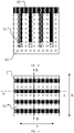
- FIG. 7 is a top view of a semiconductor structure semi-finished product in one exemplary embodiment of a manufacturing method of a semiconductor structure of the disclosure.
- FIG. 8 is a cross-sectional view of a dotted line A-Ain FIG. 7.
- FIG. 9 is a cross-sectional view of a dotted line B-B in FIG. 7 .
- a substrate material layer 01 is formed. Multiple first grooves 11, which are distributed at intervals along the first direction and extend along the second direction, are formed on one side surface of the substrate material layer 01.
- the material of the substrate material layer 01 may be other material, for example, silicon, Silicon-on-Insulator (SOI), germanium, gallium arsenide, and the like.
- Multiple first grooves 11 which are distributed at intervals along the first direction X and extend along the second direction Y are formed on one side of the substrate material layer 01.
- FIG. 10 , FIG. 13 , FIG. 16 , FIG. 19 , FIG. 22 , and FIG. 25 are top views of a semiconductor structure semi-finished product in one exemplary embodiment of a manufacturing method of a semiconductor structure of the disclosure.
- FIG. 11 is a cross-sectional view of a dotted line A-A in FIG. 10 ;
- FIG. 12 is a cross-sectional view of a dotted line B-B in FIG. 10 ;
- FIG. 14 is a cross-sectional view of a dotted line A-A in FIG. 13 ;
- FIG. 15 is a cross-sectional view of a dotted line B-B in FIG. 13 ;
- FIG. 11 is a cross-sectional view of a dotted line A-A in FIG. 10 ;
- FIG. 12 is a cross-sectional view of a dotted line B-B in FIG. 10 ;
- FIG. 14 is a cross-sectional view of a dotted line A-A in FIG. 13
- FIG. 17 is a cross-sectional view of a dotted line A-A in FIG. 16 ;
- FIG. 18 is a cross-sectional view of a dotted line B-B in FIG. 16 ;
- FIG. 20 is a cross-sectional view of a dotted line A-A in FIG. 19 ;
- FIG. 21 is a cross-sectional view of a dotted line B-B in FIG. 19 ;
- FIG. 23 is a cross-sectional view of a dotted line A-A in FIG. 22 ;
- FIG. 24 is a cross-sectional view of a dotted line B-B in FIG. 22 ;
- FIG. 26 is a cross-sectional view of a dotted line A-A in FIG. 25 ; and
- FIG. 27 is a cross-sectional view of a dotted line B-B in FIG. 25 .
- a first insulating layer, a bit line and a second insulating layer are formed in the first groove 11.
- the bit line is located on one side of the first insulating layer facing away from a bottom of the first groove.
- the second insulating layer is located on one side of the first insulating layer facing away from a bottom of the first groove.
- a first insulating material layer 02 may first be deposited through a deposition process on one side, provided with the first groove 11, of the substrate material layer 01 to fill the first groove 11.
- the material of the first insulating material layer 02 may be silicon oxide.
- the first insulating material layer 02 in the first groove 11 may then be partially etched through an etching process to form the first insulating layer 21 in the first groove 11.
- An upper surface of the first insulating layer 21 is lower than the upper surface of the first groove 11.
- a bit line material layer 03 may then be coated through the deposition process on one side, provided with the first groove 11, of the substrate material layer 01 to fill the first groove 11.
- the material of the bit line material layer 03 may be metal tungsten.
- the bit line material layer 03 in the first groove 11 may then be partially etched through the etching process to form the bit line 2 in the first groove 11.
- the upper surface of the bit line 2 is lower than the upper surface of the first groove 11.
- a second insulating material layer 04 may first be deposited through the deposition process on one side, provided with the first groove 11, of the substrate material layer 01 to fill the first groove 11.
- the material of the second insulating material layer 04 may be silicon oxide.
- CMP Chemical Mechanical Polishing
- FIG. 28 , and FIG. 31 are top views of a semiconductor structure semi-finished product in one exemplary embodiment of a manufacturing method of a semiconductor structure of the disclosure.
- FIG. 29 is a cross-sectional view of a dotted line A-A in FIG. 28 ;
- FIG. 30 is a cross-sectional view of a dotted line B-B in FIG. 28 ;
- FIG. 32 is a cross-sectional view of a dotted line A-A in FIG. 31 ;
- FIG. 33 is a cross-sectional view of a dotted line B-B in FIG. 31 .
- first, S13 may include that: the substrate material layer on one side, facing an opening of the first groove, of a plane of the bottom of the first groove is removed through the etching process so as to form the remaining substrate material layer into the base substrate 1. As shown in FIG. 31, FIG. 32 and FIG. 33 , then S13 may further includes that: the third insulating layer 05 is filled at a position of a removed substrate material layer through the deposition process to form the third insulating layer 05, the first insulating layer 21, and the second insulating layer 41 into the insulator 3.
- FIG. 34 is a top view of a semiconductor structure semi-finished product in one exemplary embodiment of a manufacturing method of a semiconductor structure of the disclosure
- FIG. 35 is a cross-sectional view of a dotted line A-A in FIG. 34
- FIG. 36 is a cross-sectional view of a dotted line B-B in FIG. 34 .
- multiple second grooves 051 which are distributed at intervals along the second direction Y and extend along the first direction X may be formed through the etching process on one side of the insulator 3 facing way from the bit lines 2.
- FIG. 37 is a top view of a semiconductor structure semi-finished product in one exemplary embodiment of a manufacturing method of a semiconductor structure of the disclosure
- FIG. 38 is a cross-sectional view of a dotted line A-A in FIG. 37
- FIG. 39 is a cross-sectional view of a dotted line B-B in FIG. 37
- the word line 4 and a fourth insulating layer 7 may be sequentially formed in each second groove 051 through the deposition and etching processes.
- the fourth insulating layer 7 is located on one side of the word line 4 facing away from the bottom of the second groove 051.
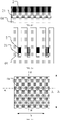
- FIG. 40 is a top perspective view of a semiconductor structure semi-finished product in one exemplary embodiment of a manufacturing method of a semiconductor structure of the disclosure
- FIG. 41 is a cross-sectional view of a dotted line A-A in FIG. 40
- FIG. 42 is a cross-sectional view of a dotted line B-B in FIG. 40
- multiple through holes 8 distributed in an array may be formed on the insulator 3 through the etching process. Orthographic projection of each through hole 8 on the base substrate 1 at least partially coincides with the orthographic projection of a respective bit line 2 on the base substrate 1.
- the through hole 8 extends to a surface of one side, facing the through hole 8, of the bit line 2.
- the orthographic projection of each through hole 8 on the base substrate 1 is located between the orthographic projections of two adjacent word lines 4 on the base substrate 1. Furthermore, in the second direction Y, the orthographic projection of only one word line 4 on the base substrate 1 is located between the orthographic projections of two adjacent through holes 8 on the base substrate 1.
- a fifth insulating layer 9 may be formed through an atomic layer deposition process on one side of the word line 4 exposed to the through hole 8.
- the fifth insulating layer 9 may be used for a gate oxide layer of the word line 4.
- an insulating layer may be deposited on the through hole through the atomic layer deposition process, the insulating layer at the bottom of the through hole is etched, and the insulating layer on a sidewall of the through hole is reserved to form the fifth insulating layer.
- FIG. 43 is a top perspective view of a semiconductor structure semi-finished product in one exemplary embodiment of a manufacturing method of a semiconductor structure of the disclosure
- FIG. 44 is a cross-sectional view of a dotted line A-A in FIG. 43
- FIG. 45 is a cross-sectional view of a dotted line B-B in FIG. 43 .
- S6 a first source or drain part 51, an active part 52, and a second source or drain part 53 are formed in each through hole 8.
- the first source or drain part 51 is located on one side of the bit line 2 facing away from the base substrate 1
- the active part 52 is located on one side of the first source or drain part 51 facing away from the bit line 2
- the second source or drain part 53 is located on one side of the active part 52 facing away from the bit line 2.
- the operation that a first source or drain part 51, an active part 52, and a second source or drain part 53 are formed in each through hole 8 may include that: the through hole 8 is filled with a semiconductor material, and both sides of the semiconductor in the through hole 8 along an extension direction of the through hole 8 are doped to form the first source or drain part 51 and the second source or drain part 53 respectively.
- the semiconductor material may be polysilicon, and the first source or drain part 51 and the second source or drain part 53 are formed through N-type doping or P-type doping.
- a doping ion may be a boron ion, a bismuth ion, a germanium ion, a cobalt ion, a phosphorus ion, and the like.
- the active part may also be doped lightly to adjust a resistance value of the active part.
- the orthographic projection of the active part 52 in a plane of the word line 4 may be on the word line 4.
- the first source or drain part 51 and the second source or drain part 53 may form a source or drain of a switch transistor in a memory cell
- the active part 52 may form the active part of the switch transistor
- a part of the word line 4 may form a gate of the switch transistor
- the fifth insulating layer 9 may form a gate insulating layer of the switch transistor.
- FIG. 46 is a top perspective view of a semiconductor structure semi-finished product in one exemplary embodiment of a manufacturing method of a semiconductor structure of the disclosure
- FIG. 47 is a cross-sectional view of a dotted line A-A in FIG. 46
- FIG. 48 is a cross-sectional view of a dotted line B-B in FIG. 46 .
- the method may further include that: a first conductor part 71 is formed in the through hole 8, the first conductor part 71 being located between each bit line 2 and the first source or drain part 51.
- the method may further include that: a second conductor part 72 is formed in the through hole 8, the second conductor part 72 is located at one side of the second source or drain part 53 facing away from the base substrate 1.
- the material of the first conductor part 71 and the second conductor part 72 may be conductive polysilicon or metal silicide.
- the exemplary embodiments further provide a control method of a semiconductor structure.
- the method is configured to control the semiconductor structure and includes the following operation.
- a turn-on signal is simultaneously input to two adjacent word lines to turn on an active body located between the two word lines, so that capacitance thereof is accessed.
- a PN junction clamped in a middle active body source drain region is inverted to form a passage so as to be turned on, while the PN junction in a side active body source drain region cannot be inverted and cannot form a complete passage due to insufficient gate voltage, so that two word lines and one bit line correspond to one capacitor to achieve the purpose of addressing.
Landscapes
- Engineering & Computer Science (AREA)
- Manufacturing & Machinery (AREA)
- Microelectronics & Electronic Packaging (AREA)
- Computer Hardware Design (AREA)
- Semiconductor Memories (AREA)
Applications Claiming Priority (2)
| Application Number | Priority Date | Filing Date | Title |
|---|---|---|---|
| CN202010921763.5A CN114141772B (zh) | 2020-09-04 | 2020-09-04 | 半导体结构及其制作方法、控制方法 |
| PCT/CN2021/097909 WO2022048217A1 (fr) | 2020-09-04 | 2021-06-02 | Structure semi-conductrice, et son procédé de fabrication et son procédé de commande |
Publications (3)
| Publication Number | Publication Date |
|---|---|
| EP3985672A1 true EP3985672A1 (fr) | 2022-04-20 |
| EP3985672A4 EP3985672A4 (fr) | 2022-06-08 |
| EP3985672B1 EP3985672B1 (fr) | 2024-01-24 |
Family
ID=80470963
Family Applications (1)
| Application Number | Title | Priority Date | Filing Date |
|---|---|---|---|
| EP21773442.5A Active EP3985672B1 (fr) | 2020-09-04 | 2021-06-02 | Structure semi-conductrice, et son procédé de fabrication et son procédé de commande |
Country Status (2)
| Country | Link |
|---|---|
| US (1) | US11871554B2 (fr) |
| EP (1) | EP3985672B1 (fr) |
Families Citing this family (2)
| Publication number | Priority date | Publication date | Assignee | Title |
|---|---|---|---|---|
| KR20230165456A (ko) * | 2022-05-27 | 2023-12-05 | 삼성전자주식회사 | 반도체 장치 및 그 제조 방법 |
| CN116234309B (zh) * | 2022-08-18 | 2024-02-20 | 北京超弦存储器研究院 | 存储器 |
Family Cites Families (17)
| Publication number | Priority date | Publication date | Assignee | Title |
|---|---|---|---|---|
| US6531727B2 (en) * | 2001-02-09 | 2003-03-11 | Micron Technology, Inc. | Open bit line DRAM with ultra thin body transistors |
| US7359226B2 (en) * | 2006-08-28 | 2008-04-15 | Qimonda Ag | Transistor, memory cell array and method for forming and operating a memory device |
| JP5388814B2 (ja) * | 2009-11-24 | 2014-01-15 | 株式会社東芝 | 半導体記憶装置 |
| US7948027B1 (en) | 2009-12-10 | 2011-05-24 | Nanya Technology Corp. | Embedded bit line structure, field effect transistor structure with the same and method of fabricating the same |
| JP5396544B2 (ja) * | 2010-09-08 | 2014-01-22 | 株式会社日立製作所 | 半導体記憶装置 |
| CN102637692B (zh) | 2011-02-10 | 2014-08-20 | 旺宏电子股份有限公司 | 快闪存储器结构及其制造与操作方法 |
| JP5386528B2 (ja) * | 2011-02-21 | 2014-01-15 | 株式会社日立製作所 | 半導体記憶装置およびその製造方法 |
| KR20130027155A (ko) * | 2011-09-07 | 2013-03-15 | 삼성전자주식회사 | 반도체 기억 소자 |
| KR20130075348A (ko) * | 2011-12-27 | 2013-07-05 | 에스케이하이닉스 주식회사 | 매립비트라인을 구비한 반도체장치 및 그 제조 방법 |
| KR20140012864A (ko) * | 2012-07-23 | 2014-02-04 | 에스케이하이닉스 주식회사 | 반도체 소자 및 그 제조 방법 |
| US20150318295A1 (en) * | 2014-04-30 | 2015-11-05 | SanDisk Technologies, Inc. | Vertical floating gate nand with offset dual control gates |
| KR102549609B1 (ko) * | 2016-09-08 | 2023-06-30 | 삼성전자주식회사 | 수직 채널 트랜지스터를 포함하는 반도체 소자 |
| CN107093604A (zh) | 2017-04-27 | 2017-08-25 | 睿力集成电路有限公司 | 动态随机存取存储器及其制造方法 |
| US20200202900A1 (en) * | 2018-12-21 | 2020-06-25 | Applied Materials, Inc. | 3-D DRAM Structure With Vertical Bit-Line |
| US11348932B2 (en) * | 2019-03-06 | 2022-05-31 | Micron Technology, Inc. | Integrated assemblies having transistor body regions coupled to carrier-sink-structures; and methods of forming integrated assemblies |
| KR102713747B1 (ko) * | 2019-07-26 | 2024-10-08 | 에스케이하이닉스 주식회사 | 수직형 메모리 장치 및 수직형 메모리 장치 제조 방법 |
| WO2021056985A1 (fr) * | 2019-09-27 | 2021-04-01 | 福建省晋华集成电路有限公司 | Structure de contact électrique, combinaison de plaque de masque, procédé de fabrication de fiche de contact et dispositif à semi-conducteur |
-
2021
- 2021-06-02 EP EP21773442.5A patent/EP3985672B1/fr active Active
- 2021-08-02 US US17/391,195 patent/US11871554B2/en active Active
Also Published As
| Publication number | Publication date |
|---|---|
| US20220077158A1 (en) | 2022-03-10 |
| US11871554B2 (en) | 2024-01-09 |
| EP3985672B1 (fr) | 2024-01-24 |
| EP3985672A4 (fr) | 2022-06-08 |
Similar Documents
| Publication | Publication Date | Title |
|---|---|---|
| US12127394B2 (en) | Semiconductor devices having buried gates | |
| CN113192968B (zh) | 三维存储器件 | |
| CN112086455B (zh) | 半导体器件及其制造方法 | |
| KR101645257B1 (ko) | 수직 채널 트랜지스터를 구비한 반도체 소자 | |
| US8558306B2 (en) | Semiconductor device and method of manufacturing the same | |
| US8497174B2 (en) | Method of fabricating semiconductor device including vertical channel transistor | |
| CN113257826A (zh) | 半导体存储器件 | |
| US11417675B2 (en) | Three-dimensional semiconductor memory devices | |
| US20240365553A1 (en) | Three-Dimensional Memory Device with Ferroelectric Material | |
| US11469181B2 (en) | Memory device with air gaps for reducing capacitive coupling | |
| US12513888B2 (en) | Memory device and manufacturing method thereof | |
| KR20260011764A (ko) | 반도체 구조 및 그 제조 방법, 전자 장비 | |
| CN115274669B (zh) | 存储器件及其制造方法及包括该存储器件的电子设备 | |
| CN113270413A (zh) | 半导体存储器件 | |
| US11871554B2 (en) | Semiconductor structure, and manufacturing method and control method thereof | |
| CN114141772B (zh) | 半导体结构及其制作方法、控制方法 | |
| US11910595B2 (en) | Semiconductor memory device | |
| US12245420B2 (en) | Method for forming semiconductor memory device | |
| CN120302640A (zh) | 半导体装置 | |
| US20250374564A1 (en) | Semiconductor device and methods for forming the same | |
| US20240172426A1 (en) | Semiconductor device | |
| US20250234527A1 (en) | Semiconductor device | |
| KR20260025115A (ko) | 보호 라이너를 포함하는 반도체 장치 | |
| KR20250044608A (ko) | 반도체 메모리 장치 및 이의 제조 방법 | |
| KR20230047969A (ko) | 반도체 장치 및 그 제조 방법 |
Legal Events
| Date | Code | Title | Description |
|---|---|---|---|
| STAA | Information on the status of an ep patent application or granted ep patent |
Free format text: STATUS: UNKNOWN |
|
| STAA | Information on the status of an ep patent application or granted ep patent |
Free format text: STATUS: THE INTERNATIONAL PUBLICATION HAS BEEN MADE |
|
| PUAI | Public reference made under article 153(3) epc to a published international application that has entered the european phase |
Free format text: ORIGINAL CODE: 0009012 |
|
| STAA | Information on the status of an ep patent application or granted ep patent |
Free format text: STATUS: REQUEST FOR EXAMINATION WAS MADE |
|
| 17P | Request for examination filed |
Effective date: 20210930 |
|
| AK | Designated contracting states |
Kind code of ref document: A1 Designated state(s): AL AT BE BG CH CY CZ DE DK EE ES FI FR GB GR HR HU IE IS IT LI LT LU LV MC MK MT NL NO PL PT RO RS SE SI SK SM TR |
|
| REG | Reference to a national code |
Ref country code: DE Ref legal event code: R079 Ipc: H01L0027108000 Ref country code: DE Ref legal event code: R079 Ref document number: 602021008793 Country of ref document: DE Free format text: PREVIOUS MAIN CLASS: G11C0013000000 Ipc: H01L0027108000 |
|
| A4 | Supplementary search report drawn up and despatched |
Effective date: 20220506 |
|
| RIC1 | Information provided on ipc code assigned before grant |
Ipc: H01L 29/78 20060101ALI20220429BHEP Ipc: H01L 29/66 20060101ALI20220429BHEP Ipc: H01L 27/108 20060101AFI20220429BHEP |
|
| STAA | Information on the status of an ep patent application or granted ep patent |
Free format text: STATUS: EXAMINATION IS IN PROGRESS |
|
| 17Q | First examination report despatched |
Effective date: 20230208 |
|
| REG | Reference to a national code |
Ref country code: DE Ref legal event code: R079 Free format text: PREVIOUS MAIN CLASS: H01L0027108000 Ipc: H10B0012000000 Ref document number: 602021008793 Country of ref document: DE |
|
| GRAP | Despatch of communication of intention to grant a patent |
Free format text: ORIGINAL CODE: EPIDOSNIGR1 |
|
| STAA | Information on the status of an ep patent application or granted ep patent |
Free format text: STATUS: GRANT OF PATENT IS INTENDED |
|
| RIC1 | Information provided on ipc code assigned before grant |
Ipc: H01L 29/78 20060101ALI20230719BHEP Ipc: H01L 29/66 20060101ALI20230719BHEP Ipc: H10B 12/00 20230101AFI20230719BHEP |
|
| DAV | Request for validation of the european patent (deleted) | ||
| DAX | Request for extension of the european patent (deleted) | ||
| INTG | Intention to grant announced |
Effective date: 20230822 |
|
| RIN1 | Information on inventor provided before grant (corrected) |
Inventor name: SHI, ZHICHENG Inventor name: CHEN, TAO |
|
| P01 | Opt-out of the competence of the unified patent court (upc) registered |
Effective date: 20230916 |
|
| GRAS | Grant fee paid |
Free format text: ORIGINAL CODE: EPIDOSNIGR3 |
|
| GRAA | (expected) grant |
Free format text: ORIGINAL CODE: 0009210 |
|
| STAA | Information on the status of an ep patent application or granted ep patent |
Free format text: STATUS: THE PATENT HAS BEEN GRANTED |
|
| AK | Designated contracting states |
Kind code of ref document: B1 Designated state(s): AL AT BE BG CH CY CZ DE DK EE ES FI FR GB GR HR HU IE IS IT LI LT LU LV MC MK MT NL NO PL PT RO RS SE SI SK SM TR |
|
| REG | Reference to a national code |
Ref country code: GB Ref legal event code: FG4D |
|
| REG | Reference to a national code |
Ref country code: CH Ref legal event code: EP |
|
| REG | Reference to a national code |
Ref country code: IE Ref legal event code: FG4D |
|
| REG | Reference to a national code |
Ref country code: DE Ref legal event code: R096 Ref document number: 602021008793 Country of ref document: DE |
|
| REG | Reference to a national code |
Ref country code: LT Ref legal event code: MG9D |
|
| REG | Reference to a national code |
Ref country code: NL Ref legal event code: MP Effective date: 20240124 |
|
| PG25 | Lapsed in a contracting state [announced via postgrant information from national office to epo] |
Ref country code: NL Free format text: LAPSE BECAUSE OF FAILURE TO SUBMIT A TRANSLATION OF THE DESCRIPTION OR TO PAY THE FEE WITHIN THE PRESCRIBED TIME-LIMIT Effective date: 20240124 |
|
| PG25 | Lapsed in a contracting state [announced via postgrant information from national office to epo] |
Ref country code: NL Free format text: LAPSE BECAUSE OF FAILURE TO SUBMIT A TRANSLATION OF THE DESCRIPTION OR TO PAY THE FEE WITHIN THE PRESCRIBED TIME-LIMIT Effective date: 20240124 |
|
| PG25 | Lapsed in a contracting state [announced via postgrant information from national office to epo] |
Ref country code: IS Free format text: LAPSE BECAUSE OF FAILURE TO SUBMIT A TRANSLATION OF THE DESCRIPTION OR TO PAY THE FEE WITHIN THE PRESCRIBED TIME-LIMIT Effective date: 20240524 |
|
| PG25 | Lapsed in a contracting state [announced via postgrant information from national office to epo] |
Ref country code: LT Free format text: LAPSE BECAUSE OF FAILURE TO SUBMIT A TRANSLATION OF THE DESCRIPTION OR TO PAY THE FEE WITHIN THE PRESCRIBED TIME-LIMIT Effective date: 20240124 |
|
| PG25 | Lapsed in a contracting state [announced via postgrant information from national office to epo] |
Ref country code: GR Free format text: LAPSE BECAUSE OF FAILURE TO SUBMIT A TRANSLATION OF THE DESCRIPTION OR TO PAY THE FEE WITHIN THE PRESCRIBED TIME-LIMIT Effective date: 20240425 |
|
| REG | Reference to a national code |
Ref country code: AT Ref legal event code: MK05 Ref document number: 1653176 Country of ref document: AT Kind code of ref document: T Effective date: 20240124 |
|
| PG25 | Lapsed in a contracting state [announced via postgrant information from national office to epo] |
Ref country code: RS Free format text: LAPSE BECAUSE OF FAILURE TO SUBMIT A TRANSLATION OF THE DESCRIPTION OR TO PAY THE FEE WITHIN THE PRESCRIBED TIME-LIMIT Effective date: 20240424 Ref country code: HR Free format text: LAPSE BECAUSE OF FAILURE TO SUBMIT A TRANSLATION OF THE DESCRIPTION OR TO PAY THE FEE WITHIN THE PRESCRIBED TIME-LIMIT Effective date: 20240124 |
|
| PG25 | Lapsed in a contracting state [announced via postgrant information from national office to epo] |
Ref country code: ES Free format text: LAPSE BECAUSE OF FAILURE TO SUBMIT A TRANSLATION OF THE DESCRIPTION OR TO PAY THE FEE WITHIN THE PRESCRIBED TIME-LIMIT Effective date: 20240124 |
|
| PG25 | Lapsed in a contracting state [announced via postgrant information from national office to epo] |
Ref country code: AT Free format text: LAPSE BECAUSE OF FAILURE TO SUBMIT A TRANSLATION OF THE DESCRIPTION OR TO PAY THE FEE WITHIN THE PRESCRIBED TIME-LIMIT Effective date: 20240124 |
|
| PG25 | Lapsed in a contracting state [announced via postgrant information from national office to epo] |
Ref country code: RS Free format text: LAPSE BECAUSE OF FAILURE TO SUBMIT A TRANSLATION OF THE DESCRIPTION OR TO PAY THE FEE WITHIN THE PRESCRIBED TIME-LIMIT Effective date: 20240424 Ref country code: NO Free format text: LAPSE BECAUSE OF FAILURE TO SUBMIT A TRANSLATION OF THE DESCRIPTION OR TO PAY THE FEE WITHIN THE PRESCRIBED TIME-LIMIT Effective date: 20240424 Ref country code: LT Free format text: LAPSE BECAUSE OF FAILURE TO SUBMIT A TRANSLATION OF THE DESCRIPTION OR TO PAY THE FEE WITHIN THE PRESCRIBED TIME-LIMIT Effective date: 20240124 Ref country code: IS Free format text: LAPSE BECAUSE OF FAILURE TO SUBMIT A TRANSLATION OF THE DESCRIPTION OR TO PAY THE FEE WITHIN THE PRESCRIBED TIME-LIMIT Effective date: 20240524 Ref country code: HR Free format text: LAPSE BECAUSE OF FAILURE TO SUBMIT A TRANSLATION OF THE DESCRIPTION OR TO PAY THE FEE WITHIN THE PRESCRIBED TIME-LIMIT Effective date: 20240124 Ref country code: GR Free format text: LAPSE BECAUSE OF FAILURE TO SUBMIT A TRANSLATION OF THE DESCRIPTION OR TO PAY THE FEE WITHIN THE PRESCRIBED TIME-LIMIT Effective date: 20240425 Ref country code: FI Free format text: LAPSE BECAUSE OF FAILURE TO SUBMIT A TRANSLATION OF THE DESCRIPTION OR TO PAY THE FEE WITHIN THE PRESCRIBED TIME-LIMIT Effective date: 20240124 Ref country code: ES Free format text: LAPSE BECAUSE OF FAILURE TO SUBMIT A TRANSLATION OF THE DESCRIPTION OR TO PAY THE FEE WITHIN THE PRESCRIBED TIME-LIMIT Effective date: 20240124 Ref country code: BG Free format text: LAPSE BECAUSE OF FAILURE TO SUBMIT A TRANSLATION OF THE DESCRIPTION OR TO PAY THE FEE WITHIN THE PRESCRIBED TIME-LIMIT Effective date: 20240124 Ref country code: AT Free format text: LAPSE BECAUSE OF FAILURE TO SUBMIT A TRANSLATION OF THE DESCRIPTION OR TO PAY THE FEE WITHIN THE PRESCRIBED TIME-LIMIT Effective date: 20240124 |
|
| PG25 | Lapsed in a contracting state [announced via postgrant information from national office to epo] |
Ref country code: PT Free format text: LAPSE BECAUSE OF FAILURE TO SUBMIT A TRANSLATION OF THE DESCRIPTION OR TO PAY THE FEE WITHIN THE PRESCRIBED TIME-LIMIT Effective date: 20240524 Ref country code: PL Free format text: LAPSE BECAUSE OF FAILURE TO SUBMIT A TRANSLATION OF THE DESCRIPTION OR TO PAY THE FEE WITHIN THE PRESCRIBED TIME-LIMIT Effective date: 20240124 |
|
| PG25 | Lapsed in a contracting state [announced via postgrant information from national office to epo] |
Ref country code: SE Free format text: LAPSE BECAUSE OF FAILURE TO SUBMIT A TRANSLATION OF THE DESCRIPTION OR TO PAY THE FEE WITHIN THE PRESCRIBED TIME-LIMIT Effective date: 20240124 Ref country code: PT Free format text: LAPSE BECAUSE OF FAILURE TO SUBMIT A TRANSLATION OF THE DESCRIPTION OR TO PAY THE FEE WITHIN THE PRESCRIBED TIME-LIMIT Effective date: 20240524 Ref country code: PL Free format text: LAPSE BECAUSE OF FAILURE TO SUBMIT A TRANSLATION OF THE DESCRIPTION OR TO PAY THE FEE WITHIN THE PRESCRIBED TIME-LIMIT Effective date: 20240124 Ref country code: LV Free format text: LAPSE BECAUSE OF FAILURE TO SUBMIT A TRANSLATION OF THE DESCRIPTION OR TO PAY THE FEE WITHIN THE PRESCRIBED TIME-LIMIT Effective date: 20240124 |
|
| PG25 | Lapsed in a contracting state [announced via postgrant information from national office to epo] |
Ref country code: DK Free format text: LAPSE BECAUSE OF FAILURE TO SUBMIT A TRANSLATION OF THE DESCRIPTION OR TO PAY THE FEE WITHIN THE PRESCRIBED TIME-LIMIT Effective date: 20240124 |
|
| PG25 | Lapsed in a contracting state [announced via postgrant information from national office to epo] |
Ref country code: SM Free format text: LAPSE BECAUSE OF FAILURE TO SUBMIT A TRANSLATION OF THE DESCRIPTION OR TO PAY THE FEE WITHIN THE PRESCRIBED TIME-LIMIT Effective date: 20240124 |
|
| PG25 | Lapsed in a contracting state [announced via postgrant information from national office to epo] |
Ref country code: CZ Free format text: LAPSE BECAUSE OF FAILURE TO SUBMIT A TRANSLATION OF THE DESCRIPTION OR TO PAY THE FEE WITHIN THE PRESCRIBED TIME-LIMIT Effective date: 20240124 Ref country code: EE Free format text: LAPSE BECAUSE OF FAILURE TO SUBMIT A TRANSLATION OF THE DESCRIPTION OR TO PAY THE FEE WITHIN THE PRESCRIBED TIME-LIMIT Effective date: 20240124 |
|
| REG | Reference to a national code |
Ref country code: DE Ref legal event code: R097 Ref document number: 602021008793 Country of ref document: DE |
|
| PG25 | Lapsed in a contracting state [announced via postgrant information from national office to epo] |
Ref country code: SK Free format text: LAPSE BECAUSE OF FAILURE TO SUBMIT A TRANSLATION OF THE DESCRIPTION OR TO PAY THE FEE WITHIN THE PRESCRIBED TIME-LIMIT Effective date: 20240124 |
|
| PG25 | Lapsed in a contracting state [announced via postgrant information from national office to epo] |
Ref country code: SM Free format text: LAPSE BECAUSE OF FAILURE TO SUBMIT A TRANSLATION OF THE DESCRIPTION OR TO PAY THE FEE WITHIN THE PRESCRIBED TIME-LIMIT Effective date: 20240124 Ref country code: SK Free format text: LAPSE BECAUSE OF FAILURE TO SUBMIT A TRANSLATION OF THE DESCRIPTION OR TO PAY THE FEE WITHIN THE PRESCRIBED TIME-LIMIT Effective date: 20240124 Ref country code: EE Free format text: LAPSE BECAUSE OF FAILURE TO SUBMIT A TRANSLATION OF THE DESCRIPTION OR TO PAY THE FEE WITHIN THE PRESCRIBED TIME-LIMIT Effective date: 20240124 Ref country code: DK Free format text: LAPSE BECAUSE OF FAILURE TO SUBMIT A TRANSLATION OF THE DESCRIPTION OR TO PAY THE FEE WITHIN THE PRESCRIBED TIME-LIMIT Effective date: 20240124 Ref country code: CZ Free format text: LAPSE BECAUSE OF FAILURE TO SUBMIT A TRANSLATION OF THE DESCRIPTION OR TO PAY THE FEE WITHIN THE PRESCRIBED TIME-LIMIT Effective date: 20240124 |
|
| PLBE | No opposition filed within time limit |
Free format text: ORIGINAL CODE: 0009261 |
|
| STAA | Information on the status of an ep patent application or granted ep patent |
Free format text: STATUS: NO OPPOSITION FILED WITHIN TIME LIMIT |
|
| PG25 | Lapsed in a contracting state [announced via postgrant information from national office to epo] |
Ref country code: IT Free format text: LAPSE BECAUSE OF FAILURE TO SUBMIT A TRANSLATION OF THE DESCRIPTION OR TO PAY THE FEE WITHIN THE PRESCRIBED TIME-LIMIT Effective date: 20240124 |
|
| PG25 | Lapsed in a contracting state [announced via postgrant information from national office to epo] |
Ref country code: IT Free format text: LAPSE BECAUSE OF FAILURE TO SUBMIT A TRANSLATION OF THE DESCRIPTION OR TO PAY THE FEE WITHIN THE PRESCRIBED TIME-LIMIT Effective date: 20240124 |
|
| 26N | No opposition filed |
Effective date: 20241025 |
|
| PG25 | Lapsed in a contracting state [announced via postgrant information from national office to epo] |
Ref country code: MC Free format text: LAPSE BECAUSE OF FAILURE TO SUBMIT A TRANSLATION OF THE DESCRIPTION OR TO PAY THE FEE WITHIN THE PRESCRIBED TIME-LIMIT Effective date: 20240124 |
|
| REG | Reference to a national code |
Ref country code: CH Ref legal event code: PL |
|
| PG25 | Lapsed in a contracting state [announced via postgrant information from national office to epo] |
Ref country code: LU Free format text: LAPSE BECAUSE OF NON-PAYMENT OF DUE FEES Effective date: 20240602 |
|
| PG25 | Lapsed in a contracting state [announced via postgrant information from national office to epo] |
Ref country code: IE Free format text: LAPSE BECAUSE OF NON-PAYMENT OF DUE FEES Effective date: 20240602 |
|
| PG25 | Lapsed in a contracting state [announced via postgrant information from national office to epo] |
Ref country code: BE Free format text: LAPSE BECAUSE OF NON-PAYMENT OF DUE FEES Effective date: 20240630 Ref country code: SI Free format text: LAPSE BECAUSE OF FAILURE TO SUBMIT A TRANSLATION OF THE DESCRIPTION OR TO PAY THE FEE WITHIN THE PRESCRIBED TIME-LIMIT Effective date: 20240124 Ref country code: CH Free format text: LAPSE BECAUSE OF NON-PAYMENT OF DUE FEES Effective date: 20240630 |
|
| PG25 | Lapsed in a contracting state [announced via postgrant information from national office to epo] |
Ref country code: FR Free format text: LAPSE BECAUSE OF NON-PAYMENT OF DUE FEES Effective date: 20240630 |
|
| REG | Reference to a national code |
Ref country code: BE Ref legal event code: MM Effective date: 20240630 |
|
| PGFP | Annual fee paid to national office [announced via postgrant information from national office to epo] |
Ref country code: DE Payment date: 20250618 Year of fee payment: 5 |
|
| PG25 | Lapsed in a contracting state [announced via postgrant information from national office to epo] |
Ref country code: CY Free format text: LAPSE BECAUSE OF FAILURE TO SUBMIT A TRANSLATION OF THE DESCRIPTION OR TO PAY THE FEE WITHIN THE PRESCRIBED TIME-LIMIT; INVALID AB INITIO Effective date: 20210602 |
|
| PG25 | Lapsed in a contracting state [announced via postgrant information from national office to epo] |
Ref country code: RO Free format text: LAPSE BECAUSE OF FAILURE TO SUBMIT A TRANSLATION OF THE DESCRIPTION OR TO PAY THE FEE WITHIN THE PRESCRIBED TIME-LIMIT Effective date: 20240124 |
|
| GBPC | Gb: european patent ceased through non-payment of renewal fee |
Effective date: 20250602 |
|
| PG25 | Lapsed in a contracting state [announced via postgrant information from national office to epo] |
Ref country code: HU Free format text: LAPSE BECAUSE OF FAILURE TO SUBMIT A TRANSLATION OF THE DESCRIPTION OR TO PAY THE FEE WITHIN THE PRESCRIBED TIME-LIMIT; INVALID AB INITIO Effective date: 20210602 |
|
| PG25 | Lapsed in a contracting state [announced via postgrant information from national office to epo] |
Ref country code: GB Free format text: LAPSE BECAUSE OF NON-PAYMENT OF DUE FEES Effective date: 20250602 |