EP3992703A1 - Anzeigesubstrat und flüssigkristallanzeigetafel - Google Patents
Anzeigesubstrat und flüssigkristallanzeigetafel Download PDFInfo
- Publication number
- EP3992703A1 EP3992703A1 EP19930192.0A EP19930192A EP3992703A1 EP 3992703 A1 EP3992703 A1 EP 3992703A1 EP 19930192 A EP19930192 A EP 19930192A EP 3992703 A1 EP3992703 A1 EP 3992703A1
- Authority
- EP
- European Patent Office
- Prior art keywords
- common electrode
- substrate
- transparent conductive
- conductive layer
- pixel
- Prior art date
- Legal status (The legal status is an assumption and is not a legal conclusion. Google has not performed a legal analysis and makes no representation as to the accuracy of the status listed.)
- Withdrawn
Links
- 239000000758 substrate Substances 0.000 title claims abstract description 142
- 239000004973 liquid crystal related substance Substances 0.000 title claims abstract description 57
- 239000010409 thin film Substances 0.000 claims abstract description 41
- 238000009413 insulation Methods 0.000 claims abstract description 5
- 239000010410 layer Substances 0.000 claims description 90
- 239000000463 material Substances 0.000 claims description 15
- 239000011159 matrix material Substances 0.000 claims description 9
- 229910052751 metal Inorganic materials 0.000 claims description 6
- 239000002184 metal Substances 0.000 claims description 6
- 239000007787 solid Substances 0.000 claims description 4
- 230000005684 electric field Effects 0.000 description 15
- 238000002834 transmittance Methods 0.000 description 8
- 238000004519 manufacturing process Methods 0.000 description 7
- 238000000034 method Methods 0.000 description 7
- 230000009286 beneficial effect Effects 0.000 description 3
- 230000000694 effects Effects 0.000 description 3
- XLOMVQKBTHCTTD-UHFFFAOYSA-N Zinc monoxide Chemical compound [Zn]=O XLOMVQKBTHCTTD-UHFFFAOYSA-N 0.000 description 2
- 239000011651 chromium Substances 0.000 description 2
- 239000010949 copper Substances 0.000 description 2
- VYZAMTAEIAYCRO-UHFFFAOYSA-N Chromium Chemical compound [Cr] VYZAMTAEIAYCRO-UHFFFAOYSA-N 0.000 description 1
- RYGMFSIKBFXOCR-UHFFFAOYSA-N Copper Chemical compound [Cu] RYGMFSIKBFXOCR-UHFFFAOYSA-N 0.000 description 1
- ZOKXTWBITQBERF-UHFFFAOYSA-N Molybdenum Chemical compound [Mo] ZOKXTWBITQBERF-UHFFFAOYSA-N 0.000 description 1
- 229910000583 Nd alloy Inorganic materials 0.000 description 1
- 229910001080 W alloy Inorganic materials 0.000 description 1
- 230000004075 alteration Effects 0.000 description 1
- 229910052782 aluminium Inorganic materials 0.000 description 1
- XAGFODPZIPBFFR-UHFFFAOYSA-N aluminium Chemical compound [Al] XAGFODPZIPBFFR-UHFFFAOYSA-N 0.000 description 1
- UBSJOWMHLJZVDJ-UHFFFAOYSA-N aluminum neodymium Chemical compound [Al].[Nd] UBSJOWMHLJZVDJ-UHFFFAOYSA-N 0.000 description 1
- 229910052804 chromium Inorganic materials 0.000 description 1
- 239000002131 composite material Substances 0.000 description 1
- 229910052802 copper Inorganic materials 0.000 description 1
- 230000014509 gene expression Effects 0.000 description 1
- 239000011521 glass Substances 0.000 description 1
- AMGQUBHHOARCQH-UHFFFAOYSA-N indium;oxotin Chemical compound [In].[Sn]=O AMGQUBHHOARCQH-UHFFFAOYSA-N 0.000 description 1
- 239000007769 metal material Substances 0.000 description 1
- 239000000203 mixture Substances 0.000 description 1
- 229910052750 molybdenum Inorganic materials 0.000 description 1
- 239000011733 molybdenum Substances 0.000 description 1
- MGRWKWACZDFZJT-UHFFFAOYSA-N molybdenum tungsten Chemical compound [Mo].[W] MGRWKWACZDFZJT-UHFFFAOYSA-N 0.000 description 1
- 230000003071 parasitic effect Effects 0.000 description 1
- 230000005855 radiation Effects 0.000 description 1
- 239000011347 resin Substances 0.000 description 1
- 229920005989 resin Polymers 0.000 description 1
- 239000002356 single layer Substances 0.000 description 1
- XLYOFNOQVPJJNP-UHFFFAOYSA-N water Substances O XLYOFNOQVPJJNP-UHFFFAOYSA-N 0.000 description 1
- 239000011787 zinc oxide Substances 0.000 description 1
Images


Classifications
-
- G—PHYSICS
- G02—OPTICS
- G02F—OPTICAL DEVICES OR ARRANGEMENTS FOR THE CONTROL OF LIGHT BY MODIFICATION OF THE OPTICAL PROPERTIES OF THE MEDIA OF THE ELEMENTS INVOLVED THEREIN; NON-LINEAR OPTICS; FREQUENCY-CHANGING OF LIGHT; OPTICAL LOGIC ELEMENTS; OPTICAL ANALOGUE/DIGITAL CONVERTERS
- G02F1/00—Devices or arrangements for the control of the intensity, colour, phase, polarisation or direction of light arriving from an independent light source, e.g. switching, gating or modulating; Non-linear optics
- G02F1/01—Devices or arrangements for the control of the intensity, colour, phase, polarisation or direction of light arriving from an independent light source, e.g. switching, gating or modulating; Non-linear optics for the control of the intensity, phase, polarisation or colour
- G02F1/13—Devices or arrangements for the control of the intensity, colour, phase, polarisation or direction of light arriving from an independent light source, e.g. switching, gating or modulating; Non-linear optics for the control of the intensity, phase, polarisation or colour based on liquid crystals, e.g. single liquid crystal display cells
- G02F1/133—Constructional arrangements; Operation of liquid crystal cells; Circuit arrangements
- G02F1/136—Liquid crystal cells structurally associated with a semi-conducting layer or substrate, e.g. cells forming part of an integrated circuit
- G02F1/1362—Active matrix addressed cells
- G02F1/136286—Wiring, e.g. gate line, drain line
-
- G—PHYSICS
- G02—OPTICS
- G02F—OPTICAL DEVICES OR ARRANGEMENTS FOR THE CONTROL OF LIGHT BY MODIFICATION OF THE OPTICAL PROPERTIES OF THE MEDIA OF THE ELEMENTS INVOLVED THEREIN; NON-LINEAR OPTICS; FREQUENCY-CHANGING OF LIGHT; OPTICAL LOGIC ELEMENTS; OPTICAL ANALOGUE/DIGITAL CONVERTERS
- G02F1/00—Devices or arrangements for the control of the intensity, colour, phase, polarisation or direction of light arriving from an independent light source, e.g. switching, gating or modulating; Non-linear optics
- G02F1/01—Devices or arrangements for the control of the intensity, colour, phase, polarisation or direction of light arriving from an independent light source, e.g. switching, gating or modulating; Non-linear optics for the control of the intensity, phase, polarisation or colour
- G02F1/13—Devices or arrangements for the control of the intensity, colour, phase, polarisation or direction of light arriving from an independent light source, e.g. switching, gating or modulating; Non-linear optics for the control of the intensity, phase, polarisation or colour based on liquid crystals, e.g. single liquid crystal display cells
- G02F1/133—Constructional arrangements; Operation of liquid crystal cells; Circuit arrangements
- G02F1/1333—Constructional arrangements; Manufacturing methods
- G02F1/1343—Electrodes
- G02F1/134309—Electrodes characterised by their geometrical arrangement
- G02F1/134372—Electrodes characterised by their geometrical arrangement for fringe field switching [FFS] where the common electrode is not patterned
-
- G—PHYSICS
- G02—OPTICS
- G02F—OPTICAL DEVICES OR ARRANGEMENTS FOR THE CONTROL OF LIGHT BY MODIFICATION OF THE OPTICAL PROPERTIES OF THE MEDIA OF THE ELEMENTS INVOLVED THEREIN; NON-LINEAR OPTICS; FREQUENCY-CHANGING OF LIGHT; OPTICAL LOGIC ELEMENTS; OPTICAL ANALOGUE/DIGITAL CONVERTERS
- G02F1/00—Devices or arrangements for the control of the intensity, colour, phase, polarisation or direction of light arriving from an independent light source, e.g. switching, gating or modulating; Non-linear optics
- G02F1/01—Devices or arrangements for the control of the intensity, colour, phase, polarisation or direction of light arriving from an independent light source, e.g. switching, gating or modulating; Non-linear optics for the control of the intensity, phase, polarisation or colour
- G02F1/13—Devices or arrangements for the control of the intensity, colour, phase, polarisation or direction of light arriving from an independent light source, e.g. switching, gating or modulating; Non-linear optics for the control of the intensity, phase, polarisation or colour based on liquid crystals, e.g. single liquid crystal display cells
- G02F1/133—Constructional arrangements; Operation of liquid crystal cells; Circuit arrangements
- G02F1/136—Liquid crystal cells structurally associated with a semi-conducting layer or substrate, e.g. cells forming part of an integrated circuit
- G02F1/1362—Active matrix addressed cells
- G02F1/136209—Light shielding layers, e.g. black matrix, incorporated in the active matrix substrate, e.g. structurally associated with the switching element
-
- G—PHYSICS
- G02—OPTICS
- G02F—OPTICAL DEVICES OR ARRANGEMENTS FOR THE CONTROL OF LIGHT BY MODIFICATION OF THE OPTICAL PROPERTIES OF THE MEDIA OF THE ELEMENTS INVOLVED THEREIN; NON-LINEAR OPTICS; FREQUENCY-CHANGING OF LIGHT; OPTICAL LOGIC ELEMENTS; OPTICAL ANALOGUE/DIGITAL CONVERTERS
- G02F1/00—Devices or arrangements for the control of the intensity, colour, phase, polarisation or direction of light arriving from an independent light source, e.g. switching, gating or modulating; Non-linear optics
- G02F1/01—Devices or arrangements for the control of the intensity, colour, phase, polarisation or direction of light arriving from an independent light source, e.g. switching, gating or modulating; Non-linear optics for the control of the intensity, phase, polarisation or colour
- G02F1/13—Devices or arrangements for the control of the intensity, colour, phase, polarisation or direction of light arriving from an independent light source, e.g. switching, gating or modulating; Non-linear optics for the control of the intensity, phase, polarisation or colour based on liquid crystals, e.g. single liquid crystal display cells
- G02F1/133—Constructional arrangements; Operation of liquid crystal cells; Circuit arrangements
- G02F1/136—Liquid crystal cells structurally associated with a semi-conducting layer or substrate, e.g. cells forming part of an integrated circuit
- G02F1/1362—Active matrix addressed cells
- G02F1/136218—Shield electrodes
-
- G—PHYSICS
- G02—OPTICS
- G02F—OPTICAL DEVICES OR ARRANGEMENTS FOR THE CONTROL OF LIGHT BY MODIFICATION OF THE OPTICAL PROPERTIES OF THE MEDIA OF THE ELEMENTS INVOLVED THEREIN; NON-LINEAR OPTICS; FREQUENCY-CHANGING OF LIGHT; OPTICAL LOGIC ELEMENTS; OPTICAL ANALOGUE/DIGITAL CONVERTERS
- G02F1/00—Devices or arrangements for the control of the intensity, colour, phase, polarisation or direction of light arriving from an independent light source, e.g. switching, gating or modulating; Non-linear optics
- G02F1/01—Devices or arrangements for the control of the intensity, colour, phase, polarisation or direction of light arriving from an independent light source, e.g. switching, gating or modulating; Non-linear optics for the control of the intensity, phase, polarisation or colour
- G02F1/13—Devices or arrangements for the control of the intensity, colour, phase, polarisation or direction of light arriving from an independent light source, e.g. switching, gating or modulating; Non-linear optics for the control of the intensity, phase, polarisation or colour based on liquid crystals, e.g. single liquid crystal display cells
- G02F1/133—Constructional arrangements; Operation of liquid crystal cells; Circuit arrangements
- G02F1/136—Liquid crystal cells structurally associated with a semi-conducting layer or substrate, e.g. cells forming part of an integrated circuit
- G02F1/1362—Active matrix addressed cells
- G02F1/1368—Active matrix addressed cells in which the switching element is a three-electrode device
-
- G—PHYSICS
- G02—OPTICS
- G02F—OPTICAL DEVICES OR ARRANGEMENTS FOR THE CONTROL OF LIGHT BY MODIFICATION OF THE OPTICAL PROPERTIES OF THE MEDIA OF THE ELEMENTS INVOLVED THEREIN; NON-LINEAR OPTICS; FREQUENCY-CHANGING OF LIGHT; OPTICAL LOGIC ELEMENTS; OPTICAL ANALOGUE/DIGITAL CONVERTERS
- G02F2201/00—Constructional arrangements not provided for in groups G02F1/00 - G02F7/00
- G02F2201/12—Constructional arrangements not provided for in groups G02F1/00 - G02F7/00 electrode
- G02F2201/121—Constructional arrangements not provided for in groups G02F1/00 - G02F7/00 electrode common or background
Definitions
- the present disclosure relates to the field of display technology, and particularly to a display substrate and a liquid crystal panel.
- liquid crystal display devices occupy a dominant position in the product market due to their characteristics of small size, low power consumption, relatively low manufacturing cost, no radiation and so on. It has always been an important issue for those skilled in the art how to improve the light leakage among pixels of a liquid crystal display device and thereby improve the display quality.
- a display substrate including:
- the common electrode further includes a first common electrode line connected to the transparent conductive layer; a material of the first common electrode line is a light-shielding metal, and the orthographic projection of the gap, which is between two pixel electrodes adjacent in the column direction of the pixel electrode group, on the substrate falls within an orthographic projection of the first common electrode line on the substrate.
- an electrical conductivity of the first common electrode line is greater than the electrical conductivity of the transparent conductive layer.
- a line width c of the first common electrode line and the gap b between two pixel electrodes adjacent in the column direction of the pixel electrode group satisfy a relationship of 2 micrometers ⁇ c - b ⁇ 5 micrometers.
- the first common electrode line and the transparent conductive layer are stacked on each other; or the first common electrode line is connected to the transparent conductive layer by a via structure.
- the first common electrode line is located on a side of the transparent conductive layer away from the substrate; or the first common electrode line is located on a side of the transparent conductive layer close to the substrate side.
- the pixel electrodes are located on a side of the transparent conductive layer away from the substrate, wherein the transparent conductive layer includes a plurality of common electrode units which are arranged apart from and connected to each other, the common electrode unit has a planar structure, the pixel electrode has a slit structure, and an orthographic projection of the pixel electrode on the substrate falls within an orthographic projection of the common electrode unit on the substrate.
- the first common electrode line is located on a side of the transparent conductive layer away from the substrate and is stacked on the transparent conductive layer, wherein the first common electrode line is formed in the same layer as the gate lines.
- an orthographic projection of every two pixel electrodes adjacent in the column direction of the pixel electrode group on the substrate falls within an orthographic projection of one of the common electrode units on the substrate.
- At least two common electrode units adjacent in the column direction are connected by a jumper.
- the jumper is formed in the same layer as the pixel electrode, and the jumper is connected to the common electrode unit through a via structure.
- the transparent conductive layer is located on a side of the pixel electrode away from the substrate, wherein the pixel electrode has a planar structure, and the transparent conductive layer has a slit structure; the orthographic projection of the gap, which is between two pixel electrodes adjacent in the column direction of the pixel electrode group, on the substrate falls within an orthographic projection of a solid portion of the transparent conductive layer on the substrate.
- the common electrode further includes second common electrode lines respectively disposed on opposite sides of two rows of pixel electrodes of the pixel electrode group, wherein the second common electrode lines are connected to the transparent conductive layer.
- the common electrode further includes a third common electrode line disposed between two rows of pixel electrodes of the pixel electrode group, wherein the third common electrode line is connected to the transparent conductive layer.
- two pixel electrodes located in different pixel electrode groups and adjacent in the column direction are respectively connected to sources of the thin film transistors, and drains of the respectively connected thin film transistors are connected as an integrated structure by a connection portion.
- a gate of the thin film transistor is a part of the gate line, and an orthographic projection of the connection portion on the substrate does not overlap with an orthographic projection of the gate line on the substrate.
- the drain of the thin film transistor is U-shaped, and the source of the thin film transistor extends into the U-shaped opening and is spaced apart from the drain; the U-shaped openings of the drains of the thin film transistors, to which two pixel electrodes located in different pixel electrode groups and adjacent in the column direction are respectively connected, are in opposite directions and connected at the bottom.
- a liquid crystal panel including the display substrate according to any one of the foregoing technical solutions.
- the liquid crystal panel further includes a light-shielding matrix having a plurality of light-transmitting regions, wherein an orthographic projection of every two pixel electrodes adjacent in the column direction of the pixel electrode group on the substrate falls within an orthographic projection of one of the light-transmitting regions on the substrate.
- first, second or the like in the present disclosure does not denote any order, quantity or importance, but are merely used to distinguish between different components.
- a word such as “includes” or “comprises” means that the element before the word covers the elements listed after the word, without excluding the possibility of also covering other elements.
- the terms “up”, “down” and the like are used only to represent a relative positional relationship, and the relative positional relationship may be changed if the absolute position of the described object changes.
- a specific component when it is described that a specific component is disposed between a first component and a second component, there may be an intervening component between the specific component and the first component or the second component, or there may be no intervening component therebetween.
- the specific component When it is described that a specific component is connected to other components, the specific component may be directly connected to the other components without an intervening component, or there may be an intervening component without being directly connected with the other components.
- the liquid crystal display device includes a liquid crystal panel and a backlight module located on the back side of the liquid crystal panel.
- the liquid crystal panel itself does not emit light. In order to display, it is needed for the backlight module to provide backlight. Therefore, the transmittance of the liquid crystal panel is a critical factor affecting the display quality of the liquid crystal display device.
- the liquid crystal panel generally includes a display substrate and a counter substrate disposed apart from each other, and a liquid crystal layer located between the display substrate and the counter substrate.
- Pixel electrodes of the display substrate are disposed in one-to-one correspondence to the sub-pixels of the liquid crystal panel.
- a thin film transistor When a thin film transistor is turned on, a data voltage signal is transmitted on a data line to the pixel electrodes through the thin film transistor. Since a common electrode layer has an equal potential as a whole, a voltage difference is generated between the pixel electrodes and the common electrode, forming an electric field accordingly.
- the electric field formed by the pixel electrodes and the common electrode controls the deflection of liquid crystal molecules, thereby achieving grayscale display of the sub-pixels of the liquid crystal panel.
- a lateral electric field is also formed at the gap between adjacent pixel electrodes due to the difference in potential therebetween.
- This lateral electric field affects the deflection of nearby liquid crystal molecules, causing light leakage between the sub-pixels of the liquid crystal panel.
- the light leakage is generally blocked by a light-shielding matrix provided on the liquid crystal panel, which affects the aperture ratio of the sub-pixel to a certain extent, and further affects the transmittance of the liquid crystal panel.
- the aperture ratio refers to the ratio of the light-transmitting region of the sub-pixel to the area of the sub-pixel.
- embodiments of the present disclosure provide a display substrate, a liquid crystal panel, and a liquid crystal display device to increase the aperture ratio of the sub-pixel, thereby improving the transmittance of the liquid crystal panel, and improving the display quality of the liquid crystal display device.
- a row direction refers to the horizontal arrangement direction of an array
- a column direction refers to the longitudinal arrangement direction of the array.
- the row and column directions are determined relative to one of the use states of the liquid crystal display device, and should not be understood as absolute horizontal and vertical directions.
- connection refers to an electrical connection.
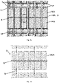
- a display substrate includes: a substrate 1; and a common electrode 2 and a pixel electrode array layer 3 which are located on a side of the substrate 1 and are spaced by insulation, wherein,
- the specific material of the substrate 1 is not limited, and materials such as glass or transparent resin may be used.
- the specific materials of the transparent conductive layer 4 and the pixel electrode array layer 3 are not limited, and for example, materials such as indium tin oxide or zinc oxide may be used.
- the common electrode 2 and the pixel electrode array layer 3 are spaced by insulation via an insulating layer 6.
- the display substrate further includes a data line 13 extending along the column direction and provided on a side of the column of the pixel electrodes.
- a portion of the gate line 10 serves as a gate 9 of the thin film transistor
- a drain 12 of the thin film transistor is connected to the data line 13
- a source 11 of the thin film transistor is connected to the pixel electrode 5.
- the source and the drain as two electrodes of the thin film transistor are only relative terms. Therefore, it is also possible that the source of the thin film transistor may be connected to the data line 13 and the drain of the thin film transistor may be connected to the pixel electrode 5.
- two gate lines 10 are provided between two adjacent pixel electrode groups, and no gate line is provided between two rows of pixel electrodes 5 of the same pixel electrode group.
- One of the two gate lines 10 is connected to the gates of the thin film transistors 7 corresponding to an upper row of pixel electrodes 5, and the other is connected to the gates of the thin film transistors 7 corresponding to a lower row of pixel electrodes 5.
- the thin film transistors and the gate lines connected thereto are provided between two adjacent pixel electrode groups, and no thin film transistors and gate lines are provided between the two rows of pixel electrodes of the same pixel electrode group.
- the structure of the thin film transistors and the gate lines on the display substrate may be designed to be more compact, thereby reducing the occupied area on the display substrate.
- the area of the light-shielding portion thereof may be also reduced accordingly. Therefore, by adopting the technical solution of the above embodiment of the present disclosure, it is possible to increase the area of the light-transmitting region of the sub-pixel, thereby improving the aperture ratio of the sub-pixel.
- the pixel electrodes 5 are located on a side of the transparent conductive layer 4 away from the substrate 1, wherein the transparent conductive layer 4 includes a plurality of common electrode units 14 which are arranged apart from and connected to each other, the common electrode unit 14 has a planar structure, the pixel electrode 5 has a slit structure, and an orthographic projection of the pixel electrode 5 on the substrate 1 falls within an orthographic projection of the common electrode unit 14 on the substrate 1.
- an electric field is generated at the edge of the slit structure of the pixel electrodes 5, and an electric field is also generated between the pixel electrodes 5 and the common electrode units 14, thereby forming a multi-dimensional electric field.
- the multi-dimensional electric field can deflect most liquid crystal molecules of the liquid crystal layer, thereby improving the working efficiency and the transmittance of the liquid crystal panel.
- the liquid crystal display device adopting this display substrate has better picture quality, and has the characteristics of high resolution, high transmittance, low power consumption, wide viewing angle, high aperture ratio, low chromatic aberration, and no squeeze water ripple effect.
- the orthographic projection of every two pixel electrodes adjacent in the column direction of the pixel electrode group on the substrate 1 falls within the orthographic projection of one of the common electrode units 14 on the substrate 1. That is, one of the common electrode units 14 is disposed corresponding to two pixel electrodes 5 adjacent in the column direction of the same pixel electrode group. At least two common electrode units 14 adjacent in the column direction are connected by a jumper 15 so that each common electrode unit 14 has an equal potential.
- the jumper 15 is formed in the same layer as the pixel electrode 5, and the jumper 15 is connected to the common electrode unit 14 through a via structure. In other embodiments, the jumper 15 may also be formed in the same layer as the common electrode unit.
- the common electrode 2 further includes a first common electrode line 8 connected to the transparent conductive layer 4; the material of the first common electrode line 8 is light-shielding metal, and the orthographic projection of the gap, which is between two pixel electrodes 5 adjacent in the column direction of the pixel electrode group, on the substrate 1 falls within the orthographic projection of the first common electrode line 8 on the substrate 1.
- the first common electrode line 8 is disposed between two rows of pixel electrodes 5 of the pixel electrode group and extends along the row direction, which is used to transmit a common voltage signal to the transparent conductive layer 4 more uniformly, thereby reducing the in-plane voltage drop of the transparent conductive layer 4.
- the first common electrode line 8 is located on a side of the transparent conductive layer 4 away from the substrate 1 and is stacked on the transparent conductive layer 4, so that the first common electrode line 8 may be formed in the same layer as the gate lines 10 described above, which makes the manufacturing process of the display substrate easier, and the manufacturing cost is lower.
- the specific location of the first common electrode line is not limited to that shown in FIG. 1c .
- the first common electrode line may also be located on a side of the transparent conductive layer close to the substrate.
- the first common electrode line and the transparent conductive layer may also be connected by a via structure.
- the material of the first common electrode line 8 is a light-shielding metal, and the orthographic projection of the gap, which is between two pixel electrodes 5 adjacent in the column direction of the pixel electrode group, on the substrate 1 falls within the orthographic projection of the first common electrode line 8 on the substrate 1, the first common electrode line 8 may shield the backlight from the back side of the display substrate, thereby effectively avoiding the light leakage at the gap.
- a line width c of the first common electrode line 8 and the gap b between two pixel electrodes 5 adjacent in the column direction of a pixel electrode group satisfy a relationship of 2 micrometers ⁇ c - b ⁇ 5 micrometers.
- the first common electrode line 8 has a better shielding effect, and has less influence on the aperture ratio of the sub-pixel. It is relatively easy to control the manufacturing accuracy, and it is beneficial to reducing the manufacturing cost.
- the electrical conductivity of the first common electrode line 8 is greater than the electrical conductivity of the transparent conductive layer 4.
- the first common electrode line 8 is connected to the transparent conductive layer 4, which is equivalent to the parallel connection of the first common electrode line 8 and the transparent conductive layer 4, thereby significantly reducing the resistance of the common electrode 2, being beneficial to improve the display delay of the liquid crystal display device, and improving the picture quality.
- the specific material of the first common electrode line 8 for example, a single-layer structure of aluminum neodymium alloy (AINd), aluminum (Al), copper (Cu), molybdenum (Mo), molybdenum-tungsten alloy (MoW), or chromium (Cr) may be used. A composite layer structure composed of any combination of these metal materials may also be used.
- the first common electrode line 8 and the gate lines 10 are made of the same material and are formed in the same layer, which does not increase the process flow and the manufacturing cost of the display substrate.
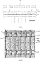
- the transparent conductive layer 4 is located on a side of the pixel electrode 5 away from the substrate 1, wherein the pixel electrode 5 has a planar structure, and the transparent conductive layer 4 has a slit structure, an orthographic projection of a gap, which is between two pixel electrodes 5 adjacent in the column direction of a pixel electrode group, on the substrate 1 falls within an orthographic projection of a solid part of the transparent conductive layer 4 on the substrate 1.
- an electric field is generated at the edge of the slit structure of the transparent conductive layer 4, and an electric field is also generated between the pixel electrode 5 and the transparent conductive layer 4, thereby forming a multi-dimensional electric field, which may improve the working efficiency and the transmittance of the liquid crystal panel, thereby improving the display quality of the liquid crystal display device.
- the transparent conductive layer 4 Since the transparent conductive layer 4 is located on a side of the pixel electrode 5 away from the substrate 1, and the orthographic projection of the gap, which is between two pixel electrodes 5 adjacent in the column direction of the pixel electrode group, on the substrate 1 falls within the orthographic projection of the solid part of the transparent conductive layer 4 on the substrate 1, when the liquid crystal panel including this display substrate is in operation, the lateral electric field at the gap described above cannot pass through the transparent conductive layer 4 to affect the deflection of the liquid crystal molecules. In other words, the transparent conductive layer 4 has a shielding effect on the lateral electric field at the gap described above, thereby avoiding the lateral electric field from affecting the deflection of nearby liquid crystal molecules, and effectively improving the light leakage phenomenon.
- the common electrode 2 in addition to the transparent conductive layer 4, the common electrode 2 further includes second common electrode lines 16 respectively disposed on the opposite sides of two rows of pixel electrodes 5 of the pixel electrode group, wherein the second common electrode lines 16 are connected to the transparent conductive layer 4.
- the common electrode 2 may further include a third common electrode line 22 disposed between two rows of pixel electrodes 5 of the pixel electrode group, wherein the third common electrode line 22 is connected to the transparent conductive layer 4.
- the second common electrode lines 16 and the third common electrode line 22 are used to transmit a common voltage signal to the transparent conductive layer 4 more uniformly, thereby reducing the in-plane voltage drop of the transparent conductive layer 4.
- the selection of the material of the second common electrode lines 16 and the third common electrode line 22 may refer to the first common electrode line 8 described above.
- the second common electrode lines 16 are made of the same material and are formed in the same layer as the gate lines 10 described above, which does not increase the process flow and the manufacturing cost of the display substrate.
- the second common electrode lines 16 and the third common electrode line 22 are connected to the transparent conductive layer 4 by via structures. There is no limitation to the number of the via structures, which can be specified according to the actual product.
- the transparent conductive layer 4 is located on a side of the pixel electrode 5 away from the substrate 1, wherein the pixel electrode 5 has a planar structure, and the transparent conductive layer 4 has a slit structure.
- the projection of the gap, which is between two pixel electrodes 5 adjacent in the column direction of the pixel electrode group, on the substrate 1 overlaps with the projection of one of the slits of the transparent conductive layer 4 on the substrate 1, and thus the first common electrode line 8 is designed in order to avoid the light leakage from occurring at the pixel gap.
- the material of the first common electrode line 8 is light-shielding metal, and the orthographic projection of the gap, which is between two pixel electrodes 5 adjacent in the column direction of the pixel electrode group, on the substrate 1 falls within the orthographic projection of the first common electrode line 8 on the substrate 1. Therefore, the first common electrode line 8 may shield the backlight from the back side of the display substrate, thereby effectively avoiding the light leakage at the gap.
- two pixel electrodes 5 located in different pixel electrode groups and adjacent to each other in the column direction on the display substrate are respectively connected to the source electrodes 11 of the thin film transistors 7, and the drain electrodes 12 of the thin film transistors 7 to which these two pixel electrodes 5 are respectively connected are connected as an integrated structure by a connection portion 21.
- the structure design of the display substrate at two adjacent thin film transistors 7 is relatively compact, which is easy to process, and is beneficial to improve the aperture ratio of the sub-pixel.
- the structure of the thin film transistor 7 is designed as follows: the drain electrode 12 is U-shaped, the source electrode 11 extends into the U-shaped opening 17 and is spaced apart from the drain electrode 12; the U-shaped openings of drain electrodes of the thin film transistors 7, to which the two pixel electrodes 5 located in different pixel electrode groups and adjacent to each other in the column direction are respectively connected, are in opposite directions and connected at the bottom.
- the specific shape of the drain electrode 12 for example, it may be designed to be U-shaped.
- the distance e between the portion of the source electrode 11 in the opening 17 of the drain electrode 12 and the bottom of the opening 17 satisfies: 2.2 micrometers ⁇ e ⁇ 2.5 micrometers.
- SSM Single Slit Mask
- the gate electrode 9 of the thin film transistor 7 is a part of the gate line 10, and the orthographic projection of the connection portion 21 on the substrate 1 does not overlap with the orthographic projection of the gate line 10 on the substrate 1. In this way, the parasitic capacitance between the gate line layer and the data line layer may be reduced, thereby reducing the circuit load and reducing the power consumption of the liquid crystal panel.
- an embodiment of the present disclosure also provides a liquid crystal panel 100 including the display substrate 18 of any one of the foregoing embodiments.
- the liquid crystal panel 100 includes a display substrate 18 and a counter substrate 19 which are spaced apart from each other, and a liquid crystal layer 20 between the display substrate 18 and the counter substrate 19.
- the liquid crystal panel 100 includes a light-shielding matrix (not shown in the figure). There is no limitation to the position of the light-shielding matrix. For example, it may be disposed on the display substrate 18 or the counter substrate 19.
- the light-shielding matrix has a plurality of light-transmitting regions.
- the orthographic projection of every two pixel electrodes 5 adjacent in the column direction of the pixel electrode group described above on the substrate 1 falls within the orthographic projection of one of the light-transmitting regions on the substrate 1. That is, every two pixel electrodes 5 adjacent in the column direction are arranged corresponding to one of the light-transmitting regions.
- the transmittance of the liquid crystal panel is high.
- An embodiment of the present disclosure also provides a liquid crystal display device, including the liquid crystal panel of the foregoing embodiment. Since the liquid crystal panel has a high transmittance, the liquid crystal display device has better display quality.
- the type of the liquid crystal display device for example, it may be a display, a tablet computer, a television, an electronic paper, a display screen, and so on.
Landscapes
- Physics & Mathematics (AREA)
- Nonlinear Science (AREA)
- Mathematical Physics (AREA)
- Chemical & Material Sciences (AREA)
- Crystallography & Structural Chemistry (AREA)
- General Physics & Mathematics (AREA)
- Optics & Photonics (AREA)
- Engineering & Computer Science (AREA)
- Microelectronics & Electronic Packaging (AREA)
- Liquid Crystal (AREA)
- Geometry (AREA)
Applications Claiming Priority (1)
| Application Number | Priority Date | Filing Date | Title |
|---|---|---|---|
| PCT/CN2019/093664 WO2020258242A1 (zh) | 2019-06-28 | 2019-06-28 | 显示基板及液晶面板 |
Publications (2)
| Publication Number | Publication Date |
|---|---|
| EP3992703A1 true EP3992703A1 (de) | 2022-05-04 |
| EP3992703A4 EP3992703A4 (de) | 2023-02-01 |
Family
ID=74061450
Family Applications (1)
| Application Number | Title | Priority Date | Filing Date |
|---|---|---|---|
| EP19930192.0A Withdrawn EP3992703A4 (de) | 2019-06-28 | 2019-06-28 | Anzeigesubstrat und flüssigkristallanzeigetafel |
Country Status (4)
| Country | Link |
|---|---|
| US (1) | US20210405488A1 (de) |
| EP (1) | EP3992703A4 (de) |
| CN (1) | CN112689791A (de) |
| WO (1) | WO2020258242A1 (de) |
Families Citing this family (4)
| Publication number | Priority date | Publication date | Assignee | Title |
|---|---|---|---|---|
| CN110543039B (zh) * | 2019-09-10 | 2022-09-02 | 京东方科技集团股份有限公司 | 显示面板和显示装置 |
| CN114994989B (zh) * | 2022-05-25 | 2023-10-27 | 京东方科技集团股份有限公司 | 阵列基板及显示装置 |
| CN114779547B (zh) * | 2022-05-27 | 2023-11-03 | 京东方科技集团股份有限公司 | 一种显示基板及其制备方法、显示装置 |
| WO2025025166A1 (zh) * | 2023-08-02 | 2025-02-06 | 京东方科技集团股份有限公司 | 阵列基板、显示面板和显示装置 |
Family Cites Families (10)
| Publication number | Priority date | Publication date | Assignee | Title |
|---|---|---|---|---|
| TW454101B (en) * | 1995-10-04 | 2001-09-11 | Hitachi Ltd | In-plane field type liquid crystal display device comprising liquid crystal molecules with more than two different kinds of reorientation directions and its manufacturing method |
| KR101050348B1 (ko) * | 2004-05-31 | 2011-07-19 | 엘지디스플레이 주식회사 | 횡전계 액정표시장치 |
| CN202473922U (zh) * | 2012-03-16 | 2012-10-03 | 京东方科技集团股份有限公司 | 一种tft阵列基板及显示装置 |
| CN103474434B (zh) * | 2013-09-16 | 2015-12-09 | 京东方科技集团股份有限公司 | 阵列基板、制备方法以及显示装置 |
| CN204028524U (zh) * | 2014-06-23 | 2014-12-17 | 京东方科技集团股份有限公司 | 显示基板及显示装置 |
| CN104155817A (zh) * | 2014-07-17 | 2014-11-19 | 京东方科技集团股份有限公司 | 一种像素结构及其制造方法、显示基板和显示装置 |
| CN204101858U (zh) * | 2014-10-22 | 2015-01-14 | 京东方科技集团股份有限公司 | 显示基板和显示装置 |
| CN104898911A (zh) * | 2015-06-17 | 2015-09-09 | 京东方科技集团股份有限公司 | 一种内嵌式触摸屏及显示装置 |
| CN105425482A (zh) * | 2016-01-18 | 2016-03-23 | 京东方科技集团股份有限公司 | 一种液晶显示面板及显示装置 |
| CN205563032U (zh) * | 2016-04-13 | 2016-09-07 | 京东方科技集团股份有限公司 | 一种基板、显示面板及显示装置 |
-
2019
- 2019-06-28 CN CN201980000961.3A patent/CN112689791A/zh active Pending
- 2019-06-28 WO PCT/CN2019/093664 patent/WO2020258242A1/zh not_active Ceased
- 2019-06-28 EP EP19930192.0A patent/EP3992703A4/de not_active Withdrawn
- 2019-06-28 US US16/765,940 patent/US20210405488A1/en not_active Abandoned
Also Published As
| Publication number | Publication date |
|---|---|
| CN112689791A (zh) | 2021-04-20 |
| EP3992703A4 (de) | 2023-02-01 |
| US20210405488A1 (en) | 2021-12-30 |
| WO2020258242A1 (zh) | 2020-12-30 |
Similar Documents
| Publication | Publication Date | Title |
|---|---|---|
| US12235550B2 (en) | Display panel and display device | |
| US9874795B2 (en) | Array substrate, manufacturing method, and display device thereof | |
| US9171866B2 (en) | Array substrate for narrow bezel type liquid crystal display device and method of manufacturing the same | |
| EP3358613B1 (de) | Arraysubstrat und herstellungsverfahren dafür und anzeigevorrichtung | |
| KR102007833B1 (ko) | 프린지 필드 스위칭 모드 액정표시장치용 어레이 기판 | |
| CN112666761B (zh) | 显示装置 | |
| CN102967977B (zh) | 像素阵列基板 | |
| EP3992703A1 (de) | Anzeigesubstrat und flüssigkristallanzeigetafel | |
| US10331253B2 (en) | In-cell touch screen | |
| US10910411B2 (en) | Array substrate, manufacturing method thereof and display panel | |
| US10141345B2 (en) | Array substrate, manufacturing method thereof, and display device | |
| US11921378B2 (en) | Electrode structure, display panel and display device | |
| CN211741796U (zh) | 阵列基板、显示面板和显示装置 | |
| US11287711B2 (en) | Display panel, method for manufacturing the same and display device | |
| US20200103688A1 (en) | Display device | |
| EP2728403A1 (de) | Array-Substrat und Anzeigevorrichtung | |
| EP3553598A1 (de) | Arraysubstrat und anzeigevorrichtung | |
| US8164094B2 (en) | Pixel structure and fabricating method thereof | |
| US20140285743A1 (en) | Liquid crystal display | |
| US20190064607A1 (en) | Display panel and display device | |
| US20160035751A1 (en) | Display device and display panel thereof | |
| CN113109971A (zh) | 显示面板与显示装置 | |
| US10620487B2 (en) | Pixel structure, array substrate, display device and method for manufacturing the same | |
| US9524989B2 (en) | Array substrate and method of manufacturing the same, and liquid crystal display screen | |
| CN106932968B (zh) | 一种显示面板及显示装置 |
Legal Events
| Date | Code | Title | Description |
|---|---|---|---|
| STAA | Information on the status of an ep patent application or granted ep patent |
Free format text: STATUS: UNKNOWN |
|
| STAA | Information on the status of an ep patent application or granted ep patent |
Free format text: STATUS: THE INTERNATIONAL PUBLICATION HAS BEEN MADE |
|
| PUAI | Public reference made under article 153(3) epc to a published international application that has entered the european phase |
Free format text: ORIGINAL CODE: 0009012 |
|
| STAA | Information on the status of an ep patent application or granted ep patent |
Free format text: STATUS: REQUEST FOR EXAMINATION WAS MADE |
|
| 17P | Request for examination filed |
Effective date: 20201204 |
|
| AK | Designated contracting states |
Kind code of ref document: A1 Designated state(s): AL AT BE BG CH CY CZ DE DK EE ES FI FR GB GR HR HU IE IS IT LI LT LU LV MC MK MT NL NO PL PT RO RS SE SI SK SM TR |
|
| DAV | Request for validation of the european patent (deleted) | ||
| DAX | Request for extension of the european patent (deleted) | ||
| A4 | Supplementary search report drawn up and despatched |
Effective date: 20230105 |
|
| RIC1 | Information provided on ipc code assigned before grant |
Ipc: G02F 1/1362 20060101ALI20221223BHEP Ipc: G02F 1/1343 20060101AFI20221223BHEP |
|
| STAA | Information on the status of an ep patent application or granted ep patent |
Free format text: STATUS: THE APPLICATION HAS BEEN WITHDRAWN |
|
| 18W | Application withdrawn |
Effective date: 20230320 |