EP3992705B1 - Substrat d'affichage et dispositif d'affichage - Google Patents
Substrat d'affichage et dispositif d'affichage Download PDFInfo
- Publication number
- EP3992705B1 EP3992705B1 EP20904248.0A EP20904248A EP3992705B1 EP 3992705 B1 EP3992705 B1 EP 3992705B1 EP 20904248 A EP20904248 A EP 20904248A EP 3992705 B1 EP3992705 B1 EP 3992705B1
- Authority
- EP
- European Patent Office
- Prior art keywords
- line
- power supply
- electrically connected
- wiring
- driving circuit
- Prior art date
- Legal status (The legal status is an assumption and is not a legal conclusion. Google has not performed a legal analysis and makes no representation as to the accuracy of the status listed.)
- Active
Links
Images





Classifications
-
- G—PHYSICS
- G02—OPTICS
- G02F—OPTICAL DEVICES OR ARRANGEMENTS FOR THE CONTROL OF LIGHT BY MODIFICATION OF THE OPTICAL PROPERTIES OF THE MEDIA OF THE ELEMENTS INVOLVED THEREIN; NON-LINEAR OPTICS; FREQUENCY-CHANGING OF LIGHT; OPTICAL LOGIC ELEMENTS; OPTICAL ANALOGUE/DIGITAL CONVERTERS
- G02F1/00—Devices or arrangements for the control of the intensity, colour, phase, polarisation or direction of light arriving from an independent light source, e.g. switching, gating or modulating; Non-linear optics
- G02F1/01—Devices or arrangements for the control of the intensity, colour, phase, polarisation or direction of light arriving from an independent light source, e.g. switching, gating or modulating; Non-linear optics for the control of the intensity, phase, polarisation or colour
- G02F1/13—Devices or arrangements for the control of the intensity, colour, phase, polarisation or direction of light arriving from an independent light source, e.g. switching, gating or modulating; Non-linear optics for the control of the intensity, phase, polarisation or colour based on liquid crystals, e.g. single liquid crystal display cells
- G02F1/133—Constructional arrangements; Operation of liquid crystal cells; Circuit arrangements
- G02F1/1333—Constructional arrangements; Manufacturing methods
- G02F1/1345—Conductors connecting electrodes to cell terminals
-
- G—PHYSICS
- G09—EDUCATION; CRYPTOGRAPHY; DISPLAY; ADVERTISING; SEALS
- G09G—ARRANGEMENTS OR CIRCUITS FOR CONTROL OF INDICATING DEVICES USING STATIC MEANS TO PRESENT VARIABLE INFORMATION
- G09G3/00—Control arrangements or circuits, of interest only in connection with visual indicators other than cathode-ray tubes
- G09G3/20—Control arrangements or circuits, of interest only in connection with visual indicators other than cathode-ray tubes for presentation of an assembly of a number of characters, e.g. a page, by composing the assembly by combination of individual elements arranged in a matrix no fixed position being assigned to or needed to be assigned to the individual characters or partial characters
- G09G3/22—Control arrangements or circuits, of interest only in connection with visual indicators other than cathode-ray tubes for presentation of an assembly of a number of characters, e.g. a page, by composing the assembly by combination of individual elements arranged in a matrix no fixed position being assigned to or needed to be assigned to the individual characters or partial characters using controlled light sources
- G09G3/30—Control arrangements or circuits, of interest only in connection with visual indicators other than cathode-ray tubes for presentation of an assembly of a number of characters, e.g. a page, by composing the assembly by combination of individual elements arranged in a matrix no fixed position being assigned to or needed to be assigned to the individual characters or partial characters using controlled light sources using electroluminescent panels
- G09G3/32—Control arrangements or circuits, of interest only in connection with visual indicators other than cathode-ray tubes for presentation of an assembly of a number of characters, e.g. a page, by composing the assembly by combination of individual elements arranged in a matrix no fixed position being assigned to or needed to be assigned to the individual characters or partial characters using controlled light sources using electroluminescent panels semiconductive, e.g. using light-emitting diodes [LED]
- G09G3/3208—Control arrangements or circuits, of interest only in connection with visual indicators other than cathode-ray tubes for presentation of an assembly of a number of characters, e.g. a page, by composing the assembly by combination of individual elements arranged in a matrix no fixed position being assigned to or needed to be assigned to the individual characters or partial characters using controlled light sources using electroluminescent panels semiconductive, e.g. using light-emitting diodes [LED] organic, e.g. using organic light-emitting diodes [OLED]
- G09G3/3225—Control arrangements or circuits, of interest only in connection with visual indicators other than cathode-ray tubes for presentation of an assembly of a number of characters, e.g. a page, by composing the assembly by combination of individual elements arranged in a matrix no fixed position being assigned to or needed to be assigned to the individual characters or partial characters using controlled light sources using electroluminescent panels semiconductive, e.g. using light-emitting diodes [LED] organic, e.g. using organic light-emitting diodes [OLED] using an active matrix
- G09G3/3233—Control arrangements or circuits, of interest only in connection with visual indicators other than cathode-ray tubes for presentation of an assembly of a number of characters, e.g. a page, by composing the assembly by combination of individual elements arranged in a matrix no fixed position being assigned to or needed to be assigned to the individual characters or partial characters using controlled light sources using electroluminescent panels semiconductive, e.g. using light-emitting diodes [LED] organic, e.g. using organic light-emitting diodes [OLED] using an active matrix with pixel circuitry controlling the current through the light-emitting element
-
- G—PHYSICS
- G09—EDUCATION; CRYPTOGRAPHY; DISPLAY; ADVERTISING; SEALS
- G09G—ARRANGEMENTS OR CIRCUITS FOR CONTROL OF INDICATING DEVICES USING STATIC MEANS TO PRESENT VARIABLE INFORMATION
- G09G3/00—Control arrangements or circuits, of interest only in connection with visual indicators other than cathode-ray tubes
- G09G3/20—Control arrangements or circuits, of interest only in connection with visual indicators other than cathode-ray tubes for presentation of an assembly of a number of characters, e.g. a page, by composing the assembly by combination of individual elements arranged in a matrix no fixed position being assigned to or needed to be assigned to the individual characters or partial characters
- G09G3/22—Control arrangements or circuits, of interest only in connection with visual indicators other than cathode-ray tubes for presentation of an assembly of a number of characters, e.g. a page, by composing the assembly by combination of individual elements arranged in a matrix no fixed position being assigned to or needed to be assigned to the individual characters or partial characters using controlled light sources
- G09G3/30—Control arrangements or circuits, of interest only in connection with visual indicators other than cathode-ray tubes for presentation of an assembly of a number of characters, e.g. a page, by composing the assembly by combination of individual elements arranged in a matrix no fixed position being assigned to or needed to be assigned to the individual characters or partial characters using controlled light sources using electroluminescent panels
- G09G3/32—Control arrangements or circuits, of interest only in connection with visual indicators other than cathode-ray tubes for presentation of an assembly of a number of characters, e.g. a page, by composing the assembly by combination of individual elements arranged in a matrix no fixed position being assigned to or needed to be assigned to the individual characters or partial characters using controlled light sources using electroluminescent panels semiconductive, e.g. using light-emitting diodes [LED]
- G09G3/3208—Control arrangements or circuits, of interest only in connection with visual indicators other than cathode-ray tubes for presentation of an assembly of a number of characters, e.g. a page, by composing the assembly by combination of individual elements arranged in a matrix no fixed position being assigned to or needed to be assigned to the individual characters or partial characters using controlled light sources using electroluminescent panels semiconductive, e.g. using light-emitting diodes [LED] organic, e.g. using organic light-emitting diodes [OLED]
- G09G3/3266—Details of drivers for scan electrodes
-
- H—ELECTRICITY
- H10—SEMICONDUCTOR DEVICES; ELECTRIC SOLID-STATE DEVICES NOT OTHERWISE PROVIDED FOR
- H10K—ORGANIC ELECTRIC SOLID-STATE DEVICES
- H10K59/00—Integrated devices, or assemblies of multiple devices, comprising at least one organic light-emitting element covered by group H10K50/00
- H10K59/10—OLED displays
- H10K59/12—Active-matrix OLED [AMOLED] displays
- H10K59/131—Interconnections, e.g. wiring lines or terminals
-
- G—PHYSICS
- G09—EDUCATION; CRYPTOGRAPHY; DISPLAY; ADVERTISING; SEALS
- G09G—ARRANGEMENTS OR CIRCUITS FOR CONTROL OF INDICATING DEVICES USING STATIC MEANS TO PRESENT VARIABLE INFORMATION
- G09G2300/00—Aspects of the constitution of display devices
- G09G2300/04—Structural and physical details of display devices
- G09G2300/0421—Structural details of the set of electrodes
- G09G2300/0426—Layout of electrodes and connections
-
- G—PHYSICS
- G09—EDUCATION; CRYPTOGRAPHY; DISPLAY; ADVERTISING; SEALS
- G09G—ARRANGEMENTS OR CIRCUITS FOR CONTROL OF INDICATING DEVICES USING STATIC MEANS TO PRESENT VARIABLE INFORMATION
- G09G2300/00—Aspects of the constitution of display devices
- G09G2300/08—Active matrix structure, i.e. with use of active elements, inclusive of non-linear two terminal elements, in the pixels together with light emitting or modulating elements
- G09G2300/0809—Several active elements per pixel in active matrix panels
- G09G2300/0842—Several active elements per pixel in active matrix panels forming a memory circuit, e.g. a dynamic memory with one capacitor
-
- G—PHYSICS
- G09—EDUCATION; CRYPTOGRAPHY; DISPLAY; ADVERTISING; SEALS
- G09G—ARRANGEMENTS OR CIRCUITS FOR CONTROL OF INDICATING DEVICES USING STATIC MEANS TO PRESENT VARIABLE INFORMATION
- G09G2310/00—Command of the display device
- G09G2310/02—Addressing, scanning or driving the display screen or processing steps related thereto
- G09G2310/0264—Details of driving circuits
- G09G2310/0281—Arrangement of scan or data electrode driver circuits at the periphery of a panel not inherent to a split matrix structure
-
- G—PHYSICS
- G09—EDUCATION; CRYPTOGRAPHY; DISPLAY; ADVERTISING; SEALS
- G09G—ARRANGEMENTS OR CIRCUITS FOR CONTROL OF INDICATING DEVICES USING STATIC MEANS TO PRESENT VARIABLE INFORMATION
- G09G2310/00—Command of the display device
- G09G2310/02—Addressing, scanning or driving the display screen or processing steps related thereto
- G09G2310/0264—Details of driving circuits
- G09G2310/0286—Details of a shift registers arranged for use in a driving circuit
-
- G—PHYSICS
- G09—EDUCATION; CRYPTOGRAPHY; DISPLAY; ADVERTISING; SEALS
- G09G—ARRANGEMENTS OR CIRCUITS FOR CONTROL OF INDICATING DEVICES USING STATIC MEANS TO PRESENT VARIABLE INFORMATION
- G09G2320/00—Control of display operating conditions
- G09G2320/02—Improving the quality of display appearance
- G09G2320/0223—Compensation for problems related to R-C delay and attenuation in electrodes of matrix panels, e.g. in gate electrodes or on-substrate video signal electrodes
-
- G—PHYSICS
- G11—INFORMATION STORAGE
- G11C—STATIC STORES
- G11C19/00—Digital stores in which the information is moved stepwise, e.g. shift registers
- G11C19/28—Digital stores in which the information is moved stepwise, e.g. shift registers using semiconductor elements
- G11C19/287—Organisation of a multiplicity of shift registers
-
- H—ELECTRICITY
- H10—SEMICONDUCTOR DEVICES; ELECTRIC SOLID-STATE DEVICES NOT OTHERWISE PROVIDED FOR
- H10W—GENERIC PACKAGES, INTERCONNECTIONS, CONNECTORS OR OTHER CONSTRUCTIONAL DETAILS OF DEVICES COVERED BY CLASS H10
- H10W90/00—Package configurations
Definitions
- the present disclosure relates to, but is not limited to, the field of display, in particular to a display substrate and a display apparatus.
- the document US2017/061840A1 discloses a display device including pixels, a pad area, auto-probe test wires (AP wires), and switching transistors.
- the pixels are located in a display area of a lower substrate.
- the pad area is located in a non-display area of the lower substrate.
- the non-display area is located outside the display area in which the pixels, gate lines connected to the pixels, data lines connected to touch sensors, and sensor lines connected to the touch sensors are placed.
- the AP wires are located in the non-display area and connected to the display area.
- the switching transistors are located in the non-display area, between one side and the other side of the AP wires.
- the present invention provides a display substrate according to the appended independent claim 1. Further improvements and embodiments are provided in the appended dependent claims.
- a transistor is an element that includes at least three terminals, i.e., a gate electrode, a drain electrode and a source electrode.
- a transistor has a channel region between a drain electrode (drain terminal, drain region, or drain electrode) and a source electrode (source electrode terminal, source region, or source electrode), and a current can flow through the drain electrode, the channel region and the source electrode.
- a channel region refers to a region which current mainly flows through.
- a first electrode may be a drain electrode and a second electrode may be a source electrode, or the first electrode may be a source electrode and the second electrode may be a drain electrode. Functions of the "source electrode” and the "drain electrode” are sometimes interchanged when transistors with opposite polarities are used or when the current direction changes during circuit operation. Therefore, in this specification, “source electrode” and “drain electrode” are interchangeable.
- an "electrical connection” includes a case where constituent elements are connected together through an element with certain electrical action.
- the element with certain electrical action There's no particular limitation on “the element with certain electrical action” as long as it can transmit and receive electrical signals between constituent elements which are connected.
- Examples of “the element with certain electrical action” include not only electrodes and wiring, but also switching elements such as transistors, resistors, inductors, capacitors, and other elements with various functions.
- parallel refers to a state in which two straight lines form an angle above -10 degrees and below 10 degrees, and thus also includes a state in which the angle is above -5 degrees and below 5 degrees.
- vertical refers to a state in which an angle above 80 degrees and below 100 degrees is formed by two straight lines, and thus also includes a state in which the angle is above 85 degrees and below 95 degrees.
- film and “layer” are interchangeable.
- conductive layer may be replaced with “conductive film”.
- insulating film may sometimes be replaced with “insulating layer”.
- a special-shaped display is a display with an irregular shape on the basis of a conventional display, so that the features of the display can better adapt to the overall structure and environment of a building.
- the currently common special-shaped screens mainly include fan-shaped, arc-shaped, circular, cylindrical, triangular and other structural forms.
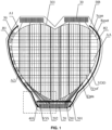
- FIG. 1 is a schematic diagram of a structure of a display substrate provided by an embodiment of the present disclosure
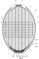
- FIG. 2 is another schematic diagram of a structure of a display substrate provided by an embodiment of the present disclosure
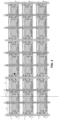
- FIG. 3 is an enlarged schematic diagram of a part surrounded by dotted lines at the bottom of FIG. 1 and FIG. 2 .
- a display substrate according to an embodiment of the present disclosure includes a display region AA and a non-display region BB.
- the display substrate includes: a base substrate, a driving structure layer and a wiring layer which are located in the display region and arranged on the base substrate.
- the driving structure layer is located in the display region AA
- the wiring layer is located in the non-display region BB.
- the driving structure layer includes a first power supply line VDD, a data signal line Data, and a reference signal line Vref which extend in a first direction.
- the wiring layer includes a first power supply wiring 301, a data wiring 201, and a reference wiring 202.
- the special-shaped edge of the display substrates in FIG. 1 and FIG. 2 are different.
- the special-shaped edge in FIG. 1 is heart-shaped, and the special-shaped edge in FIG. 2 is ellipse-shaped.
- the first power supply wiring 301 is electrically connected to the first power supply line VDD
- the data wiring 201 is electrically connected to the data signal line Data
- the reference wiring 202 is electrically connected to the reference signal line Vref.
- the first power supply wiring 301 is located on a first side of the display region
- the data wiring 201 is located on a second side of the display region AA, wherein the first side is different from the second side, and the data wiring 201 and the reference wiring 202 are located on the same side of the display region.
- first side and the second side may be two sides that are oppositely arranged, and the second side is a side away from the first side.
- a and B being oppositely arranged indicates that B is located on a side away from A.
- the first power supply line VDD includes a first terminal A1 and a second terminal A2 which are oppositely arranged.
- a first side refers to the side of the display region close to the first terminal A1 of the first power supply line VDD, and the second side refers to the side close to the second terminal A2 of the first power supply line VDD.
- a resistance of the first power supply line VDD is greater than a resistance of the data signal line Data and greater than a resistance of the reference signal line Vref.
- the base substrate may be a rigid base substrate or a flexible base substrate, wherein the rigid base substrate may be, but is not limited to, one or more of glass and metal foil; the flexible base substrate may be, but is not limited to, one or more of polyethylene terephthalate, ethylene terephthalate, polyether ether ketone, polystyrene, polycarbonate, polyarylate, polyimide, polyvinyl chloride, polyethylene, and textile fibers.
- the first power supply line VDD is configured to continuously provide a high level power signal.
- the display region AA has a special-shaped edge.
- the non-display region BB surrounds the display region AA.
- the edge of the non-display region BB may be a special-shaped edge, and FIG. 1 and FIG. 2 illustrate the edge of the non-display region BB as a special-shaped edge.
- the number of the first power supply wirings 301 is greater than one, and the number of the first power supply lines VDD is greater than one.
- Multiple first power supply wirings 301 correspond to multiple first power supply lines VDD in a one-to-one manner. Each first power supply wiring 301 is connected to a corresponding first power supply line VDD.
- the first power supply wirings 301 and the first power supply lines VDD may be arranged in the same layer or in different layers.
- the number of data wirings 201 is greater than one, and the number of data signal lines Data is greater than one.
- Multiple data wirings 201 correspond to multiple data signal lines Data in a one-to-one manner.
- Each data wiring 201 is connected to a corresponding data signal line Data.
- the data wirings 201 and the data signal lines Data may be arranged in the same layer or in different layers.
- the number of reference wirings 202 is greater than one, and the number of reference signal lines Vref is greater than one.
- Multiple reference wirings 202 correspond to multiple reference signal lines Vref in a one-to-one manner.
- Each reference wiring 202 is connected to a corresponding reference signal line Vref.
- the reference wirings 202 and the reference signal lines Vref may be arranged in the same layer or in different layers.
- the display substrate includes a display region and a non-display region, wherein the display substrate includes a base substrate as well as a driving structure layer and a wiring layer arranged on the base substrate; the driving structure layer is located in the display region, and the wiring layer is located in the non-display region; the driving structure layer includes a first power supply line, a data signal line, and a reference signal line which extend in a first direction; the wiring layer includes a first power supply wiring, a data wiring and a reference wiring; the first power supply wiring is electrically connected to the first power supply line, the data wiring is electrically connected to the data signal line, and the reference wiring is electrically connected to the reference signal line; the first power supply wiring is located on a first side of the display region, and a data wiring is located on the second side of the display region, wherein the second side is different from the first side; the data wiring and the reference wiring are located on the same side of the display region; for the first power supply line, data signal line and reference signal line with the
- a line width of the first power supply line VDD is greater than that of the data signal line Data and greater than the line width of the reference signal line Vref, so that the resistance of the first power supply line VDD can be reduced.
- the line width of the first power supply line VDD in a 55-inch display substrate can be larger than ten microns.
- the display substrate further includes a second power supply line VSS and a second power supply wiring 401 located in the non-display region BB.
- the second power supply line VSS is electrically connected to the second power supply wiring 401, and the second power supply line VSS extends in a second direction.
- the second power supply line VSS and the second power supply wiring 401 are located on the same side of the display region AA, and the second power supply wiring 401 and the data wiring 201 are located on the same side of the display region AA.
- the second direction intersects the first direction, and a plane where the first direction and the second direction are located is a plane where the display substrate is located.
- the first direction is perpendicular to the second direction.
- the second power supply line VSS and the reference wiring 202 are arranged in different layers, and there is an overlapping region between an orthographic projection of the second power supply line VSS on the base substrate and an orthographic projection of the reference wiring 202 on the base substrate; the second power supply line VSS is electrically connected to the reference wiring 202.
- the second power supply line VSS is electrically connected to the reference signal line Vref through the reference wiring 202, which can not only ensure that the signals of the first electrode and the second electrode of a light-emitting element are equal when the pixel driving circuit initializes the first electrode of the light-emitting element, but also ensure the normal display of the display substrate, which improves the display effect of the display substrate and save the signal wiring.
- the second power supply line VSS and the second power supply wiring 401 may be arranged in the same layer or in different layers.
- the second power supply line VSS is configured to continuously provide a low level power signal.
- a voltage value of the power signal of the first power supply line VDD may be greater than a voltage value of the second supply line VSS.
- a display substrate provided by an exemplary embodiment may further include a flexible circuit board (not shown in the figure), a source driving chip 20 and at least one bonding pad 30 which are located in the non-display region BB.
- the bonding pad 30 and the first power supply wiring 301 are located on a same side of the display region AA, and the source driving chip 20 and the data wiring 201 are located on a same side of the display region AA; the source driving chip 20 is located on one side of the second power supply line VSS away from the display region AA.
- the source driving chip is electrically connected to the data wiring 201, and is configured to provide a data signal to the data signal line Data through the data wiring 201.
- the flexible circuit board is electrically connected to the bonding pad 30 and the second power supply wiring 401 respectively, and is configured to supply power to the first power supply wiring 301 through the bonding pad 30, and supply power to the second power supply wiring 401.
- the flexible circuit board may be disposed at any location of the display substrate.
- the flexible circuit board starts supplying power to the first power supply wiring along the side of the first power supply line away from the source driver chip, and starts supplying power to the second power supply wiring along the side of the first power supply line close to the source driving chip, which can greatly reduce the sum of voltage drops of the first power supply line and the second power supply line and improve the display effect of the display substrate.
- the display substrate may further includes: a peripheral circuit board, a flexible signal line, a source driving chip 20 and at least one bonding pad 30 which are located in the non-display region.
- the bonding pad 30 and the first power supply wiring 301 are located on a same side of the display region AA, and the source driving chip 20 and the data wiring 201 are located on a same side of the display region AA; the source driving chip 20 is located on one side of the second power supply line VSS away from the display region AA.
- the source driving chip is electrically connected to the data wiring 201, and is configured to provide a data signal to the data signal line Data through the data wiring 201.
- the peripheral circuit board is electrically connected to the bonding pad, the second power supply wiring, and the source drive chip through the flexible signal line, and is configured to supply power to the first power supply wiring through the bonding pad, and supply power to the second power supply wiring as well as to provide a signal to the source drive chip.
- one terminal of the flexible signal line is bound to the base substrate, and the other terminal is bound to the peripheral circuit board, and the peripheral circuit board supplies power to the first power supply wiring, the second power supply wiring, and the source driving chip arranged on the base substrate through the flexible signal line.
- the peripheral circuit board and the flexible signal line may be disposed at any position of the display substrate.
- the peripheral circuit board and the flexible signal line start supplying power to the first power supply wiring along the side of the first power supply line away from the source driving chip, and start supplying power to the second power supply wiring along the side of the first power supply line close to the source driving chip, which can greatly reduce the sum of voltage drops of the first power supply line and the second power supply line and improve the display effect of the display substrate.
- the size of the bonding pad 30 is considered according to a process accuracy and an expansion amount, and the width of the bonding pad is 100 nm to 200 nm.
- the number of bonding pads is determined according to requirements of display.
- FIG. 1 illustrates two bonding pads as an example
- FIG. 2 illustrates one bonding pad as an example
- the number of source driving chips may be determined according to the size of the display substrate; the greater the size of the display substrate, the greater the number of the source driving chips.
- FIG. 1 and FIG. 2 illustrate one source driving chip as an example.
- FIG. 4 is a schematic diagram of a partial display region of a display substrate provided by an exemplary embodiment
- FIG. 5 is a top view of a first power supply line and a first power supply connection line in an exemplary embodiment.
- the driving structure layer of the display substrate provided by an exemplary embodiment further includes multiple first power supply connection lines VL which are located in the display region AA and extend in a second direction.
- the first power supply connection line VL and the first power supply line VDD are arranged in different layers. There is an overlapping region between an orthographic projection of at least one first power supply connection line VL on the base substrate and an orthographic projection of the first power supply line VDD on the base substrate. Each of the at least one first power supply connection line VL is electrically connected to the first power supply line VDD.
- Each of the at least one first power supply connection line is electrically connected to the first power supply line, which can reduce the display unevenness of the display substrate caused by different voltage drops of different first power supply lines on the display substrate, and improve the display effect of the display substrate.
- the manufacturing material of the first power supply line VDD may be the same as or different from the manufacturing material of the first power supply connection line VL.
- the first power supply connection line VL may be disposed on a side of the first power supply line VDD close to the base substrate.
- the driving structure layer in the display substrate provided by an exemplary embodiment further includes multiple scanning signal lines Scan and multiple reset signal lines Reset which extend in the second direction, as well as multiple driving structures arranged in a matrix, and each first power supply line VDD is arranged between two adjacent driving structures.
- Each driving structure includes a first driving circuit 100A, a second driving circuit 100B, and a third driving circuit 100C arranged in a second direction.
- the driving structure layer may include M rows and N columns of driving structures, wherein M and N may be positive integers greater than 1.
- FIG. 4 illustrates three rows and three columns of driving structures in the driving structure layer as an example.
- the reset signal line Reset and the first power supply connection line VL are configured to define a row of driving structures, and the adjacent first power supply lines are configured to define a column of driving structures.
- FIG. 6 is a schematic diagram of a gate driving circuit provided by an exemplary embodiment.
- a display substrate provided by an exemplary embodiment further includes a gate driving circuit located in a non-display region.
- the gate driving circuit is located on a third side of the display region, wherein the third side is a side different from the first side and the second side.
- the gate driving circuit is electrically connected to the scanning signal line Scan and the reset signal line Reset respectively, and is configured to provide signals to the scanning signal line and the reset signal line.
- the gate driving circuit includes multiple shift registers 50.
- the multiple shift registers are arranged along the edge of the display region.
- Each shift register 50 includes a first shift register GOA1 and a second shift register GOA2.
- the first shift register GOA1 is electrically connected to the scanning signal line Scan, and is configured to provide a signal to the scanning signal line Scan
- the second shift register GAO2 is electrically connected to the reset signal line Reset, and is configured to provide a signal to the reset signal line Reset.
- the multiple first shift registers GOA1 are cascaded
- the multiple second shift registers GOA2 are cascaded.
- the first shift register and the second shift register in each shift register are arranged in a first direction.
- the display substrate further includes a scan wiring SL and a reset wiring RL; the scanning wiring SL is electrically connected to the scanning signal line and the gate driving circuit respectively, and the reset wiring RL is electrically connected to the reset signal line and the gate driving circuit respectively.
- the gate driving circuit includes multiple shift register groups.
- Each shift register group includes at least one shift register; all the shift registers in each shift register group are arranged along the first direction.
- FIG. 6 illustrates a shift register group including four shift registers as an example. The number of shift registers included in each shift register group is related to the boundary of the display region.
- the multiple shift register groups are arranged in a stepped manner, and a distance L between adjacent shift registers in the second direction is greater than a sum of the length of the scanning wiring and the length of the reset wiring length. The smaller the distance between adjacent shift registers in the second direction, the easier it is for the display substrate to realize a narrow bezel.
- the multiple shift register groups are arranged around the edge of the display region, at least partially surrounding the display region.
- the arrangement of shift registers is determined according to the special-shaped boundary.
- the gate driving circuit is located on a third side of the display region.
- the scanning signal line Scan includes a first terminal B1 and a second terminal B2 which are oppositely arranged.
- the third side may be a side close to the first terminal B1 of the scanning signal line Scan or a side close to the second terminal B2 of the scanning signal line Scan.
- the gate driving circuit may be located on the same side of the display substrate as the bonding pad.
- the gate driving circuit, the bonding pad, and the source driving chip are located on different sides of the display substrate.
- the gate driving circuit may be arranged in the non-display region between two bonding pads.
- the display substrate may include two gate driving circuits respectively located on a third side and a fourth side of the display region.
- the two gate driving circuits have the same structure, and multiple shift registers in the two gate driving circuits correspond to each other in a one-to-one manner.
- the corresponding shift registers in the two gate driving circuits are connected to the same scanning signal line and the same reset signal line, and are configured to provide signals to the scanning signal line and the reset signal line in different stages, so that the service life of the display substrate can be prolonged.
- the peripheral circuit board is electrically connected to the gate driving circuit through a flexible signal line, and is configured to provide a signal to the gate driving circuit, wherein the signal includes a clock signal.
- the display substrate further includes a gate signal wiring 501.
- the gate signal wiring 501 is electrically connected to the flexible signal line and the gate driving circuit respectively.
- the display substrate further includes a flexible binding board.
- the flexible binding board can be a chip-on-film thin film.
- the source driving chip may be located on the flexible binding board.
- the flexible binding board can provide signals to a multi-channel control wiring, the first power supply wiring, the second power supply wiring, and the gate signal wiring, wherein the multi-channel control wiring is a control wiring of a multiplexer connected to a source driving chip.
- part of the peripheral wirings may be arranged on the flexible circuit board and part of the peripheral wirings may be arranged on the flexible binding board.
- the flexible circuit board may be connected to the first power supply wiring and the second power supply wiring, and the flexible binding board can provide signals to the multi-channel control wiring and gate signal wiring; or, the flexible circuit board can provide signals to the second power supply wiring and gate signal wiring, and the flexible binding board can provide signals to the first power supply wiring and the multi-channel control wiring.
- the source driving chip may be located on a glass substrate, and the flexible circuit board may be electrically connected to the multi-channel control wiring, the first power supply wiring, the second power supply wiring, and the gate signal wiring.
- data signal lines include: a first data line Data1, a second data line Data2, and a third data line Data3; wherein the first data line Data1 is electrically connected to a first driving circuit 100A, the second data line Data2 is electrically connected to a second driving circuit 100B, and the third data line Data3 is electrically connected to a third driving circuit 100C.
- the reference signal line Vref is electrically connected to the first driving circuit 100A, the second driving circuit 100B and the third driving circuit 100C respectively.
- the first data line Data1 and the second data line Data2 are located between the first driving circuit 100A and the second driving circuit 100B, and the second data line Data2 is located on one side of the first data line Data1 close to the second driving circuit 100B; the third data line Data3 and the reference signal line Vref are located between the second driving circuit 100B and the third driving circuit 100C, and the third data line Data3 is located on the side of the reference signal line Vref close to the third driving circuit 100C; or, the first data line Data1 and the reference signal line Vref are located between the first driving circuit 100A and the second driving circuit 100B, and the first data line Data1 is located on one side of the reference signal line Vref close to the second driving circuit 100B; the second and third data lines Data2 and Data3 are located between the second driving circuit 100B and the third driving circuit 100C, and the third data line Data3 is located on one side of the second data line Data2 close to the third driving circuit 100C.
- FIG. 4 illustrates an example in which the first data line Data1 and
- the data lines and the first power supply lines may be located on both sides of the driving circuit, or the data line and the first power supply line may be located between two driving circuits.
- FIG. 4 illustrates an example in which the data lines and the first power supply lines can be located on both sides of the driving circuit.
- the first driving circuit 100A and the third driving circuit 100C are mirror symmetrical with respect to the center line C of the first data line and the third data line.
- the first driving circuit and the second driving circuit are arranged in mirror symmetrical with respect to the center line of the first data line and the second data line.
- the first driving circuit and the second driving circuit are mirror symmetrical with respect to the center line of the first data line and the reference signal line.
- the display substrate includes a first driving structure, a second driving structure, and a third driving structure which are adjacently arranged in a second direction.
- a third driving circuit in the first driving structure and a first driving circuit in the second driving structure are mirror symmetrical with respect to the first power supply line between the first driving structure and the second driving structure; a third driving circuit in the second driving structure and a first driving circuit in the third driving structure are mirror symmetrical with respect to the first power supply line between the second driving structure and the third driving structure.
- the display substrate further includes a light-emitting structure layer located on one side of the driving structure layer away from the base substrate.
- the light-emitting structure layer includes multiple light-emitting elements.
- Each driving circuit in the driving structure layer includes a pixel driving circuit configured to drive the light-emitting element to emit light, wherein the pixel driving circuit is electrically connected to the light-emitting element.
- the light-emitting element may be an organic light-emitting diode.
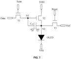
- FIG. 7 is an equivalent circuit diagram of a pixel driving circuit provided by an exemplary embodiment.
- the pixel driving circuit includes a first transistor T1, a second transistor T2, a third transistor T3, and a storage capacitor C ST .
- the first transistor T1 is a switching transistor
- the second transistor T2 is a driving transistor
- the third transistor T3 is a reset transistor.
- the storage capacitor C ST includes a first electrode plate 41 and a second electrode plate 42.
- a control electrode of the first transistor T1 is electrically connected to the scanning signal line Scan, a first electrode of the first transistor T1 is electrically connected to the data signal line Data, and a second electrode of the first transistor T1 is electrically connected to a first node N1.
- a control electrode of the second transistor T2 is electrically connected to the first node N1, a first electrode of the second transistor T2 is electrically connected to the first power supply line VDD, and a second electrode of the second transistor T2 is electrically connected to a second node N2.
- a control electrode of the third transistor T3 is electrically connected to the reset signal line Reset, a first electrode of the third transistor T3 is electrically connected to the reference signal line Vref, a second electrode of the third transistor T3 is electrically connected to the second node N2.
- the first electrode plate 41 of the storage capacitor C ST is electrically connected to the second node N2, and the second electrode plate 42 of the storage capacitor C ST is electrically connected to the first node N1.
- the first electrode of the light-emitting element OLED is electrically connected to the second node N2, and the second electrode of the light-emitting element is electrically connected to the second power supply line VSS.
- the line width of the second power supply line VSS is equal to the line width of the Data signal line Data, which can simplify the manufacturing process.
- the transistors T1 to T3 can all be N-type thin film transistors or P-type thin film transistors, which can unify the process flow, reduce the manufacturing process, and help to improve the yield of the display substrate.
- FIG. 8 is an operation sequence diagram of a pixel driving circuit provided by an exemplary embodiment. As shown in FIG. 7 and FIG. 8 , an operation process of the pixel driving circuit according to an exemplary embodiment includes the following contents.
- the first power supply line VDD continuously provides a high level signal
- the second power supply line VSS and the reference signal line Vref continuously provide low level signals.
- a first stage S1 i.e., a reset stage
- the input signal of the scanning signal line Scan is a high level signal
- the input signal of the reset signal line Reset is a high level signal
- the input signal of the data signal line Data is a low level signal
- the first transistor T1 is turned on, and the low level signal of data signal line Data is written into the first node N1
- the third transistor T3 is turned on, and the low level signal of reference signal line Vref is written into the second node N2. Since the voltage of the second node N2 is the same as the voltage of the second power supply line VSS, the light-emitting element OLED does not emit light.
- a second stage S2 i.e., a compensation stage
- the input signal of the scanning signal line Scan is a high level signal
- the input signal of the reset signal line Reset is a low level signal
- the input signal of the data signal line Data is a low level signal
- the first transistor T1 is turned on
- the low level signal of data signal line Data is written into the first node N1
- the third transistor T3 is turned off.
- the second transistor T2 Since a voltage difference between the signal of the first node N1 and the signal of the second node N2 is greater than the threshold voltage of the second transistor T2, the second transistor T2 is turned on, and the voltage of the second node N2 gradually rises until the voltage of the second node N2 is equal to the difference value between the signal voltage of the first node N1 and the threshold voltage of the second transistor T2. As the voltage of the second node N2 rises gradually, the more the mobility of the second transistor T2 increases, the more the voltage of the second node N2 rises, the smaller the threshold voltage of the second transistor T2 is, and the less the voltage of the second node N2 rises.
- a current difference caused by different mobilities and threshold voltages of the second transistors T2 in different pixel driving circuits can be reduced, which can realize a compensation to the display uniformity of the display substrate, and can improve the display effect of the display substrate.
- a writing stage i.e., a writing stage
- the input signal of scanning signal line Scan is a high level signal
- the input signal of the reset signal line Reset is a low level signal
- the input signal of data signal line Data is a high level signal
- the first transistor T1 is turned on
- the high level signal of data signal line Data is written into the first node N1.
- the voltage value of the signal of the second node N2 will change accordingly due to the action of storage capacitor C ST .
- the duration of this stage is short, the voltage value of the second node N2 will also be changed like the compensation stage, thus achieving an effect of recompensation.
- a fourth stage S4 i.e., a light-emitting stage
- the input signal of the scanning signal line Scan is a low level signal
- the input signal of the reset signal line Reset is a low level signal
- the input signal of the data signal line Data is a low level signal
- the first transistor T1 is turned off
- the second transistor T2 is turned on
- a driving circuit is provided to the light-emitting element OLED, and the light-emitting element OLED emits light.
- the input signal of the data signal line Data changes from low level to high level within one frame, so that the frequency of the input signal of the data signal line Data is higher.
- FIG. 9 is a layout diagram of a driving structure according to an exemplary embodiment.
- a first transistor T1 includes a first active layer 11, a first gate electrode 12, a first source electrode 13, and a first drain electrode 14;
- a second transistor T2 includes a second active layer 21, a second gate electrode 22, a second source electrode 23, and a second drain electrode 24;
- a third transistor T3 includes a third active layer 31, a third gate electrode 32, and a third drain electrode 24.
- a storage capacitor includes a first electrode plate 41 and a second electrode plate 42.
- FIG. 9 illustrates an example in which a first electrode is a source electrode and a second electrode is a drain electrode.
- the driving structure layer further includes a first reference connection line 51 and a second reference connection line 61 which extend in a second direction.
- the first reference connection line 51 and the second reference connection line 61 are arranged in different layers, and the second reference connection line 61 is electrically connected to the reference signal line Vref and the first reference connection line 51 respectively.
- each driving structure includes two first reference connection lines arranged in a first direction and three second reference connection lines arranged in the first direction.
- the first one of the two first reference connection lines is electrically connected to a first one and a second one of the three second reference connection lines respectively; the second one of the two first reference connection lines is electrically connected to the second one and the third one of the three second reference connection lines respectively; the second one of the three second reference connection lines is connected to the reference signal line and they form a continuous integrated structure.
- the scanning signal line Scan is electrically connected to the first gate electrode 12 of the first transistor T1 in each driving structure
- the reset signal line Reset is electrically connected to the third gate electrode 32 of the third transistor T3 in each driving structure
- the data signal line Data is electrically connected to the first source electrode 13 of the first transistor T1 in each driving structure
- the first reference connection line 51 and the second reference connection line 61 are configured to make the third source electrode 33 of the third transistor T3 electrically connect with the reference signal line Vref.
- the first gate electrode 12 of the first transistor T1 is electrically connected to the scanning signal line Scan
- the first source electrode 13 of the first transistor T1 is electrically connected to the data signal line Data
- the first drain electrode 14 of the first transistor T1 is electrically connected to the second gate electrode 22 of the second transistor T2.
- the second gate electrode 22 of the second transistor T2 is electrically connected to the first drain electrode 14 of the first transistor T1
- the second source electrode 23 of the second transistor T2 is electrically connected to the third drain electrode 34 of the third transistor T3 and the first electrode of light-emitting element
- the second drain electrode 24 of the second transistor T2 is electrically connected to the first power supply line VDD
- the third gate electrode 32 of the third transistor T3 is electrically connected to the reset signal line Reset
- the third source electrode 33 of the third transistor T3 is electrically connected to the reference signal line Vref through the first reference connection line 51 and the second reference connection line 61
- the third drain electrode 34 of the third transistor T3 is electrically connected to the second source electrode 23 of the second transistor T2 and the first electrode of the light-emitting element.
- the first electrode plate 41 is electrically connected to the second source electrode 23 of the second transistor T2 and the third drain electrode 34 of the third transistor T3, and the second electrode plate 42 is electrically connected to the first drain electrode 14 of the first transistor T1 and the second gate electrode 22 of the second transistor T2.
- the driving structure layer includes: a first insulating layer, an active layer, a second insulating layer, a first metal layer, a third insulating layer, and a second metal layer which are sequentially arranged along a direction perpendicular to the base substrate.
- the active layer includes active layers of all transistors.
- the active layer of each transistor is arranged on the same layer and formed in the same patterning process.
- the first metal layer includes: a first reference connection line, control electrodes of all transistors, a first electrode plate, a reset signal line, a scanning signal line, and a first power supply connection line.
- the first reference connection line, the control electrodes of all transistors, the first electrode plate, the reset signal line, the scanning signal line, and the first power supply connection line are arranged on the same layer and formed in the same patterning process.
- the second metal layer includes: a second reference connection line, a reference signal line, a data line, a second electrode plate, and first and second electrodes of all transistors.
- the second reference connection line, the reference signal line, the data line, the second electrode plate and the first and second electrodes of all transistors are arranged on the same layer and formed in the same patterning process.
- each transistor is turned on when the gate is applied with a high level (on level), and is turned off when the gate is applied with a low level (off level).
- the first electrode of the transistor may be a source
- the second electrode of the transistor may be a drain.
- the pixel driving circuit includes, but is not limited to, a configuration mode shown in FIG. 7 .
- N-type transistors or a mixture of P-type transistors and N-type transistors may be used as various transistors in the pixel driving circuit, as long as the port polarity of the selected type of transistors is connected according to the port polarity of the corresponding transistors in the embodiment of the disclosure.
- Transistors used in the pixel driving circuit may be thin film transistors, field effect transistors, or other switching devices with the same characteristics.
- thin film transistors are taken as an example.
- the active layer (channel region) of the transistor uses semiconductor materials, such as polysilicon (such as low-temperature polysilicon or high-temperature polysilicon), amorphous silicon, indium gallium tin oxide (IGZO), while the gate, source, and drain electrodes use metal materials, such as metallic aluminum or aluminum alloy.
- the source and drain of the transistor used here may be symmetrical in structure, so there may be no difference between the source and drain in structure.
- one electrode is directly described as the first electrode, and the other electrode is directly described as the second electrode.
- the electrodes of the capacitor may be metal electrodes, or one of the electrodes may use a semiconductor material (e.g., doped polysilicon).
- the first transistor T1 in all driving circuits in each driving structure is located on a side, close to the first power supply connection line VL, of the second electrode plate 42, and the third transistor T3 is located on a side, away from the first power supply connection line VL, of the second electrode plate 42.
- the first transistor in the first driving circuit and the first transistor in the third driving circuit are mirror symmetrical with respect to a center line of two first power supply lines on both sides of the driving structure;
- the second transistor in the first driving circuit and the second transistor in the third driving circuit are mirror symmetrical with respect to a center line of two first power supply lines on both sides of the driving structure;
- the third transistor in the first driving circuit and the third transistor in the third driving circuit are mirror symmetrical with respect to a center line of two first power supply lines on both sides of the driving structure.
- the first transistor in the first driving circuit and the first transistor in the second driving circuit are mirror symmetrical with respect to a center line of the first and the second data lines; the second transistor in the first driving circuit and the second transistor in the second driving circuit are mirror symmetrical with respect to the center line of the first and the second data lines; the third transistor in the first driving circuit and the third transistor in the second driving circuit are mirror symmetrical with respect to the center line of the first and the second data lines.
- the first transistor in the first driving circuit and the first transistor in the second driving circuit are mirror symmetrical with respect to a center line of the first data line and the reference signal line;
- the second transistor in the first driving circuit and the second transistor in the second driving circuit are mirror symmetrical with respect to the center line of the first data line and the reference signal line;
- the third transistor in the first driving circuit and the third transistor in the second driving circuit are mirror symmetrical with respect to the center line of the first data line and the reference signal line.
- the driving structure layer further includes a flat layer located on a side, away from the base substrate, of the second metal layer; a via is arranged on the flat layer, and the via on the flat layer exposes the second source electrode of the second transistor T2.
- the light-emitting structure layer includes: a first electrode, an organic light-emitting layer, and a second electrode.
- the first electrode is located on a side, close to the base substrate, of the organic light-emitting layer
- the second electrode is located on a side, away from the base substrate, of the organic light-emitting layer.
- the first electrode is electrically connected to the second source electrode of the second transistor T2 through the via on the flat layer.
- the third insulating layer is provided with a first via exposing the first power supply connection line VL and a second via exposing the first reference connection line 51.
- the first power supply line VDD is electrically connected to the first power supply connection line VL through the first via; and the second reference connection line 61 is electrically connected to the first reference connection line 51 through the second via.
- the second power supply line VSS is disposed in the same layer as the scanning signal line Scan.
- a connection via exposing the second power supply line is arranged on the third insulating layer, and the reference wiring is electrically connected to the second power supply line through the connection via.
- a shape of the display region may be axial symmetrical or may be non-axial symmetrical.
- the symmetry axis may extend in the first direction or in the second direction.
- the shape of the display region may be circular, elliptical, fan-shaped, heart-shaped, triangular or N-polygonal, wherein N is greater than 4.
- the structure of the display substrate according to an exemplary embodiment will be described as following through the preparation process of the display substrate.
- the "patterning process” includes processes, such as film layer deposition, photoresist coating, mask exposure, development, etching, and photoresist stripping.
- Deposition may be implemented by any one or more of sputtering, evaporation, and chemical vapor deposition
- coating may be implemented by any one or more of spraying and spin coating
- etching may be implemented by any one or more of dry etching and wet etching.
- Thin film refers to a layer of thin film fabricated by a certain material on a base substrate using deposition or coating process.
- the "thin film” may also be called a "layer”. If the "thin film” needs a patterning process throughout the whole manufacturing process, it is referred to as a "thin film” before the patterning process and as a "layer” after the patterning process.
- “A and B are arranged on the same layer” indicates that A and B are formed at the same time in the same patterning process.
- FIG. 10 to FIG. 12 are schematic diagrams of the preparation process of a display substrate according to an exemplary embodiment, illustrating a layout structure of a driving structure of the display substrate, wherein each driving structure includes three driving circuits.
- a pixel driving circuit in each driving circuit includes: a first transistor T1, a second transistor T2, a third transistor T3, and a storage capacitor.
- the first active layer 11 serves as an active layer of the first transistor
- the second active layer 21 serves as an active layer of the second transistor
- the third active layer 31 serves as an active layer of the third transistor.
- orthographic projections of the first active layer 11, the second active layer 21, and the third active layer 31 on the base substrate and that of the first electrode plate 41 on the base substrate are arranged at intervals. That is, there is no overlapping region between the first active layer 11 and the first electrode plate 41, between the second active layer 21 and the first electrode plate 41, or between the third active layer 31 and the first electrode plate 41, which benefits a design of a width-to-length ratio of channels of the first transistor, the second transistor, and the third transistor according to relevant requirements.
- orthographic projections of the first active layer 11, the second active layer 21, and the third active layer 31 on the base substrate and that of the second electrode plate 42 are on the base substrate arranged at intervals. That is, there is no overlapping region between the first active layer 11 and the second electrode plate 42, between the second active layer 21 and the second electrode plate 42, or between the third active layer 31 and the second electrode plate 42, which benefits the design of the width-to-length ratio of channels of the first transistor, the second transistor, and the third transistor according to relevant requirements.
- first metal layer which includes: depositing a second insulating film on the base substrate on which the active layer is formed, patterning the second insulating film through a patterning process to form a second insulating layer in the display region ; depositing a first metal film on the second insulating layer, and patterning the first metal film through a patterning process to form a first metal layer.
- the first metal layer includes: a reset signal line Reset, a scanning signal line Scan, a first power supply connection line VL, a first reference connection line 51, and a first gate electrode 12, a second gate electrode 22, a third gate electrode 32 and a first electrode plate 41 formed in each driving structure, as shown in FIG. 11 .
- the reset signal line Reset, the scanning signal line Scan, the first power supply connection line VL, and the first reference connection line 51 are parallelly arranged and all extend in the first direction.
- the reset signal line Reset and the scanning signal line Scan are respectively located on either side of the first electrode plate 41, the first power supply connection line VL is located on a side, away from the first electrode plate 41, of the scanning signal line Scan, and the first reference connection line 51 is located on a side, away from the first electrode plate 41, of the reset signal line Reset.
- the first gate electrode 12 is an integrated structure connected to the scanning signal line Scan and crosses the first active layer 11.
- the second gate electrode 22 crosses the second active layer 21.
- the third gate electrode 32 is an integrated structure connected to the reset signal line Reset, and crosses the third active layer 31.
- this process further includes a conductive treatment.
- Conduction treatment is that, after the first metal layer is form, plasma treatment is performed on the active layer using the first gate electrode 12, the second gate electrode 22, and the third gate electrode 32 as covers; the active layer in the region covered by the first gate electrode 12, the second gate electrode 22, and the third gate electrode 32 (i.e., the overlapping region between the active layer and the first gate electrode 12, the second gate electrode 22, and the third gate electrode 32) serves as a channel region of the transistor; the active layer in the region which is not covered by the first metal layer is processed into a conductive layer to form a conductive source and drain region.
- Forming a third insulating layer includes: depositing a third insulating film on the base substrate on which the first metal layer is formed, and patterning the third insulating film through a patterning process to form the third insulating layer.
- the third insulating layer is provided with multiple vias.
- the multiple vias include: a first via H1 at the location of the first power supply connection line VL, a second via H2 at the location of the first reference connection line, a third via H3 and a fourth via H4 located on both sides of the first gate electrode 12, a fifth via H5 and a sixth via H6 located on both sides of the second gate electrode 22, a seventh via H7 at the location of the second gate electrode 22, an eighth via H8 located on one side of the third gate electrode 32, a ninth via H9 at the location of the first electrode plate 41, as shown in FIG. 12 .
- the first via H1 exposes a surface of the first power supply connection line VL
- the second via H2 exposes a surface of the first reference connection line 51
- the third via H3 and the fourth via H4 expose surfaces of both terminals of the first active layer 11.
- the fifth and sixth vias H5 and H6 expose surfaces of both terminals of the second active layer 21, the seventh via H7 exposes a surface of the second gate electrode 22, the eighth via H8 exposes a surface of the third active layer 31, and the ninth via H9 exposes a surface of the first electrode plate 41.
- a second metal layer which includes: depositing a second insulating film on the base substrate on which the third insulating layer is formed, patterning the second insulating film through a patterning process to form the second metal layer in the display region on the third insulating layer.
- the second metal layer includes: a first power supply line VDD, three data lines Data, a reference signal line Vref, a second reference connection line 61, as well as a first source electrode 13, a first drain electrode 14, a second source electrode 23, a second drain electrode 24, a third source electrode 33, a third drain electrode 34, and a second electrode plate 42 formed in each driving structure.
- the above content may be understood with reference to FIG. 4 .
- the first power supply line VDD, the data line Data, and the reference signal line Vref are parallelly arranged and extend in the second direction. Two data lines are arranged between the first driving structure and the second driving structure, and another data line and the reference signal line are arranged between the second driving structure and the third driving structure.
- the first power supply line VDD is electrically connected to the first power supply connection line VL through the first via H1.
- the second reference connection line 61 is electrically connected to the first reference connection line 51 through the second via H2.
- the first source electrode 13 is an integrated structure connected to the data signal line Data, so that each data signal line Data is electrically connected to the first source electrode 13 of the driving structure where it is located.
- the first source electrode 13 is electrically connected to one terminal of the first active layer 11 through the third via H3;
- the first drain electrode 14 is electrically connected to the other terminal of the first active layer 11 through the fourth via H4;
- the first drain electrode 14 is also electrically connected to the second gate electrode 22 and the second electrode plate 42 simultaneously through the seventh via H7, so that the first drain electrode 14, the second gate electrode 22, and the second electrode plate 42 have the same potential.
- the second source electrode 23 is electrically connected to one terminal of the second active layer 21 and the first electrode plate 41 simultaneously through the fifth via H5 and the ninth via H9, so that the second source electrode 23, the third drain electrode 34, and the first electrode plate 41 have the same potential.
- the second drain electrode 24 is electrically connected to the other terminal of the second active layer 21 through the sixth via H6.
- the third source electrode 33 is electrically connected to one terminal of the third active layer 31 through the eighth via H8, and is electrically connected to the reference signal line Vref through the second via H2 simultaneously, thus realizing electrical connection between the third source electrode 33 and the reference signal line Vref.
- the second source electrode 23, the third drain electrode 34, and the first electrode plate 41 are connected to each other in an integrated structure.
- the first metal layer and the second metal layer may adopt metal materials, such as any one or more of argentum (Ag), copper (Cu), aluminum (Al) and molybdenum (Mo) or others, or alloy materials of the above metals, such as Aluminum neodymium (AINd) alloy or Molybdenum Niobium (MoNb) alloy, which may have a single-layer structure or a multi-layer composite structure, such as Mo/Cu/Mo.
- metal materials such as any one or more of argentum (Ag), copper (Cu), aluminum (Al) and molybdenum (Mo) or others, or alloy materials of the above metals, such as Aluminum neodymium (AINd) alloy or Molybdenum Niobium (MoNb) alloy, which may have a single-layer structure or a multi-layer composite structure, such as Mo/Cu/Mo.
- the first insulating layer, the second insulating layer, the third insulating layer, and the fourth insulating layer may adopt any one or more of silicon oxide (SiOx), silicon nitride (SiNx) and silicon oxynitride (SiON), and may be a single layer, a multiple layer, or a composite layer.
- the first insulating layer is called a buffer layer, which is configured to improve the water and oxygen resistance of the base substrate
- the second insulating layer is called a gate insulating layer
- the third insulating layer is called an interlayer insulating layer
- the fourth insulating layer is called a passivation layer.
- a thickness of the second insulating layer may be smaller than that of the third insulating layer, and the thickness of the first insulating layer may be smaller than a sum of that of the second insulating layer and that of the third insulating layer, so that the capacity of the storage capacitor can be improved on a premise of ensuring the insulating effect.
- the flat layer may be made of an organic material
- the transparent conductive film may be made of indium tin oxide (ITO) or indium zinc oxide (IZO).
- polyimide, acrylic or polyethylene terephthalate may be used in the pixel define layer.
- any one or more of Magnesium (Mg), Argentum (Ag), Aluminum (Al), copper (Cu) and lithium (Li), or an alloy made of any one or more of the above metals may be used in the second electrode.
- the first insulating layer has a thickness of 3000 to 5000 Angstroms
- the second insulating layer has a thickness of 1000 to 2000 Angstroms
- the third insulating layer has a thickness of 4500 to 7000 Angstroms
- the fourth insulating layer has a thickness of 3000 to 5000 Angstroms.
- the thickness of the first metal layer is 80 to 1200 Angstroms
- the thickness of the second metal layer is 3000 to 5000 Angstroms
- the thickness of the third metal layer is 3000 to 9000 Angstroms.
- the active layer may be a metal oxide layer.
- the metal oxide layer may adopt an oxide containing indium and tin, an oxide containing tungsten and indium, an oxide containing tungsten and indium and zinc, an oxide containing titanium and indium, an oxide containing titanium and indium and tin, an oxide containing indium and zinc, an oxide containing silicon and indium and tin, or an oxide containing indium or gallium and zinc, etc.
- the metal oxide layer may be a single layer, or a double layer, or a multiple layer.
- the structure and preparation process shown in the present disclosure are only an exemplary description.
- the corresponding structure may be changed and the patterning process may be increased or reduced according to actual needs.
- the pixel driving circuit may be 5T1C or 7T1C.
- other electrodes or leads may be provided in the film layer structure.
- An embodiment of the present disclosure also provides a display apparatus, including a display substrate.
- the display apparatus may be: a mobile phone, a tablet computer, a television, a display, a laptop computer, a digital photo frame, a navigator or any product or component with a display function.
- the display substrate according to the present embodiment is the display substrate according to any one of the previous embodiments, and the display substrates are similar in the implementation principle and effect, which will not be described repeatedly here.
Landscapes
- Engineering & Computer Science (AREA)
- Physics & Mathematics (AREA)
- General Physics & Mathematics (AREA)
- Computer Hardware Design (AREA)
- Theoretical Computer Science (AREA)
- Microelectronics & Electronic Packaging (AREA)
- Nonlinear Science (AREA)
- Chemical & Material Sciences (AREA)
- Crystallography & Structural Chemistry (AREA)
- Optics & Photonics (AREA)
- Mathematical Physics (AREA)
- Devices For Indicating Variable Information By Combining Individual Elements (AREA)
- Electroluminescent Light Sources (AREA)
Claims (13)
- Substrat d'affichage, comprenant une région d'affichage (AA) et une région de non-affichage (BB), dans lequel le substrat d'affichage comprend un substrat de base, une couche de structure de commande et une couche de câblage qui sont agencées sur le substrat de base ; la couche de structure de commande est située dans la région d'affichage, et la couche de câblage est située dans la région de non-affichage ;dans lequel la couche de structure de commande comprend : une première ligne d'alimentation électrique (VDD), une ligne de signal de données (Data) et une ligne de signal de référence (Vref) qui s'étendent le long d'une première direction ; la couche de câblage comprend un premier câblage d'alimentation électrique (301), un câblage de données (201) et un câblage de référence (202) ;le premier câblage d'alimentation électrique (301) est connecté électriquement à la première ligne d'alimentation électrique, le câblage de données (201) est connecté électriquement à la ligne de signal de données et le câblage de référence (202) est connecté électriquement à la ligne de signal de référence ;le premier câblage d'alimentation électrique (301) est situé sur un premier côté de la région d'affichage et le câblage de données (201) est situé sur un deuxième côté de la région d'affichage, le deuxième côté étant différent du premier côté ; le câblage de données (201) et le câblage de référence (202) sont situés sur un même côté de la région d'affichage ;pour la première ligne d'alimentation électrique, la ligne de signal de données et la ligne de signal de référence ayant une même longueur, une résistance de la première ligne d'alimentation électrique est supérieure à celle de la ligne de signal de données et supérieure à celle de la ligne de signal de référence, etdans lequel le substrat d'affichage comprend en outre :une deuxième ligne d'alimentation électrique (VSS) et un deuxième câblage d'alimentation électrique (401) qui sont situés dans la région de non-affichage, la deuxième ligne d'alimentation électrique est connectée électriquement au deuxième câblage d'alimentation électrique (401), la deuxième ligne d'alimentation électrique s'étend le long d'une deuxième direction, la deuxième direction est perpendiculaire à la première direction ; la deuxième ligne d'alimentation électrique et le deuxième câblage d'alimentation électrique (401) sont situés sur un même côté de la région d'affichage, et le deuxième câblage d'alimentation électrique (401) et le câblage de données (201) sont situés sur un même côté de la région d'affichage ; etune puce de commande de source (20) et au moins un plot de connexion (30) qui sont situés dans la région de non-affichage, le plot de connexion (30) est connecté électriquement à une carte de circuit imprimé flexible ; le plot de connexion (30) et le premier câblage d'alimentation électrique (301) sont situés sur un même côté de la région d'affichage, et la puce de commande de source (20) et le câblage de données (201) sont situés sur un même côté de la région d'affichage ; la puce de commande de source (20) est située sur un côté, éloignée de la région d'affichage, de la deuxième ligne d'alimentation électrique (VSS) ;dans lequel la deuxième ligne d'alimentation électrique (VSS) et le câblage de référence (202) sont agencés dans des couches différentes, et il existe une région de chevauchement entre une projection orthographique de la deuxième ligne d'alimentation électrique (VSS) sur le substrat de base et celle du câblage de référence (202) sur le substrat de base ; la deuxième ligne d'alimentation électrique (VSS) est connectée électriquement au câblage de référence (202) pour se connecter ainsi à la ligne de signal de référence à travers le câblage de référence ;dans lequel la puce de commande de source (20) est connectée électriquement au câblage de données (201) et est configurée pour fournir un signal de données à la ligne de signal de données à travers le câblage de données (201),dans lequel la carte de circuit imprimé flexible alimente le premier câblage d'alimentation électrique le long du côté de la première ligne d'alimentation électrique éloigné de la puce de commande de source, et alimente le deuxième câblage d'alimentation électrique le long du côté de la première ligne d'alimentation électrique proche de la puce de commande de source (20),dans lequel une forme de la région d'affichage est circulaire, elliptique, en forme d'éventail, en forme de coeur, triangulaire ou N-polygonale, où N est supérieur à 4.
- Substrat d'affichage, selon la revendication 1, dans lequel la couche de structure de commande comprend en outre : une pluralité de premières lignes de connexion d'alimentation situées dans la région d'affichage et s'étendant le long d'une deuxième direction ; la pluralité de premières lignes de connexion d'alimentation et la première ligne d'alimentation sont agencées dans des couches différentes ;
il existe une région de chevauchement entre une projection orthographique d'au moins une première ligne de connexion d'alimentation sur le substrat de base et celle de la première ligne d'alimentation sur le substrat de base ; chacune de la ou des premières lignes de connexion d'alimentation est connectée électriquement à la première ligne d'alimentation. - Substrat d'affichage, selon l'une quelconque des revendications 1 à 2, dans lequel la couche de structure de commande comprend en outre : une pluralité de lignes de signal de balayage (Scan) et de lignes de signal de réinitialisation (Reset) s'étendant le long d'une deuxième direction, et une pluralité de structures de commande disposées dans une matrice, et la première ligne d'alimentation électrique est disposée entre deux structures de commande adjacentes ;
dans lequel chaque structure de commande comprend un premier circuit de commande (100A), un deuxième circuit de commande (100B) et un troisième circuit de commande (100C) qui sont agencés le long de la deuxième direction directe. - Substrat d'affichage, selon la revendication 3, comprenant en outre un circuit de commande de porte situé dans la région de non-affichage ; dans lequel le circuit de commande de porte est situé sur un troisième côté de la région d'affichage, et le troisième côté est différent du premier côté et du deuxième côté ;le circuit de commande de porte est connecté électriquement à une ligne de signal de balayage et à une ligne de signal de réinitialisation, respectivement, et est configuré pour fournir un signal à la ligne de signal de balayage et à la ligne de signal de réinitialisation ;le circuit de commande de porte comprend une pluralité de registres à décalage (50), dont chacun comprend un premier registre à décalage et un deuxième registre à décalage ; dans lequel le premier registre à décalage est connecté électriquement à la ligne de signal de balayage, et est configuré pour fournir un signal à la ligne de signal de balayage ; le deuxième registre à décalage est connecté électriquement à la ligne de signal de réinitialisation, et est configuré pour fournir un signal à la ligne de signal de réinitialisation ; une pluralité de premiers registres à décalage sont mis en cascade et une pluralité de deuxièmes registres à décalage sont mis en cascade ;comprenant en outre un câblage de balayage (SL) et un câblage de réinitialisation (RL) ; dans lequel le câblage de balayage est connecté électriquement à la ligne de signal de balayage (Scan) et au circuit de commande de porte respectivement, et le câblage de réinitialisation est connecté électriquement à la ligne de signal de réinitialisation et au circuit de commande de porte respectivement ;le circuit de commande de porte comprend une pluralité de groupes de registres à décalage, chaque groupe de registres à décalage comprend au moins un registre à décalage ; tous les registres à décalage dans chaque groupe de registres à décalage sont agencés le long de la première direction ;la pluralité de groupes de registres à décalage sont disposés de manière étagée, et une distance entre des registres à décalage adjacents le long de la deuxième direction est supérieure à une somme d'une longueur du câblage de balayage et d'une longueur du câblage de réinitialisation.
- Substrat d'affichage, selon la revendication 3, dans lequel dans chaque structure de commande, la ligne de signal de données comprend une première ligne de données (Data1), une deuxième ligne de données (Data2) et une troisième ligne de données (Data3) ; la première ligne de données est électriquement connectée au premier circuit de commande (100A), la deuxième ligne de données est électriquement connectée au deuxième circuit de commande (100B) et la troisième ligne de données est électriquement connectée au troisième circuit de commande (100C) ; la ligne de signal de référence est connectée électriquement au premier circuit de commande (100A), au deuxième circuit de commande (100B) et au troisième circuit de commande (100C) respectivement ;la première ligne de données et la deuxième ligne de données sont situées entre le premier circuit de commande (100A) et le deuxième circuit de commande (100B), et la deuxième ligne de données est située sur un côté, à proximité du deuxième circuit de commande (100B), de la première ligne de données ; la troisième ligne de données et la ligne de signal de référence sont situées entre le deuxième circuit de commande (100B) et le troisième circuit de commande, et la troisième ligne de données est située d'un côté, à proximité du troisième circuit de commande (100C), de la ligne de signal de référence ;dans lequel la première ligne de données et la ligne de signal de référence sont situées entre le premier circuit de commande (100A) et le deuxième circuit de commande (100B), et la première ligne de données est située d'un côté, à proximité du deuxième circuit de commande (100B), de la ligne de signal de référence ; la deuxième ligne de données et la troisième ligne de données sont situées entre le deuxième circuit de commande (100B) et le troisième circuit de commande, et la troisième ligne de données est située sur un côté, à proximité du troisième circuit de commande (100C), de la deuxième ligne de données ;dans chaque structure de commande, le premier circuit de commande (100A) et le troisième circuit de commande (100C) sont symétriques en miroir par rapport à une ligne centrale de la première ligne de données et de la troisième ligne de données
- Substrat d'affichage, selon la revendication 3, comprenant une première structure de commande, une deuxième structure de commande et une troisième structure de commande qui sont agencées de manière adjacente le long de la deuxième direction ;le troisième circuit de commande (100C) dans la première structure de commande et le premier circuit de commande (100A) dans la deuxième structure de commande sont symétriques en miroir par rapport à une première ligne d'alimentation électrique située entre la première structure de commande et la deuxième structure de commande ;le troisième circuit de commande (100C) dans la deuxième structure de commande et le premier circuit de commande (100A) dans la troisième structure de commande sont symétriques en miroir par rapport à une première ligne d'alimentation électrique située entre la deuxième structure de commande et la troisième structure de commande.
- Substrat d'affichage, selon la revendication 3, dans lequel la couche de structure de commande comprend en outre une première ligne de connexion de référence (51) et une deuxième ligne de connexion de référence (61) qui s'étendent le long de la deuxième direction ;
la première ligne de connexion de référence (51) et la deuxième ligne de connexion de référence (61) sont agencées dans des couches différentes ; et la deuxième ligne de connexion de référence (61) est connectée électriquement à la ligne de signal de référence et à la première ligne de connexion de référence (51) respectivement. - Substrat d'affichage, selon l'une quelconque des revendications 1 à 7, comprenant en outre une couche de structure électroluminescente située sur un côté, éloignée du substrat de base, de la couche de structure de commande, la couche de structure électroluminescente comprenant une pluralité d'éléments électroluminescents ;chaque circuit de commande dans la couche de structure de commande comprend un circuit de commande de pixel configuré pour commander un élément électroluminescent pour émettre de la lumière ;le circuit de commande de pixel comprend : un premier transistor (T1), un deuxième transistor (T2), un troisième transistor (T3) et un condensateur de stockage (CST) ; le deuxième transistor est un transistor de commande, et le condensateur de stockage comprend une première plaque d'électrode (41) et une deuxième plaque d'électrode (42) ;une électrode de control du premier transistor est connectée électriquement à une ligne de signal de balayage, une première électrode du premier transistor est connectée électriquement à une ligne de signal de données, et une deuxième électrode du premier transistor est connectée électriquement à un premier noeud ; une électrode de control du deuxième transistor est connectée électriquement à un premier noeud, une première électrode du deuxième transistor est connectée électriquement à une première ligne d'alimentation électrique, et une deuxième électrode du deuxième transistor est connectée électriquement à un deuxième noeud ; une électrode de control du troisième transistor est connectée électriquement à une ligne de signal de réinitialisation, une première électrode du troisième transistor est connectée électriquement à une ligne de signal de référence, une deuxième électrode du troisième transistor est connectée électriquement au deuxième noeud, la première plaque d'électrode du condensateur de stockage est connectée électriquement au deuxième noeud ; et la deuxième plaque d'électrode du condensateur de stockage est connectée électriquement au premier noeud ;une première électrode de l'élément électroluminescent est connectée électriquement au deuxième noeud, et une deuxième électrode de l'élément électroluminescent est connectée électriquement à une deuxième ligne d'alimentation électrique.
- Substrat d'affichage, selon la revendication 8, dans lequel la couche de structure de commande comprend une première couche isolante, une couche active, une deuxième couche isolante, une première couche métallique, une troisième couche isolante et une deuxième couche métallique, qui sont agencées séquentiellement le long d'une direction perpendiculaire au substrat de base ;
la couche active comprend des couches actives de tous les transistors ; la première couche métallique comprend : une première ligne de connexion de référence (51), des électrodes de commande de tous les transistors, une première plaque d'électrode, une ligne de signal de réinitialisation, une ligne de signal de balayage et une première ligne de connexion d'alimentation électrique ; la deuxième couche métallique comprend : une deuxième ligne de connexion de référence (61), une ligne de signal de référence, une ligne de données, une deuxième plaque d'électrode et des première et deuxième électrodes de tous les transistors. - Substrat d'affichage, selon la revendication 9, dans lequel la troisième couche isolante est pourvue d'un premier via exposant la première ligne de connexion d'alimentation électrique, et d'un deuxième via exposant la première ligne de connexion de référence (51) ;
la première ligne d'alimentation électrique est connectée électriquement à la première ligne de connexion d'alimentation électrique par l'intermédiaire du premier via, et la deuxième ligne de connexion de référence (61) est connectée électriquement à la première ligne de connexion de référence (51) par l'intermédiaire du deuxième via. - Substrat d'affichage, selon la revendication 9, dans lequel la deuxième ligne d'alimentation électrique est disposée dans une même couche que la ligne de signal de balayage ;un via de connexion exposant la deuxième ligne d'alimentation électrique est disposé sur la troisième couche isolante ;le câblage de référence (202) est connecté électriquement à la deuxième ligne d'alimentation électrique à travers le via de connexion.
- Substrat d'affichage, selon la revendication 9, dans lequel la couche de structure électroluminescente comprend : une première électrode, une couche électroluminescente organique et une deuxième électrode ; la première électrode est située sur un côté, proche du substrat de base, de la couche électroluminescente organique, et la deuxième électrode est située sur un côté, éloignée du substrat de base, de la couche électroluminescente organique ;
il existe une région de chevauchement entre une projection orthographique de la deuxième électrode sur le substrat de base et celle de la deuxième ligne d'alimentation électrique sur le substrat de base, et la deuxième électrode est connectée électriquement à la deuxième ligne d'alimentation électrique. - Appareil d'affichage, comprenant : le substrat d'affichage selon l'une quelconque des revendications 1 à 12.
Applications Claiming Priority (1)
| Application Number | Priority Date | Filing Date | Title |
|---|---|---|---|
| PCT/CN2020/093492 WO2021237725A1 (fr) | 2020-05-29 | 2020-05-29 | Substrat d'affichage et dispositif d'affichage |
Publications (3)
| Publication Number | Publication Date |
|---|---|
| EP3992705A1 EP3992705A1 (fr) | 2022-05-04 |
| EP3992705A4 EP3992705A4 (fr) | 2022-09-07 |
| EP3992705B1 true EP3992705B1 (fr) | 2024-11-06 |
Family
ID=78745339
Family Applications (1)
| Application Number | Title | Priority Date | Filing Date |
|---|---|---|---|
| EP20904248.0A Active EP3992705B1 (fr) | 2020-05-29 | 2020-05-29 | Substrat d'affichage et dispositif d'affichage |
Country Status (4)
| Country | Link |
|---|---|
| US (1) | US11758780B2 (fr) |
| EP (1) | EP3992705B1 (fr) |
| CN (1) | CN114072724B (fr) |
| WO (1) | WO2021237725A1 (fr) |
Families Citing this family (20)
| Publication number | Priority date | Publication date | Assignee | Title |
|---|---|---|---|---|
| CN114822349A (zh) * | 2022-04-06 | 2022-07-29 | Tcl华星光电技术有限公司 | 一种显示面板 |
| CN117501850A (zh) * | 2022-05-31 | 2024-02-02 | 京东方科技集团股份有限公司 | 显示基板及其制备方法、显示装置 |
| CN114911376B (zh) * | 2022-05-31 | 2025-10-31 | 武汉天马微电子有限公司 | 一种触控面板和触控显示装置 |
| CN119213483B (zh) * | 2022-06-02 | 2026-02-17 | 京东方科技集团股份有限公司 | 显示基板和显示装置 |
| CN114784082B (zh) * | 2022-06-15 | 2022-09-30 | 京东方科技集团股份有限公司 | 显示基板和显示装置 |
| CN117796158A (zh) | 2022-07-27 | 2024-03-29 | 京东方科技集团股份有限公司 | 印刷电路板、包括该印刷电路板的显示设备和图像显示系统 |
| CN115274806B (zh) * | 2022-08-01 | 2025-09-16 | 武汉天马微电子有限公司 | 显示基板、显示面板及显示装置 |
| US12474799B2 (en) | 2022-09-29 | 2025-11-18 | Chengdu Boe Optoelectronics Technology Co., Ltd. | Touch display panel and display apparatus |
| CN115835723A (zh) * | 2022-12-08 | 2023-03-21 | 京东方科技集团股份有限公司 | 显示基板、显示装置 |
| CN116207107A (zh) * | 2023-02-16 | 2023-06-02 | 昆山国显光电有限公司 | 阵列基板、显示面板及显示装置 |
| US20240292660A1 (en) * | 2023-02-23 | 2024-08-29 | Google Llc | Enlarging Active Areas of Displays Using Variable Pixel and/or Transistor Densities |
| US12396341B2 (en) * | 2023-02-23 | 2025-08-19 | Google Llc | Enlarging active areas of displays in electronic devices |
| CN116234385A (zh) * | 2023-03-15 | 2023-06-06 | 合肥京东方卓印科技有限公司 | 显示基板及显示装置 |
| CN116819838A (zh) * | 2023-05-24 | 2023-09-29 | 厦门天马微电子有限公司 | 显示面板、显示装置及其制作方法 |
| CN116721621B (zh) * | 2023-06-20 | 2025-12-05 | 芯颖科技有限公司 | 屏幕显示控制方法、装置、电子设备及可读存储介质 |
| CN121569270A (zh) | 2023-07-17 | 2026-02-24 | 谷歌有限责任公司 | 触摸传感器与经扩大活动区域显示器的集成 |
| CN120130149A (zh) * | 2023-10-10 | 2025-06-10 | 京东方科技集团股份有限公司 | 显示基板及显示装置 |
| CN118486250B (zh) * | 2024-04-30 | 2025-12-02 | 武汉天马微电子有限公司 | 一种显示面板和显示装置 |
| CN121306023A (zh) * | 2024-07-05 | 2026-01-09 | 华为技术有限公司 | 屏幕组件及电子设备 |
| CN119600895B (zh) * | 2024-12-10 | 2026-02-17 | 天马新型显示技术研究院(厦门)有限公司 | 一种显示面板及显示装置 |
Family Cites Families (12)
| Publication number | Priority date | Publication date | Assignee | Title |
|---|---|---|---|---|
| JP2933816B2 (ja) * | 1993-07-15 | 1999-08-16 | シャープ株式会社 | 液晶表示素子及びその製造方法 |
| JP2000147538A (ja) * | 1998-11-12 | 2000-05-26 | Toshiba Corp | 平面表示装置 |
| TW200729129A (en) * | 2006-01-17 | 2007-08-01 | Chi Mei El Corp | Flat panel display and its testing method |
| CN101101390A (zh) * | 2007-06-26 | 2008-01-09 | 河北冀雅电子有限公司 | 一种液晶显示器件布线补偿方法 |
| KR101535929B1 (ko) | 2008-12-02 | 2015-07-10 | 삼성디스플레이 주식회사 | 표시기판, 이를 갖는 표시패널 및 이를 갖는 표시장치 |
| KR102295874B1 (ko) * | 2014-07-24 | 2021-08-31 | 엘지디스플레이 주식회사 | 디스플레이 장치 |
| KR102370353B1 (ko) * | 2015-02-13 | 2022-03-07 | 삼성디스플레이 주식회사 | 디스플레이 장치 |
| KR102342556B1 (ko) * | 2015-07-31 | 2021-12-23 | 엘지전자 주식회사 | 반도체 발광 소자를 이용한 디스플레이 장치 |
| KR102379775B1 (ko) * | 2015-08-31 | 2022-03-29 | 엘지디스플레이 주식회사 | 표시장치 |
| TWI602002B (zh) * | 2016-11-30 | 2017-10-11 | 友達光電股份有限公司 | 顯示面板 |
| CN107705756B (zh) * | 2017-11-22 | 2020-01-07 | 武汉天马微电子有限公司 | 一种显示面板及显示装置 |
| CN108831306A (zh) * | 2018-06-22 | 2018-11-16 | 武汉华星光电半导体显示技术有限公司 | 显示面板及电子设备 |
-
2020
- 2020-05-29 EP EP20904248.0A patent/EP3992705B1/fr active Active
- 2020-05-29 WO PCT/CN2020/093492 patent/WO2021237725A1/fr not_active Ceased
- 2020-05-29 CN CN202080000853.9A patent/CN114072724B/zh active Active
- 2020-05-29 US US17/273,290 patent/US11758780B2/en active Active
Also Published As
| Publication number | Publication date |
|---|---|
| CN114072724A (zh) | 2022-02-18 |
| WO2021237725A1 (fr) | 2021-12-02 |
| EP3992705A1 (fr) | 2022-05-04 |
| CN114072724B (zh) | 2023-06-27 |
| WO2021237725A9 (fr) | 2022-06-30 |
| US20220254857A1 (en) | 2022-08-11 |
| EP3992705A4 (fr) | 2022-09-07 |
| US11758780B2 (en) | 2023-09-12 |
Similar Documents
| Publication | Publication Date | Title |
|---|---|---|
| US11758780B2 (en) | Display substrate and display apparatus | |
| CN112071882B (zh) | 显示基板及其制备方法、显示装置 | |
| US12469456B2 (en) | Display substrate with optimized fan-out structure, preparation method thereof, and display apparatus | |
| US20240397762A1 (en) | Display Substrate and Display Apparatus | |
| US11721291B2 (en) | Display substrate and display apparatus | |
| US12315456B2 (en) | Display apparatus with compensation and driving method therefor | |
| US12426365B2 (en) | Display substrate and manufacturing method therefor, and display device | |
| US12356810B2 (en) | Display substrate with stepped wire configuration, dummy rectangle units and display apparatus, and manufacturing method thereof | |
| US12230215B2 (en) | Display substrate, manufacturing method therefor, and display apparatus | |
| US12408432B2 (en) | Display substrate and manufacturing method therefor, and display device | |
| US20250174188A1 (en) | Display substrate, preparation method thereof, and display apparatus | |
| US12315442B2 (en) | Display device and driving method therefor | |
| US12579935B2 (en) | Pixel circuit having a node control sub-circuit, driving method therefor, display substrate, and display apparatus | |
| US20250160156A1 (en) | Display Substrate Having Bezel Region at Periphery of First Display Region and Second Display Region and Preparation Method Thereof, and Display Apparatus Having The Same | |
| US12563922B2 (en) | Display substrate, preparing method therefor, and display apparatus | |
| US20240306461A1 (en) | Display Substrate and Preparation Method therefor, and Display Apparatus | |
| US12578813B2 (en) | Touch display substrate, manufacturing method therefor, and touch display device | |
| US20230180521A1 (en) | Display Substrate, Preparation Method thereof, and Display Apparatus | |
| US20250098450A1 (en) | Display Substrate and Display Apparatus | |
| US12575281B2 (en) | Display substrate and preparation method therefor, and display apparatus | |
| US20250126987A1 (en) | Display Substrate and Display Apparatus | |
| CN116456772A (zh) | 显示基板及其制备方法、显示装置 | |
| US12628514B2 (en) | Display substrate, manufacturing method therefor, and display apparatus | |
| US20240324373A1 (en) | Display Substrate and Display Apparatus | |
| WO2026092051A1 (fr) | Substrat d'affichage et dispositif d'affichage |
Legal Events
| Date | Code | Title | Description |
|---|---|---|---|
| STAA | Information on the status of an ep patent application or granted ep patent |
Free format text: STATUS: UNKNOWN |
|
| STAA | Information on the status of an ep patent application or granted ep patent |
Free format text: STATUS: THE INTERNATIONAL PUBLICATION HAS BEEN MADE |
|
| PUAI | Public reference made under article 153(3) epc to a published international application that has entered the european phase |
Free format text: ORIGINAL CODE: 0009012 |
|
| STAA | Information on the status of an ep patent application or granted ep patent |
Free format text: STATUS: REQUEST FOR EXAMINATION WAS MADE |
|
| 17P | Request for examination filed |
Effective date: 20210629 |
|
| AK | Designated contracting states |
Kind code of ref document: A1 Designated state(s): AL AT BE BG CH CY CZ DE DK EE ES FI FR GB GR HR HU IE IS IT LI LT LU LV MC MK MT NL NO PL PT RO RS SE SI SK SM TR |
|
| A4 | Supplementary search report drawn up and despatched |
Effective date: 20220804 |
|
| RIC1 | Information provided on ipc code assigned before grant |
Ipc: H01L 27/32 20060101ALI20220801BHEP Ipc: G09F 9/30 20060101ALI20220801BHEP Ipc: G02F 1/1345 20060101AFI20220801BHEP |
|
| STAA | Information on the status of an ep patent application or granted ep patent |
Free format text: STATUS: EXAMINATION IS IN PROGRESS |
|
| 17Q | First examination report despatched |
Effective date: 20230428 |
|
| DAV | Request for validation of the european patent (deleted) | ||
| DAX | Request for extension of the european patent (deleted) | ||
| GRAP | Despatch of communication of intention to grant a patent |
Free format text: ORIGINAL CODE: EPIDOSNIGR1 |
|
| STAA | Information on the status of an ep patent application or granted ep patent |
Free format text: STATUS: GRANT OF PATENT IS INTENDED |
|
| RIC1 | Information provided on ipc code assigned before grant |
Ipc: G09F 9/30 20060101ALI20240621BHEP Ipc: G02F 1/1345 20060101AFI20240621BHEP |
|
| INTG | Intention to grant announced |
Effective date: 20240709 |
|
| GRAS | Grant fee paid |
Free format text: ORIGINAL CODE: EPIDOSNIGR3 |
|
| GRAA | (expected) grant |
Free format text: ORIGINAL CODE: 0009210 |
|
| STAA | Information on the status of an ep patent application or granted ep patent |
Free format text: STATUS: THE PATENT HAS BEEN GRANTED |
|
| AK | Designated contracting states |
Kind code of ref document: B1 Designated state(s): AL AT BE BG CH CY CZ DE DK EE ES FI FR GB GR HR HU IE IS IT LI LT LU LV MC MK MT NL NO PL PT RO RS SE SI SK SM TR |
|
| REG | Reference to a national code |
Ref country code: GB Ref legal event code: FG4D |
|
| REG | Reference to a national code |
Ref country code: CH Ref legal event code: EP |
|
| REG | Reference to a national code |
Ref country code: DE Ref legal event code: R096 Ref document number: 602020041087 Country of ref document: DE |
|
| REG | Reference to a national code |
Ref country code: IE Ref legal event code: FG4D |
|
| REG | Reference to a national code |
Ref country code: LT Ref legal event code: MG9D |
|
| REG | Reference to a national code |
Ref country code: NL Ref legal event code: MP Effective date: 20241106 |
|
| PG25 | Lapsed in a contracting state [announced via postgrant information from national office to epo] |
Ref country code: IS Free format text: LAPSE BECAUSE OF FAILURE TO SUBMIT A TRANSLATION OF THE DESCRIPTION OR TO PAY THE FEE WITHIN THE PRESCRIBED TIME-LIMIT Effective date: 20250306 Ref country code: PT Free format text: LAPSE BECAUSE OF FAILURE TO SUBMIT A TRANSLATION OF THE DESCRIPTION OR TO PAY THE FEE WITHIN THE PRESCRIBED TIME-LIMIT Effective date: 20250306 Ref country code: HR Free format text: LAPSE BECAUSE OF FAILURE TO SUBMIT A TRANSLATION OF THE DESCRIPTION OR TO PAY THE FEE WITHIN THE PRESCRIBED TIME-LIMIT Effective date: 20241106 |
|
| PG25 | Lapsed in a contracting state [announced via postgrant information from national office to epo] |
Ref country code: FI Free format text: LAPSE BECAUSE OF FAILURE TO SUBMIT A TRANSLATION OF THE DESCRIPTION OR TO PAY THE FEE WITHIN THE PRESCRIBED TIME-LIMIT Effective date: 20241106 Ref country code: NL Free format text: LAPSE BECAUSE OF FAILURE TO SUBMIT A TRANSLATION OF THE DESCRIPTION OR TO PAY THE FEE WITHIN THE PRESCRIBED TIME-LIMIT Effective date: 20241106 |
|
| REG | Reference to a national code |
Ref country code: AT Ref legal event code: MK05 Ref document number: 1740014 Country of ref document: AT Kind code of ref document: T Effective date: 20241106 |
|
| PG25 | Lapsed in a contracting state [announced via postgrant information from national office to epo] |
Ref country code: BG Free format text: LAPSE BECAUSE OF FAILURE TO SUBMIT A TRANSLATION OF THE DESCRIPTION OR TO PAY THE FEE WITHIN THE PRESCRIBED TIME-LIMIT Effective date: 20241106 |
|
| PG25 | Lapsed in a contracting state [announced via postgrant information from national office to epo] |
Ref country code: ES Free format text: LAPSE BECAUSE OF FAILURE TO SUBMIT A TRANSLATION OF THE DESCRIPTION OR TO PAY THE FEE WITHIN THE PRESCRIBED TIME-LIMIT Effective date: 20241106 |
|
| PG25 | Lapsed in a contracting state [announced via postgrant information from national office to epo] |
Ref country code: NO Free format text: LAPSE BECAUSE OF FAILURE TO SUBMIT A TRANSLATION OF THE DESCRIPTION OR TO PAY THE FEE WITHIN THE PRESCRIBED TIME-LIMIT Effective date: 20250206 |
|
| PG25 | Lapsed in a contracting state [announced via postgrant information from national office to epo] |
Ref country code: LV Free format text: LAPSE BECAUSE OF FAILURE TO SUBMIT A TRANSLATION OF THE DESCRIPTION OR TO PAY THE FEE WITHIN THE PRESCRIBED TIME-LIMIT Effective date: 20241106 Ref country code: GR Free format text: LAPSE BECAUSE OF FAILURE TO SUBMIT A TRANSLATION OF THE DESCRIPTION OR TO PAY THE FEE WITHIN THE PRESCRIBED TIME-LIMIT Effective date: 20250207 Ref country code: AT Free format text: LAPSE BECAUSE OF FAILURE TO SUBMIT A TRANSLATION OF THE DESCRIPTION OR TO PAY THE FEE WITHIN THE PRESCRIBED TIME-LIMIT Effective date: 20241106 |
|
| PG25 | Lapsed in a contracting state [announced via postgrant information from national office to epo] |
Ref country code: PL Free format text: LAPSE BECAUSE OF FAILURE TO SUBMIT A TRANSLATION OF THE DESCRIPTION OR TO PAY THE FEE WITHIN THE PRESCRIBED TIME-LIMIT Effective date: 20241106 |
|
| PG25 | Lapsed in a contracting state [announced via postgrant information from national office to epo] |
Ref country code: RS Free format text: LAPSE BECAUSE OF FAILURE TO SUBMIT A TRANSLATION OF THE DESCRIPTION OR TO PAY THE FEE WITHIN THE PRESCRIBED TIME-LIMIT Effective date: 20250206 |
|
| PG25 | Lapsed in a contracting state [announced via postgrant information from national office to epo] |
Ref country code: SM Free format text: LAPSE BECAUSE OF FAILURE TO SUBMIT A TRANSLATION OF THE DESCRIPTION OR TO PAY THE FEE WITHIN THE PRESCRIBED TIME-LIMIT Effective date: 20241106 |
|
| PGFP | Annual fee paid to national office [announced via postgrant information from national office to epo] |
Ref country code: DE Payment date: 20250519 Year of fee payment: 6 |
|
| PG25 | Lapsed in a contracting state [announced via postgrant information from national office to epo] |
Ref country code: DK Free format text: LAPSE BECAUSE OF FAILURE TO SUBMIT A TRANSLATION OF THE DESCRIPTION OR TO PAY THE FEE WITHIN THE PRESCRIBED TIME-LIMIT Effective date: 20241106 |
|
| PG25 | Lapsed in a contracting state [announced via postgrant information from national office to epo] |
Ref country code: EE Free format text: LAPSE BECAUSE OF FAILURE TO SUBMIT A TRANSLATION OF THE DESCRIPTION OR TO PAY THE FEE WITHIN THE PRESCRIBED TIME-LIMIT Effective date: 20241106 |
|
| PG25 | Lapsed in a contracting state [announced via postgrant information from national office to epo] |
Ref country code: RO Free format text: LAPSE BECAUSE OF FAILURE TO SUBMIT A TRANSLATION OF THE DESCRIPTION OR TO PAY THE FEE WITHIN THE PRESCRIBED TIME-LIMIT Effective date: 20241106 |
|
| PG25 | Lapsed in a contracting state [announced via postgrant information from national office to epo] |
Ref country code: SK Free format text: LAPSE BECAUSE OF FAILURE TO SUBMIT A TRANSLATION OF THE DESCRIPTION OR TO PAY THE FEE WITHIN THE PRESCRIBED TIME-LIMIT Effective date: 20241106 |
|
| PG25 | Lapsed in a contracting state [announced via postgrant information from national office to epo] |
Ref country code: CZ Free format text: LAPSE BECAUSE OF FAILURE TO SUBMIT A TRANSLATION OF THE DESCRIPTION OR TO PAY THE FEE WITHIN THE PRESCRIBED TIME-LIMIT Effective date: 20241106 |
|
| PG25 | Lapsed in a contracting state [announced via postgrant information from national office to epo] |
Ref country code: IT Free format text: LAPSE BECAUSE OF FAILURE TO SUBMIT A TRANSLATION OF THE DESCRIPTION OR TO PAY THE FEE WITHIN THE PRESCRIBED TIME-LIMIT Effective date: 20241106 |
|
| REG | Reference to a national code |
Ref country code: DE Ref legal event code: R097 Ref document number: 602020041087 Country of ref document: DE |
|
| PG25 | Lapsed in a contracting state [announced via postgrant information from national office to epo] |
Ref country code: SE Free format text: LAPSE BECAUSE OF FAILURE TO SUBMIT A TRANSLATION OF THE DESCRIPTION OR TO PAY THE FEE WITHIN THE PRESCRIBED TIME-LIMIT Effective date: 20241106 |
|
| PLBE | No opposition filed within time limit |
Free format text: ORIGINAL CODE: 0009261 |
|
| STAA | Information on the status of an ep patent application or granted ep patent |
Free format text: STATUS: NO OPPOSITION FILED WITHIN TIME LIMIT |
|
| 26N | No opposition filed |
Effective date: 20250807 |
|
| REG | Reference to a national code |
Ref country code: CH Ref legal event code: H13 Free format text: ST27 STATUS EVENT CODE: U-0-0-H10-H13 (AS PROVIDED BY THE NATIONAL OFFICE) Effective date: 20251223 |
|
| PG25 | Lapsed in a contracting state [announced via postgrant information from national office to epo] |
Ref country code: LU Free format text: LAPSE BECAUSE OF NON-PAYMENT OF DUE FEES Effective date: 20250529 |
|
| PG25 | Lapsed in a contracting state [announced via postgrant information from national office to epo] |
Ref country code: CH Free format text: LAPSE BECAUSE OF NON-PAYMENT OF DUE FEES Effective date: 20250531 |
|
| REG | Reference to a national code |
Ref country code: BE Ref legal event code: MM Effective date: 20250531 |
|
| PG25 | Lapsed in a contracting state [announced via postgrant information from national office to epo] |
Ref country code: MC Free format text: LAPSE BECAUSE OF FAILURE TO SUBMIT A TRANSLATION OF THE DESCRIPTION OR TO PAY THE FEE WITHIN THE PRESCRIBED TIME-LIMIT Effective date: 20241106 |
|
| PGFP | Annual fee paid to national office [announced via postgrant information from national office to epo] |
Ref country code: GB Payment date: 20260323 Year of fee payment: 7 |
|
| PG25 | Lapsed in a contracting state [announced via postgrant information from national office to epo] |
Ref country code: IE Free format text: LAPSE BECAUSE OF NON-PAYMENT OF DUE FEES Effective date: 20250529 |
|
| PG25 | Lapsed in a contracting state [announced via postgrant information from national office to epo] |
Ref country code: BE Free format text: LAPSE BECAUSE OF NON-PAYMENT OF DUE FEES Effective date: 20250531 |
|
| PG25 | Lapsed in a contracting state [announced via postgrant information from national office to epo] |
Ref country code: FR Free format text: LAPSE BECAUSE OF NON-PAYMENT OF DUE FEES Effective date: 20250531 |