EP3992706B1 - Affichages électro-optiques stratifiés et procédés de fabrication - Google Patents
Affichages électro-optiques stratifiés et procédés de fabrication Download PDFInfo
- Publication number
- EP3992706B1 EP3992706B1 EP21206101.4A EP21206101A EP3992706B1 EP 3992706 B1 EP3992706 B1 EP 3992706B1 EP 21206101 A EP21206101 A EP 21206101A EP 3992706 B1 EP3992706 B1 EP 3992706B1
- Authority
- EP
- European Patent Office
- Prior art keywords
- electro
- layer
- optic
- display
- backplane
- Prior art date
- Legal status (The legal status is an assumption and is not a legal conclusion. Google has not performed a legal analysis and makes no representation as to the accuracy of the status listed.)
- Active
Links
Images

Classifications
-
- G—PHYSICS
- G02—OPTICS
- G02F—OPTICAL DEVICES OR ARRANGEMENTS FOR THE CONTROL OF LIGHT BY MODIFICATION OF THE OPTICAL PROPERTIES OF THE MEDIA OF THE ELEMENTS INVOLVED THEREIN; NON-LINEAR OPTICS; FREQUENCY-CHANGING OF LIGHT; OPTICAL LOGIC ELEMENTS; OPTICAL ANALOGUE/DIGITAL CONVERTERS
- G02F1/00—Devices or arrangements for the control of the intensity, colour, phase, polarisation or direction of light arriving from an independent light source, e.g. switching, gating or modulating; Non-linear optics
- G02F1/01—Devices or arrangements for the control of the intensity, colour, phase, polarisation or direction of light arriving from an independent light source, e.g. switching, gating or modulating; Non-linear optics for the control of the intensity, phase, polarisation or colour
- G02F1/165—Devices or arrangements for the control of the intensity, colour, phase, polarisation or direction of light arriving from an independent light source, e.g. switching, gating or modulating; Non-linear optics for the control of the intensity, phase, polarisation or colour based on translational movement of particles in a fluid under the influence of an applied field
- G02F1/166—Devices or arrangements for the control of the intensity, colour, phase, polarisation or direction of light arriving from an independent light source, e.g. switching, gating or modulating; Non-linear optics for the control of the intensity, phase, polarisation or colour based on translational movement of particles in a fluid under the influence of an applied field characterised by the electro-optical or magneto-optical effect
- G02F1/167—Devices or arrangements for the control of the intensity, colour, phase, polarisation or direction of light arriving from an independent light source, e.g. switching, gating or modulating; Non-linear optics for the control of the intensity, phase, polarisation or colour based on translational movement of particles in a fluid under the influence of an applied field characterised by the electro-optical or magneto-optical effect by electrophoresis
-
- G—PHYSICS
- G02—OPTICS
- G02F—OPTICAL DEVICES OR ARRANGEMENTS FOR THE CONTROL OF LIGHT BY MODIFICATION OF THE OPTICAL PROPERTIES OF THE MEDIA OF THE ELEMENTS INVOLVED THEREIN; NON-LINEAR OPTICS; FREQUENCY-CHANGING OF LIGHT; OPTICAL LOGIC ELEMENTS; OPTICAL ANALOGUE/DIGITAL CONVERTERS
- G02F1/00—Devices or arrangements for the control of the intensity, colour, phase, polarisation or direction of light arriving from an independent light source, e.g. switching, gating or modulating; Non-linear optics
- G02F1/01—Devices or arrangements for the control of the intensity, colour, phase, polarisation or direction of light arriving from an independent light source, e.g. switching, gating or modulating; Non-linear optics for the control of the intensity, phase, polarisation or colour
- G02F1/13—Devices or arrangements for the control of the intensity, colour, phase, polarisation or direction of light arriving from an independent light source, e.g. switching, gating or modulating; Non-linear optics for the control of the intensity, phase, polarisation or colour based on liquid crystals, e.g. single liquid crystal display cells
- G02F1/133—Constructional arrangements; Operation of liquid crystal cells; Circuit arrangements
- G02F1/1333—Constructional arrangements; Manufacturing methods
- G02F1/1345—Conductors connecting electrodes to cell terminals
-
- G—PHYSICS
- G02—OPTICS
- G02F—OPTICAL DEVICES OR ARRANGEMENTS FOR THE CONTROL OF LIGHT BY MODIFICATION OF THE OPTICAL PROPERTIES OF THE MEDIA OF THE ELEMENTS INVOLVED THEREIN; NON-LINEAR OPTICS; FREQUENCY-CHANGING OF LIGHT; OPTICAL LOGIC ELEMENTS; OPTICAL ANALOGUE/DIGITAL CONVERTERS
- G02F1/00—Devices or arrangements for the control of the intensity, colour, phase, polarisation or direction of light arriving from an independent light source, e.g. switching, gating or modulating; Non-linear optics
- G02F1/01—Devices or arrangements for the control of the intensity, colour, phase, polarisation or direction of light arriving from an independent light source, e.g. switching, gating or modulating; Non-linear optics for the control of the intensity, phase, polarisation or colour
- G02F1/165—Devices or arrangements for the control of the intensity, colour, phase, polarisation or direction of light arriving from an independent light source, e.g. switching, gating or modulating; Non-linear optics for the control of the intensity, phase, polarisation or colour based on translational movement of particles in a fluid under the influence of an applied field
- G02F1/1675—Constructional details
- G02F1/16755—Substrates
-
- G—PHYSICS
- G02—OPTICS
- G02F—OPTICAL DEVICES OR ARRANGEMENTS FOR THE CONTROL OF LIGHT BY MODIFICATION OF THE OPTICAL PROPERTIES OF THE MEDIA OF THE ELEMENTS INVOLVED THEREIN; NON-LINEAR OPTICS; FREQUENCY-CHANGING OF LIGHT; OPTICAL LOGIC ELEMENTS; OPTICAL ANALOGUE/DIGITAL CONVERTERS
- G02F1/00—Devices or arrangements for the control of the intensity, colour, phase, polarisation or direction of light arriving from an independent light source, e.g. switching, gating or modulating; Non-linear optics
- G02F1/01—Devices or arrangements for the control of the intensity, colour, phase, polarisation or direction of light arriving from an independent light source, e.g. switching, gating or modulating; Non-linear optics for the control of the intensity, phase, polarisation or colour
- G02F1/165—Devices or arrangements for the control of the intensity, colour, phase, polarisation or direction of light arriving from an independent light source, e.g. switching, gating or modulating; Non-linear optics for the control of the intensity, phase, polarisation or colour based on translational movement of particles in a fluid under the influence of an applied field
- G02F1/1675—Constructional details
- G02F1/1676—Electrodes
- G02F1/16766—Electrodes for active matrices
-
- G—PHYSICS
- G02—OPTICS
- G02F—OPTICAL DEVICES OR ARRANGEMENTS FOR THE CONTROL OF LIGHT BY MODIFICATION OF THE OPTICAL PROPERTIES OF THE MEDIA OF THE ELEMENTS INVOLVED THEREIN; NON-LINEAR OPTICS; FREQUENCY-CHANGING OF LIGHT; OPTICAL LOGIC ELEMENTS; OPTICAL ANALOGUE/DIGITAL CONVERTERS
- G02F1/00—Devices or arrangements for the control of the intensity, colour, phase, polarisation or direction of light arriving from an independent light source, e.g. switching, gating or modulating; Non-linear optics
- G02F1/01—Devices or arrangements for the control of the intensity, colour, phase, polarisation or direction of light arriving from an independent light source, e.g. switching, gating or modulating; Non-linear optics for the control of the intensity, phase, polarisation or colour
- G02F1/13—Devices or arrangements for the control of the intensity, colour, phase, polarisation or direction of light arriving from an independent light source, e.g. switching, gating or modulating; Non-linear optics for the control of the intensity, phase, polarisation or colour based on liquid crystals, e.g. single liquid crystal display cells
- G02F1/133—Constructional arrangements; Operation of liquid crystal cells; Circuit arrangements
- G02F1/1333—Constructional arrangements; Manufacturing methods
- G02F1/133354—Arrangements for aligning or assembling substrates
-
- G—PHYSICS
- G02—OPTICS
- G02F—OPTICAL DEVICES OR ARRANGEMENTS FOR THE CONTROL OF LIGHT BY MODIFICATION OF THE OPTICAL PROPERTIES OF THE MEDIA OF THE ELEMENTS INVOLVED THEREIN; NON-LINEAR OPTICS; FREQUENCY-CHANGING OF LIGHT; OPTICAL LOGIC ELEMENTS; OPTICAL ANALOGUE/DIGITAL CONVERTERS
- G02F1/00—Devices or arrangements for the control of the intensity, colour, phase, polarisation or direction of light arriving from an independent light source, e.g. switching, gating or modulating; Non-linear optics
- G02F1/01—Devices or arrangements for the control of the intensity, colour, phase, polarisation or direction of light arriving from an independent light source, e.g. switching, gating or modulating; Non-linear optics for the control of the intensity, phase, polarisation or colour
- G02F1/13—Devices or arrangements for the control of the intensity, colour, phase, polarisation or direction of light arriving from an independent light source, e.g. switching, gating or modulating; Non-linear optics for the control of the intensity, phase, polarisation or colour based on liquid crystals, e.g. single liquid crystal display cells
- G02F1/133—Constructional arrangements; Operation of liquid crystal cells; Circuit arrangements
- G02F1/1333—Constructional arrangements; Manufacturing methods
- G02F1/13336—Combining plural substrates to produce large-area displays, e.g. tiled displays
-
- G—PHYSICS
- G02—OPTICS
- G02F—OPTICAL DEVICES OR ARRANGEMENTS FOR THE CONTROL OF LIGHT BY MODIFICATION OF THE OPTICAL PROPERTIES OF THE MEDIA OF THE ELEMENTS INVOLVED THEREIN; NON-LINEAR OPTICS; FREQUENCY-CHANGING OF LIGHT; OPTICAL LOGIC ELEMENTS; OPTICAL ANALOGUE/DIGITAL CONVERTERS
- G02F1/00—Devices or arrangements for the control of the intensity, colour, phase, polarisation or direction of light arriving from an independent light source, e.g. switching, gating or modulating; Non-linear optics
- G02F1/01—Devices or arrangements for the control of the intensity, colour, phase, polarisation or direction of light arriving from an independent light source, e.g. switching, gating or modulating; Non-linear optics for the control of the intensity, phase, polarisation or colour
- G02F1/165—Devices or arrangements for the control of the intensity, colour, phase, polarisation or direction of light arriving from an independent light source, e.g. switching, gating or modulating; Non-linear optics for the control of the intensity, phase, polarisation or colour based on translational movement of particles in a fluid under the influence of an applied field
- G02F1/1675—Constructional details
- G02F2001/1678—Constructional details characterised by the composition or particle type
-
- G—PHYSICS
- G02—OPTICS
- G02F—OPTICAL DEVICES OR ARRANGEMENTS FOR THE CONTROL OF LIGHT BY MODIFICATION OF THE OPTICAL PROPERTIES OF THE MEDIA OF THE ELEMENTS INVOLVED THEREIN; NON-LINEAR OPTICS; FREQUENCY-CHANGING OF LIGHT; OPTICAL LOGIC ELEMENTS; OPTICAL ANALOGUE/DIGITAL CONVERTERS
- G02F2201/00—Constructional arrangements not provided for in groups G02F1/00 - G02F7/00
- G02F2201/42—Arrangements for providing conduction through an insulating substrate
Definitions
- This invention relates to methods for forming electro-optic displays. More specifically, this invention relates to a method of manufacturing an electro-optic display to provide a top plane connection (TPC), i.e. an electrical connection between the conductors in a backplane and the front conductive layer.
- TPC top plane connection
- optical property is typically color perceptible to the human eye, it may be another optical property, such as optical transmission, reflectance, luminescence, or, in the case of displays intended for machine reading, pseudo-color in the sense of a change in reflectance of electromagnetic wavelengths outside the visible range.
- Such a display uses a large number of small bodies (typically spherical or cylindrical) which have two or more sections with differing optical characteristics, and an internal dipole. These bodies are suspended within liquid-filled vacuoles within a matrix, the vacuoles being filled with liquid so that the bodies are free to rotate. The appearance of the display is changed by applying an electric field thereto, thus rotating the bodies to various positions and varying which of the sections of the bodies is seen through a viewing surface.
- bodies typically spherical or cylindrical
- These bodies are suspended within liquid-filled vacuoles within a matrix, the vacuoles being filled with liquid so that the bodies are free to rotate.
- the appearance of the display is changed by applying an electric field thereto, thus rotating the bodies to various positions and varying which of the sections of the bodies is seen through a viewing surface.
- electro-optic display is an electro-wetting display developed by Philips and described in Hayes, R.A., et al., "Video-Speed Electronic Paper Based on Electrowetting", Nature, 425, 383-385 (2003 ). It is shown in U.S. Patent No. 7,420,549 that such electro-wetting displays can be made bistable.
- Electrophoretic display In which a plurality of charged particles move through a fluid under the influence of an electric field. Electrophoretic displays can have attributes of good brightness and contrast, wide viewing angles, state bistability, and low power consumption when compared with liquid crystal displays.
- Encapsulated electrophoretic media comprise numerous small capsules, each of which itself comprises an internal phase containing electrophoretically-mobile particles in a fluid medium, and a capsule wall surrounding the internal phase. Typically, the capsules are themselves held within a polymeric binder to form a coherent layer positioned between two electrodes.
- the charged particles and the fluid are not encapsulated within microcapsules but instead are retained within a plurality of cavities formed within a carrier medium, typically a polymeric film.
- the technologies described in these patents and applications include:
- An encapsulated electrophoretic display typically does not suffer from the clustering and settling failure mode of traditional electrophoretic devices and provides further advantages, such as the ability to print or coat the display on a wide variety of flexible and rigid substrates.
- printing is intended to include all forms of printing and coating, including, but without limitation: pre-metered coatings such as patch die coating, slot or extrusion coating, slide or cascade coating, curtain coating; roll coating such as knife over roll coating, forward and reverse roll coating; gravure coating; dip coating; spray coating; meniscus coating; spin coating; brush coating; air knife coating; silk screen printing processes; electrostatic printing processes; thermal printing processes; ink jet printing processes; electrophoretic deposition (See U.S. Patent No. 7,339,715 ); and other similar techniques.)
- pre-metered coatings such as patch die coating, slot or extrusion coating, slide or cascade coating, curtain coating
- roll coating such as knife over roll coating, forward and reverse roll coating
- gravure coating dip coating
- spray coating meniscus coating
- spin coating brush
- electro-optic media may also be used in the displays of the present invention.
- An electro-optic display normally comprises a layer of electro-optic material and at least two other layers disposed on opposed sides of the electro-optic material, one of these two layers being an electrode layer.
- both the layers are electrode layers, and one or both of the electrode layers are patterned to define the pixels of the display.
- one electrode layer may be patterned into elongate row electrodes and the other into elongate column electrodes running at right angles to the row electrodes, the pixels being defined by the intersections of the row and column electrodes.
- one electrode layer has the form of a single continuous electrode and the other electrode layer is patterned into a matrix of pixel electrodes, each of which defines one pixel of the display.
- electro-optic display which is intended for use with a stylus, print head or similar movable electrode separate from the display
- only one of the layers adjacent the electro-optic layer comprises an electrode, the layer on the opposed side of the electro-optic layer typically being a protective layer intended to prevent the movable electrode damaging the electro-optic layer.
- the manufacture of a three-layer electro-optic display normally involves at least one lamination operation.
- a process for manufacturing an encapsulated electrophoretic display in which an encapsulated electrophoretic medium comprising capsules in a binder is coated on to a flexible substrate comprising indium-tin-oxide (ITO) or a similar conductive coating (which acts as one electrode of the final display) on a plastic film, the capsules/binder coating being dried to form a coherent layer of the electrophoretic medium firmly adhered to the substrate.
- ITO indium-tin-oxide
- a similar conductive coating which acts as one electrode of the final display
- the obvious lamination technique for mass production of displays by this process is roll lamination using a lamination adhesive. Similar manufacturing techniques can be used with other types of electro-optic displays.
- a microcell electrophoretic medium or a rotating bichromal member medium may be laminated to a backplane in substantially the same manner as an encapsulated electrophoretic medium.
- Electro-optic displays can be costly; for example, the cost of the color LCD found in a portable computer is typically a substantial fraction of the entire cost of the computer. As the use of such displays spreads to devices, such as cellular telephones and personal digital assistants (PDA's), much less costly than portable computers, there is great pressure to reduce the costs of such displays.
- PDA's personal digital assistants
- the ability to form layers of electrophoretic media by printing techniques on flexible substrates, as discussed above, opens up the possibility of reducing the cost of electrophoretic components of displays by using mass production techniques such as roll-to-roll coating using commercial equipment used for the production of coated papers, polymeric films and similar media.
- mass production techniques such as roll-to-roll coating using commercial equipment used for the production of coated papers, polymeric films and similar media.
- the ability to utilize roll-to-roll coating for the purpose of mass-production of electro-optic displays having relatively large dimensions is limited due to the need for precise alignment of the front plane laminate and backplane.
- US 2016/0139482 A1 describes a front plane laminate useful in the manufacture of electro-optic displays comprising, in order, a light-transmissive electrically-conductive layer, a layer of an electro-optic medium in electrical contact with the electrically-conductive layer, an adhesive layer and a release sheet.
- This front plane laminate can be prepared as a continuous web, cut to size, the release sheet removed and the laminate laminated to a backplane to form a display. Methods for providing conductive vias through the electro-optic medium and for testing the front plane laminate are also described.
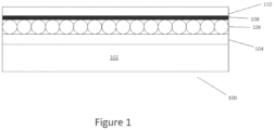
- FIG 1 a schematic cross-section of a front plane laminate (“FPL") 100 is provided.
- the FPL 100 is similar to those described in aforementioned U.S. Patent No. 6,982,178 .
- the FPL 100 comprises, in order, a light-transmissive electrically-conductive layer; a layer of a solid electro-optic medium in electrical contact with the electrically-conductive layer; an adhesive layer; and a release sheet.
- the light-transmissive electrically-conductive layer 104 is applied to a light-transmissive substrate 102, which is preferably flexible, in the sense that the substrate can be manually wrapped around a drum 10 inches (254 mm) in diameter, for example, without permanent deformation.
- the term "light-transmissive" is used herein throughout the specification and claims to mean that the layer thus designated transmits sufficient light to enable an observer, looking through that layer, to observe the change in display states of the electro-optic medium, which will normally be viewed through the electrically-conductive layer and adjacent substrate (if present); in cases where the electro-optic medium displays a change in reflectivity at non-visible wavelengths, the term “light-transmissive” should of course be interpreted to refer to transmission of the relevant non-visible wavelengths.
- the substrate 102 may be manufactured from glass or a polymeric film, for example, and may have a thickness in the range of about 1 to about 25 mil (25 to 634 ⁇ m), preferably about 2 to about 10 mil (51 to 254 ⁇ m).
- the top conductive layer 104 may comprise a thin metal or metal oxide layer of, for example, ITO, or may be a conductive polymer, such as PEDOT.
- a coating of electro-optic medium 106 is applied over the top conductive layer 104, such that the electro-optic medium 106 is in electrical contact with the top conductive layer 104.
- the electro-optic medium 106 may, preferably, be in the form of an opposite charge dual particle encapsulated electrophoretic medium of the type described in U.S. Patent Application 2002/0185378 .
- the medium may comprise dispersion media encapsulated within a binder.
- the dispersion media may contain a hydrocarbon-based liquid in which are suspended negatively charged white particles and positively charged black particles.
- the white particles may move to the positive electrode and the black particles may move to the negative electrode, for example, so that the electro-optic medium 106 appears, to an observer viewing the display through the substrate 102, white or black depending upon whether the top conductive layer 104 is positive or negative relative to the backplane at any point within the final display.
- the electro-optic medium 106 may alternatively comprise a plurality of colored particles in addition to black and/or white particles, for example, each color having a respective charge polarity and strength.
- a layer of lamination adhesive 108 is coated over the electro-optic medium layer 106, and a release layer 110 is applied over the adhesive layer 108.
- the release layer 110 may be a PET film, for example, that is approximately 7 mil in thickness, which may be provided with any appropriate release coating, for example a silicone coating.
- the presence of this lamination adhesive layer affects the electro-optic characteristics of the displays.
- the electrical conductivity of the lamination adhesive layer affects both the low temperature performance and the resolution of the display.
- the low temperature performance of the display may be improved by increasing the conductivity of the lamination adhesive layer, for example by doping the layer with tetrabutylammonium hexafluorophosphate or other materials as described in U.S. Patent Nos.
- the FPL may optionally include a thin second conductive layer, preferably of aluminum, between the release sheet 110 and the laminate adhesive 108 that may be removed with the release sheet 110.
- the second conductive layer may be used for testing of the electro-optic medium.
- the FPL may also be provided in other forms, such as a "double release sheet" as described in U.S. Patent No. 7,561,324 or an "inverted front plane laminate", as described in U. S. Patent No. 7,839,564 .
- backplanes There are three main categories of backplanes: an active matrix, a passive matrix, and a direct drive backplane. Any type of backplane may be used in the present invention in order to provide a top plane connection within the perimeter of the laminate.
- an array of thin film transistors are formed on the surface of a substrate and each transistor acts as a switch for a pixel.
- the TFT is addressed by a set of narrow multiplexed electrodes (gate lines and source lines).
- a pixel is addressed by applying voltage to a gate line that switches the TFT on and allows a charge from the source line to flow on to the rear electrode. This sets up a voltage across the pixel and turns it on.
- Passive-matrix backplanes use a simple grid to supply the charge to a particular pixel on the display.
- the grids are formed on top and bottom substrates.
- One substrate forms the “columns” and the other substrate forms the "rows”.
- the wiring of the column or rows is made from a transparent conductive material, usually indium-tin oxide (ITO).
- ITO indium-tin oxide
- the rows or columns are connected to integrated circuits that control when a charge is sent down a particular column or row.
- Assembly of an electro-optic display using FPL 100 may be effected by removing the release sheet 110 and contacting the adhesive layer 108 with a backplane under conditions effective to cause the adhesive layer 108 to adhere to the backplane, thereby securing the adhesive layer 108, layer of electro-optic medium 106 and electrically-conductive top layer 104 to the backplane, and then cut into pieces of any size needed for use with specific backplanes.
- the lamination of the FPL to the backplane may advantageously be carried out by vacuum lamination.
- Vacuum lamination is effective in expelling air from between the two materials being laminated, thus avoiding unwanted air bubbles in the final display; such air bubbles may introduce undesirable artifacts in the images produced on the display.
- vacuum lamination of the two parts of an electro-optic display in this manner imposes stringent requirements upon the lamination adhesive used, especially in the case of a display using an encapsulated electrophoretic medium.
- the lamination adhesive should have sufficient adhesive strength to bind the electro-optic layer to the backplane, and in the case of an encapsulated electrophoretic medium, the adhesive should also have sufficient adhesive strength to mechanically hold the capsules together.
- the adhesive is preferably chemically compatible with all the other materials in the display. If the electro-optic display is to be of a flexible type, the adhesive should have sufficient flexibility not to introduce defects into the display when the display is flexed.
- the lamination adhesive should have adequate flow properties at the lamination temperature to ensure high quality lamination. Furthermore, the lamination temperature is preferably as low as possible.
- An example of a useful lamination adhesive that may be incorporated in the various embodiments of the present invention an aqueous polyurethane dispersion known as a "TMXDI/PPO" dispersion, as described in U.S. Patent Application Publication No. 2005/0107564 .
- an electro-optic display is made according to a process in which an FPL is laminated to a backplane after a conductive material is applied to either a conductor located on the backplane or the adhesive layer of the FPL.
- a conductive material 1180 may first be applied to one of a plurality of conductors 1140, 1160 located on a surface of a substrate 1120 forming the backplane.
- the backplane may subsequently be laminated to an FPL comprising, in order, a light-transmissive substrate 1020 (such as PET), a light-transmissive electrically conductive layer 1040 (such as ITO), a layer of electro-optic media 1060, and a layer of lamination adhesive 1080.
- the lamination step is performed such that the conductive material 1180 penetrates through the layer of electro-optic media 1060 to provide an electrical connection between the conductor 1160 and the electrically conductive layer 1040, thereby forming a TPC.
- the conductive material 1180 contacts the electrically conductive layer 1040 and conductor 1160 after lamination. However, if the conductivity of the conductive material 1180 is sufficiently high, a conductive material 1180 in close proximity to, but not contacting, one or both of the conductive layer 1040 and conductor 1160 may still provide a TPC.
- the conductive material 1180 may alternatively be applied to the layer of lamination adhesive 1080 prior to the lamination step. However, it is preferred to apply the conductive material 1180 to the conductor 1160 located on the backplane to avoid potential misalignment of the TPC after lamination.
- the conductive material may comprises various materials known to those of skill in the art.
- the conductive material may comprise conductive particles of carbon or non-reactive metals, such as gold, and/or anisotropic epoxy conductors.
- the conductive particles preferably have a mean particle diameter of 50 microns.
- Anisotropic epoxy materials may preferably be cast into specific shapes prior to application to the backplane or FPL prior to lamination. The shapes may be designed to facilitate penetration through the layer of electro-optic media. During high temperature lamination, the epoxy may maintain enough rigidity to displace ink and adhesive, but deform as a lamination roller presses the FPL and backplane together.
- the present invention simplifies the production of custom large area displays where alignment jigs and other equipment are not available for precision aligned lamination. It also makes possible the use of roll-to-roll production of displays using continuous rolls of FPL and backplane.
- the electrical connection between the top conductive layer and the backplane will be robust and reliable due to the relatively large area of exposed top conductive layer.
- small volume orders can be made with high yield, especially in applications in which the TPC cannot be hidden behind a bezel or frame and must be small.
- the small TPC provided using the process of the invention may be highly desirable in such applications.
Landscapes
- Physics & Mathematics (AREA)
- Nonlinear Science (AREA)
- Optics & Photonics (AREA)
- General Physics & Mathematics (AREA)
- Chemical & Material Sciences (AREA)
- Chemical Kinetics & Catalysis (AREA)
- Electrochemistry (AREA)
- Molecular Biology (AREA)
- Life Sciences & Earth Sciences (AREA)
- Health & Medical Sciences (AREA)
- Mathematical Physics (AREA)
- Crystallography & Structural Chemistry (AREA)
- Electrochromic Elements, Electrophoresis, Or Variable Reflection Or Absorption Elements (AREA)
- Devices For Indicating Variable Information By Combining Individual Elements (AREA)
Claims (3)
- Procédé de formation d'un écran électro-optique (1000) comprenant :la formation d'un stratifié de face avant comprenant, dans cet ordre, un premier substrat (1020), une première couche conductrice (1040), une couche de milieu électro-optique (1060) et un adhésif (1080), le premier substrat (1020) et la première couche conductrice (1040) étant transparents ;l'obtention d'un fond de panier (1120) comprenant un conducteur (1140, 1160) situé sur une surface du fond de panier (1120) ; etl'application d'un matériau conducteur (1180) au conducteur (1160) et/ou à l'adhésif (1080) ;caractérisé en ce que le procédé comporte :
la stratification du stratifié de face avant sur le fond de panier (1120) de telle sorte que le matériau conducteur (1180) pénètre dans la couche de milieu électro-optique (1060) pour fournir une connexion électrique entre la première couche conductrice (1040) et le conducteur (1160), dans lequel le matériau conducteur (1180) touche la première couche conductrice (1040) uniquement après l'étape de stratification. - Procédé selon la revendication 1, dans lequel le matériau conducteur (1180) comprend au moins un élément parmi des particules de carbone, des métaux non réactifs, et des conducteurs en résine époxy moulés anisotropes.
- Écran électro-optique (1000) fabriqué selon le procédé de la revendication 1.
Priority Applications (1)
| Application Number | Priority Date | Filing Date | Title |
|---|---|---|---|
| EP25156913.3A EP4550042B1 (fr) | 2016-11-30 | 2017-11-15 | Affichages électro-optiques stratifiés et leurs procédés de fabrication |
Applications Claiming Priority (3)
| Application Number | Priority Date | Filing Date | Title |
|---|---|---|---|
| US201662427970P | 2016-11-30 | 2016-11-30 | |
| PCT/US2017/061710 WO2018102126A1 (fr) | 2016-11-30 | 2017-11-15 | Affichages électro-optiques stratifiés et procédés de fabrication |
| EP17875756.3A EP3548966B1 (fr) | 2016-11-30 | 2017-11-15 | Affichages électro-optiques stratifiés et procédés de fabrication |
Related Parent Applications (2)
| Application Number | Title | Priority Date | Filing Date |
|---|---|---|---|
| EP17875756.3A Division EP3548966B1 (fr) | 2016-11-30 | 2017-11-15 | Affichages électro-optiques stratifiés et procédés de fabrication |
| EP17875756.3A Division-Into EP3548966B1 (fr) | 2016-11-30 | 2017-11-15 | Affichages électro-optiques stratifiés et procédés de fabrication |
Related Child Applications (2)
| Application Number | Title | Priority Date | Filing Date |
|---|---|---|---|
| EP25156913.3A Division-Into EP4550042B1 (fr) | 2016-11-30 | 2017-11-15 | Affichages électro-optiques stratifiés et leurs procédés de fabrication |
| EP25156913.3A Division EP4550042B1 (fr) | 2016-11-30 | 2017-11-15 | Affichages électro-optiques stratifiés et leurs procédés de fabrication |
Publications (3)
| Publication Number | Publication Date |
|---|---|
| EP3992706A1 EP3992706A1 (fr) | 2022-05-04 |
| EP3992706B1 true EP3992706B1 (fr) | 2025-03-19 |
| EP3992706C0 EP3992706C0 (fr) | 2025-03-19 |
Family
ID=62190132
Family Applications (3)
| Application Number | Title | Priority Date | Filing Date |
|---|---|---|---|
| EP25156913.3A Active EP4550042B1 (fr) | 2016-11-30 | 2017-11-15 | Affichages électro-optiques stratifiés et leurs procédés de fabrication |
| EP21206101.4A Active EP3992706B1 (fr) | 2016-11-30 | 2017-11-15 | Affichages électro-optiques stratifiés et procédés de fabrication |
| EP17875756.3A Active EP3548966B1 (fr) | 2016-11-30 | 2017-11-15 | Affichages électro-optiques stratifiés et procédés de fabrication |
Family Applications Before (1)
| Application Number | Title | Priority Date | Filing Date |
|---|---|---|---|
| EP25156913.3A Active EP4550042B1 (fr) | 2016-11-30 | 2017-11-15 | Affichages électro-optiques stratifiés et leurs procédés de fabrication |
Family Applications After (1)
| Application Number | Title | Priority Date | Filing Date |
|---|---|---|---|
| EP17875756.3A Active EP3548966B1 (fr) | 2016-11-30 | 2017-11-15 | Affichages électro-optiques stratifiés et procédés de fabrication |
Country Status (9)
| Country | Link |
|---|---|
| US (3) | US10503041B2 (fr) |
| EP (3) | EP4550042B1 (fr) |
| JP (2) | JP6764038B2 (fr) |
| KR (1) | KR102308588B1 (fr) |
| CN (2) | CN109983399B (fr) |
| ES (2) | ES3020088T3 (fr) |
| PL (1) | PL3992706T3 (fr) |
| TW (2) | TWI691773B (fr) |
| WO (1) | WO2018102126A1 (fr) |
Families Citing this family (24)
| Publication number | Priority date | Publication date | Assignee | Title |
|---|---|---|---|---|
| CN107315283B (zh) * | 2017-08-17 | 2021-03-05 | 京东方科技集团股份有限公司 | 背光模组、显示装置和调节背光模组出光亮度的方法 |
| CN109870837B (zh) * | 2017-12-05 | 2021-10-15 | 华为终端有限公司 | 显示组件、显示器、终端及显示器拆卸方法 |
| KR102599722B1 (ko) * | 2018-12-28 | 2023-11-09 | 삼성디스플레이 주식회사 | 표시 패널 및 이를 포함하는 타일드 표시 장치 |
| CN113316741B (zh) * | 2019-01-21 | 2024-11-12 | 九州奈米技术光学股份有限公司 | 液晶元件的电极安装方法 |
| KR102818504B1 (ko) * | 2020-06-30 | 2025-06-10 | 엘지이노텍 주식회사 | 광 경로 제어 부재 및 이를 포함하는 디스플레이 장치 |
| KR102925199B1 (ko) * | 2020-06-30 | 2026-02-10 | 엘지이노텍 주식회사 | 광 경로 제어 부재 및 이를 포함하는 디스플레이 장치 |
| WO2022020075A1 (fr) * | 2020-07-22 | 2022-01-27 | E Ink Corporation | Dispositif électro-optique comprenant un joint d'étanchéité de bord conducteur intégré et son procédé de production |
| KR20220021966A (ko) * | 2020-08-13 | 2022-02-23 | 삼성디스플레이 주식회사 | 표시 패널, 이의 제조 방법 및 표시 패널을 포함하는 표시 장치 |
| JP7637768B2 (ja) * | 2020-10-02 | 2025-02-28 | イー インク コーポレイション | 外側表面の電気的接続を伴うフロントプレーン積層体 |
| JP7688154B2 (ja) | 2021-04-16 | 2025-06-03 | イー インク コーポレイション | 薄型縁シールを伴う電気泳動ディスプレイ |
| KR102874586B1 (ko) * | 2021-08-04 | 2025-10-21 | 이 잉크 코포레이션 | 전극 상에 유전체 코팅을 갖는 전기영동 디스플레이 |
| TWI847563B (zh) * | 2022-02-25 | 2024-07-01 | 美商電子墨水股份有限公司 | 具有邊緣密封組件的電光顯示器及其製造方法 |
| JP7839899B2 (ja) * | 2022-04-27 | 2026-04-02 | イー インク コーポレイション | セグメント化された電極を伴う電気光学ディスプレイスタックおよびそれを作る方法 |
| CN218497311U (zh) * | 2022-10-09 | 2023-02-17 | 汉朔科技股份有限公司 | 显示区域具有凹槽的电子纸屏幕 |
| TWI870787B (zh) * | 2023-02-24 | 2025-01-21 | 元太科技工業股份有限公司 | 顯示裝置 |
| US20240361618A1 (en) * | 2023-04-28 | 2024-10-31 | Gentex Corporation | Double-sided conducting films |
| US20250053058A1 (en) | 2023-08-08 | 2025-02-13 | E Ink Corporation | Backplanes for segmented electro-optic displays and methods of manufacturing same |
| US20250224645A1 (en) | 2024-01-05 | 2025-07-10 | E Ink Corporation | Electrophoretic medium comprising particles having a pigment core and a polymeric shell |
| US20250224646A1 (en) | 2024-01-08 | 2025-07-10 | E Ink Corporation | Adhesive Layer Comprising Conductive Filler Particles and a Polymeric Dispersant |
| US20250237922A1 (en) | 2024-01-19 | 2025-07-24 | E Ink Corporation | Flexible segmented electro-optic displays and methods of manufacture |
| WO2025230802A1 (fr) | 2024-04-30 | 2025-11-06 | E Ink Corporation | Dispositif de transmission de lumière variable comprenant des microcellules |
| US20250370306A1 (en) | 2024-05-30 | 2025-12-04 | E Ink Corporation | Chemically-Resistant Multi-Layered Electro-Optic Device and a Method of Making the Same |
| WO2026006119A1 (fr) | 2024-06-26 | 2026-01-02 | E Ink Corporation | Dispositif de transmission de lumière variable comprenant des microcellules |
| US20260003243A1 (en) | 2024-06-26 | 2026-01-01 | E Ink Corporation | Variable light transmission device comprising microcells |
Family Cites Families (67)
| Publication number | Priority date | Publication date | Assignee | Title |
|---|---|---|---|---|
| US55091A (en) | 1866-05-29 | Improvement in portable field-fence | ||
| US6137467A (en) | 1995-01-03 | 2000-10-24 | Xerox Corporation | Optically sensitive electric paper |
| US7411719B2 (en) | 1995-07-20 | 2008-08-12 | E Ink Corporation | Electrophoretic medium and process for the production thereof |
| US6866760B2 (en) | 1998-08-27 | 2005-03-15 | E Ink Corporation | Electrophoretic medium and process for the production thereof |
| US5760761A (en) | 1995-12-15 | 1998-06-02 | Xerox Corporation | Highlight color twisting ball display |
| US5808783A (en) | 1996-06-27 | 1998-09-15 | Xerox Corporation | High reflectance gyricon display |
| US6055091A (en) | 1996-06-27 | 2000-04-25 | Xerox Corporation | Twisting-cylinder display |
| US5777782A (en) | 1996-12-24 | 1998-07-07 | Xerox Corporation | Auxiliary optics for a twisting ball display |
| DE69830566T2 (de) | 1997-02-06 | 2006-05-11 | University College Dublin | Elektrochromes system |
| US7002728B2 (en) | 1997-08-28 | 2006-02-21 | E Ink Corporation | Electrophoretic particles, and processes for the production thereof |
| US6054071A (en) | 1998-01-28 | 2000-04-25 | Xerox Corporation | Poled electrets for gyricon-based electric-paper displays |
| US7075502B1 (en) | 1998-04-10 | 2006-07-11 | E Ink Corporation | Full color reflective display with multichromatic sub-pixels |
| US6241921B1 (en) | 1998-05-15 | 2001-06-05 | Massachusetts Institute Of Technology | Heterogeneous display elements and methods for their fabrication |
| US6128124A (en) | 1998-10-16 | 2000-10-03 | Xerox Corporation | Additive color electric paper without registration or alignment of individual elements |
| US6147791A (en) | 1998-11-25 | 2000-11-14 | Xerox Corporation | Gyricon displays utilizing rotating elements and magnetic latching |
| US6097531A (en) | 1998-11-25 | 2000-08-01 | Xerox Corporation | Method of making uniformly magnetized elements for a gyricon display |
| US6312304B1 (en) * | 1998-12-15 | 2001-11-06 | E Ink Corporation | Assembly of microencapsulated electronic displays |
| US7012600B2 (en) | 1999-04-30 | 2006-03-14 | E Ink Corporation | Methods for driving bistable electro-optic displays, and apparatus for use therein |
| US8009348B2 (en) | 1999-05-03 | 2011-08-30 | E Ink Corporation | Machine-readable displays |
| HK1047623B (en) | 1999-10-11 | 2005-05-06 | University College Dublin | Electrochromic device |
| US7715088B2 (en) | 2000-03-03 | 2010-05-11 | Sipix Imaging, Inc. | Electrophoretic display |
| ATE415644T1 (de) * | 2000-05-04 | 2008-12-15 | Schott Donnelly Llc | Verfahren zur herstellung einer electrochromen tafel |
| AU2002250304A1 (en) | 2001-03-13 | 2002-09-24 | E Ink Corporation | Apparatus for displaying drawings |
| US7679814B2 (en) | 2001-04-02 | 2010-03-16 | E Ink Corporation | Materials for use in electrophoretic displays |
| JP4188091B2 (ja) | 2001-05-15 | 2008-11-26 | イー インク コーポレイション | 電気泳動粒子 |
| US20020188053A1 (en) | 2001-06-04 | 2002-12-12 | Sipix Imaging, Inc. | Composition and process for the sealing of microcups in roll-to-roll display manufacturing |
| US6982178B2 (en) | 2002-06-10 | 2006-01-03 | E Ink Corporation | Components and methods for use in electro-optic displays |
| US7535624B2 (en) | 2001-07-09 | 2009-05-19 | E Ink Corporation | Electro-optic display and materials for use therein |
| US6950220B2 (en) | 2002-03-18 | 2005-09-27 | E Ink Corporation | Electro-optic displays, and methods for driving same |
| WO2003092077A2 (fr) | 2002-04-24 | 2003-11-06 | E Ink Corporation | Fonds de panier pour applications d'affichage |
| US7223672B2 (en) | 2002-04-24 | 2007-05-29 | E Ink Corporation | Processes for forming backplanes for electro-optic displays |
| CN101109885B (zh) | 2002-09-03 | 2012-06-13 | 伊英克公司 | 电光显示器 |
| US7839564B2 (en) | 2002-09-03 | 2010-11-23 | E Ink Corporation | Components and methods for use in electro-optic displays |
| TWI229230B (en) | 2002-10-31 | 2005-03-11 | Sipix Imaging Inc | An improved electrophoretic display and novel process for its manufacture |
| US6922276B2 (en) | 2002-12-23 | 2005-07-26 | E Ink Corporation | Flexible electro-optic displays |
| US7339715B2 (en) | 2003-03-25 | 2008-03-04 | E Ink Corporation | Processes for the production of electrophoretic displays |
| EP1616217B1 (fr) | 2003-03-27 | 2010-10-20 | E Ink Corporation | Ensembles electro-optiques |
| US7420549B2 (en) | 2003-10-08 | 2008-09-02 | E Ink Corporation | Electro-wetting displays |
| CN101382719B (zh) * | 2003-10-24 | 2012-04-04 | 伊英克公司 | 电光显示器 |
| US7173752B2 (en) | 2003-11-05 | 2007-02-06 | E Ink Corporation | Electro-optic displays, and materials for use therein |
| US7342068B2 (en) | 2003-11-18 | 2008-03-11 | Air Products And Chemicals, Inc. | Aqueous polyurethane dispersion and method for making and using same |
| US7453445B2 (en) | 2004-08-13 | 2008-11-18 | E Ink Corproation | Methods for driving electro-optic displays |
| US8576162B2 (en) | 2005-03-14 | 2013-11-05 | Sipix Imaging, Inc. | Manufacturing processes of backplane for segment displays |
| CN101371180A (zh) * | 2005-10-18 | 2009-02-18 | 伊英克公司 | 用于电光显示器的部件 |
| US8173519B2 (en) * | 2006-03-03 | 2012-05-08 | Semiconductor Energy Laboratory Co., Ltd. | Method for manufacturing semiconductor device |
| US7843624B2 (en) | 2006-03-08 | 2010-11-30 | E Ink Corporation | Electro-optic displays, and materials and methods for production thereof |
| US7733554B2 (en) | 2006-03-08 | 2010-06-08 | E Ink Corporation | Electro-optic displays, and materials and methods for production thereof |
| JP4211808B2 (ja) | 2006-06-23 | 2009-01-21 | セイコーエプソン株式会社 | 電気光学装置及び電子機器 |
| US20150005720A1 (en) | 2006-07-18 | 2015-01-01 | E Ink California, Llc | Electrophoretic display |
| TWI361331B (en) * | 2007-06-01 | 2012-04-01 | Pervasive Display Co Ltd | E-paper apparatus |
| JP5521309B2 (ja) | 2008-10-29 | 2014-06-11 | セイコーエプソン株式会社 | 電気泳動表示素子の製造方法 |
| JP2012014206A (ja) * | 2008-10-31 | 2012-01-19 | Nissha Printing Co Ltd | タッチ入力機能付き保護パネルのfpc接続方法 |
| JP2010181768A (ja) * | 2009-02-09 | 2010-08-19 | Citizen Holdings Co Ltd | 電気泳動型表示装置 |
| JP2011099948A (ja) * | 2009-11-05 | 2011-05-19 | Panasonic Corp | 電子ペーパ及び電子ペーパ書き込み装置 |
| KR101203388B1 (ko) | 2010-04-28 | 2012-11-21 | 주식회사 이미지앤머터리얼스 | 전기 광학 디스플레이 장치용 입자, 그 제조 방법 및 전기 영동 디스플레이 장치 |
| JP2012003988A (ja) * | 2010-06-17 | 2012-01-05 | Hitachi Displays Ltd | 有機エレクトロルミネッセンスパネルの製造方法 |
| JP2012119532A (ja) * | 2010-12-01 | 2012-06-21 | Seiko Epson Corp | 薄膜トランジスタ形成用基板、半導体装置、電気装置 |
| JP2012181445A (ja) * | 2011-03-02 | 2012-09-20 | Seiko Epson Corp | 電気装置 |
| WO2012128105A1 (fr) * | 2011-03-19 | 2012-09-27 | シャープ株式会社 | Élément d'affichage, appareil d'affichage et procédé d'affichage |
| JP4882031B1 (ja) * | 2011-04-26 | 2012-02-22 | 株式会社サクラクレパス | 電気泳動表示装置 |
| US10042189B2 (en) | 2011-12-01 | 2018-08-07 | Avery Dennison Retail Information Services, Llc | Backplane for electrophoretic display |
| GB201208680D0 (en) * | 2012-05-17 | 2012-06-27 | Origold As | Method of manufacturing an electronic card |
| EP2877895B1 (fr) * | 2012-07-27 | 2017-09-06 | E Ink Corporation | Processus de production d'affichages électro-optiques |
| US9279906B2 (en) | 2012-08-31 | 2016-03-08 | E Ink California, Llc | Microstructure film |
| ES2661512T3 (es) * | 2013-09-17 | 2018-04-02 | Essilor International | Composición electrocrómica |
| WO2015148398A1 (fr) | 2014-03-25 | 2015-10-01 | E Ink California, Llc | Ensemble d'affichage magnétophorétique et schéma de commande |
| CN105261163B (zh) | 2014-07-10 | 2019-02-22 | 元太科技工业股份有限公司 | 智能提醒药盒 |
-
2017
- 2017-11-03 US US15/802,571 patent/US10503041B2/en active Active
- 2017-11-15 ES ES21206101T patent/ES3020088T3/es active Active
- 2017-11-15 PL PL21206101.4T patent/PL3992706T3/pl unknown
- 2017-11-15 ES ES25156913T patent/ES3062258T3/es active Active
- 2017-11-15 WO PCT/US2017/061710 patent/WO2018102126A1/fr not_active Ceased
- 2017-11-15 EP EP25156913.3A patent/EP4550042B1/fr active Active
- 2017-11-15 EP EP21206101.4A patent/EP3992706B1/fr active Active
- 2017-11-15 KR KR1020197015079A patent/KR102308588B1/ko active Active
- 2017-11-15 JP JP2019547577A patent/JP6764038B2/ja active Active
- 2017-11-15 CN CN201780071231.3A patent/CN109983399B/zh active Active
- 2017-11-15 CN CN202210696255.0A patent/CN114995006B/zh active Active
- 2017-11-15 EP EP17875756.3A patent/EP3548966B1/fr active Active
- 2017-11-20 TW TW106140140A patent/TWI691773B/zh active
- 2017-11-20 TW TW109112615A patent/TWI754917B/zh active
-
2019
- 2019-11-06 US US16/675,620 patent/US11397362B2/en active Active
-
2020
- 2020-09-10 JP JP2020151834A patent/JP2021009394A/ja active Pending
-
2022
- 2022-02-28 US US17/682,627 patent/US11829047B2/en active Active
Also Published As
| Publication number | Publication date |
|---|---|
| WO2018102126A1 (fr) | 2018-06-07 |
| TW201825995A (zh) | 2018-07-16 |
| KR20190060889A (ko) | 2019-06-03 |
| JP2019536116A (ja) | 2019-12-12 |
| US20200073194A1 (en) | 2020-03-05 |
| EP4550042A2 (fr) | 2025-05-07 |
| EP3548966A4 (fr) | 2019-10-09 |
| KR102308588B1 (ko) | 2021-10-01 |
| US11397362B2 (en) | 2022-07-26 |
| EP4550042C0 (fr) | 2026-01-14 |
| EP3992706C0 (fr) | 2025-03-19 |
| US20220179276A1 (en) | 2022-06-09 |
| ES3062258T3 (en) | 2026-04-09 |
| PL3992706T3 (pl) | 2025-07-21 |
| CN109983399A (zh) | 2019-07-05 |
| EP3548966B1 (fr) | 2022-01-19 |
| ES3020088T3 (en) | 2025-05-21 |
| CN114995006B (zh) | 2025-11-07 |
| EP3992706A1 (fr) | 2022-05-04 |
| EP4550042B1 (fr) | 2026-01-14 |
| TWI691773B (zh) | 2020-04-21 |
| CN109983399B (zh) | 2022-07-12 |
| JP6764038B2 (ja) | 2020-09-30 |
| US11829047B2 (en) | 2023-11-28 |
| JP2021009394A (ja) | 2021-01-28 |
| US20180149942A1 (en) | 2018-05-31 |
| EP3548966A1 (fr) | 2019-10-09 |
| US10503041B2 (en) | 2019-12-10 |
| TWI754917B (zh) | 2022-02-11 |
| EP4550042A3 (fr) | 2025-07-30 |
| TW202028836A (zh) | 2020-08-01 |
| CN114995006A (zh) | 2022-09-02 |
Similar Documents
| Publication | Publication Date | Title |
|---|---|---|
| EP3992706B1 (fr) | Affichages électro-optiques stratifiés et procédés de fabrication | |
| US12038666B2 (en) | Method of forming a top plane connection in an electro-optic device | |
| US9671635B2 (en) | Electro-optic display backplane structures with drive components and pixel electrodes on opposed surfaces | |
| TWI774938B (zh) | 電光顯示器的組合體 | |
| US20250053058A1 (en) | Backplanes for segmented electro-optic displays and methods of manufacturing same | |
| US20250237922A1 (en) | Flexible segmented electro-optic displays and methods of manufacture | |
| HK40072011A (zh) | 层压电光显示器及其制造方法 | |
| HK40003820A (en) | Laminated electro-optic displays and methods of making the same | |
| HK40003820B (en) | Laminated electro-optic displays and methods of making the same | |
| HK40031048A (en) | Assemblies of electro-optic displays |
Legal Events
| Date | Code | Title | Description |
|---|---|---|---|
| PUAI | Public reference made under article 153(3) epc to a published international application that has entered the european phase |
Free format text: ORIGINAL CODE: 0009012 |
|
| STAA | Information on the status of an ep patent application or granted ep patent |
Free format text: STATUS: THE APPLICATION HAS BEEN PUBLISHED |
|
| AC | Divisional application: reference to earlier application |
Ref document number: 3548966 Country of ref document: EP Kind code of ref document: P |
|
| AK | Designated contracting states |
Kind code of ref document: A1 Designated state(s): AL AT BE BG CH CY CZ DE DK EE ES FI FR GB GR HR HU IE IS IT LI LT LU LV MC MK MT NL NO PL PT RO RS SE SI SK SM TR |
|
| STAA | Information on the status of an ep patent application or granted ep patent |
Free format text: STATUS: REQUEST FOR EXAMINATION WAS MADE |
|
| 17P | Request for examination filed |
Effective date: 20221104 |
|
| RBV | Designated contracting states (corrected) |
Designated state(s): AL AT BE BG CH CY CZ DE DK EE ES FI FR GB GR HR HU IE IS IT LI LT LU LV MC MK MT NL NO PL PT RO RS SE SI SK SM TR |
|
| GRAP | Despatch of communication of intention to grant a patent |
Free format text: ORIGINAL CODE: EPIDOSNIGR1 |
|
| STAA | Information on the status of an ep patent application or granted ep patent |
Free format text: STATUS: GRANT OF PATENT IS INTENDED |
|
| INTG | Intention to grant announced |
Effective date: 20240510 |
|
| GRAJ | Information related to disapproval of communication of intention to grant by the applicant or resumption of examination proceedings by the epo deleted |
Free format text: ORIGINAL CODE: EPIDOSDIGR1 |
|
| STAA | Information on the status of an ep patent application or granted ep patent |
Free format text: STATUS: REQUEST FOR EXAMINATION WAS MADE |
|
| INTC | Intention to grant announced (deleted) | ||
| GRAP | Despatch of communication of intention to grant a patent |
Free format text: ORIGINAL CODE: EPIDOSNIGR1 |
|
| STAA | Information on the status of an ep patent application or granted ep patent |
Free format text: STATUS: GRANT OF PATENT IS INTENDED |
|
| INTG | Intention to grant announced |
Effective date: 20241014 |
|
| GRAS | Grant fee paid |
Free format text: ORIGINAL CODE: EPIDOSNIGR3 |
|
| GRAA | (expected) grant |
Free format text: ORIGINAL CODE: 0009210 |
|
| STAA | Information on the status of an ep patent application or granted ep patent |
Free format text: STATUS: THE PATENT HAS BEEN GRANTED |
|
| AC | Divisional application: reference to earlier application |
Ref document number: 3548966 Country of ref document: EP Kind code of ref document: P |
|
| AK | Designated contracting states |
Kind code of ref document: B1 Designated state(s): AL AT BE BG CH CY CZ DE DK EE ES FI FR GB GR HR HU IE IS IT LI LT LU LV MC MK MT NL NO PL PT RO RS SE SI SK SM TR |
|
| REG | Reference to a national code |
Ref country code: GB Ref legal event code: FG4D |
|
| REG | Reference to a national code |
Ref country code: CH Ref legal event code: EP |
|
| REG | Reference to a national code |
Ref country code: DE Ref legal event code: R096 Ref document number: 602017088492 Country of ref document: DE |
|
| REG | Reference to a national code |
Ref country code: IE Ref legal event code: FG4D |
|
| U01 | Request for unitary effect filed |
Effective date: 20250403 |
|
| U07 | Unitary effect registered |
Designated state(s): AT BE BG DE DK EE FI FR IT LT LU LV MT NL PT RO SE SI Effective date: 20250409 |
|
| REG | Reference to a national code |
Ref country code: ES Ref legal event code: FG2A Ref document number: 3020088 Country of ref document: ES Kind code of ref document: T3 Effective date: 20250521 |
|
| PG25 | Lapsed in a contracting state [announced via postgrant information from national office to epo] |
Ref country code: RS Free format text: LAPSE BECAUSE OF FAILURE TO SUBMIT A TRANSLATION OF THE DESCRIPTION OR TO PAY THE FEE WITHIN THE PRESCRIBED TIME-LIMIT Effective date: 20250619 |
|
| PG25 | Lapsed in a contracting state [announced via postgrant information from national office to epo] |
Ref country code: HR Free format text: LAPSE BECAUSE OF FAILURE TO SUBMIT A TRANSLATION OF THE DESCRIPTION OR TO PAY THE FEE WITHIN THE PRESCRIBED TIME-LIMIT Effective date: 20250319 |
|
| PG25 | Lapsed in a contracting state [announced via postgrant information from national office to epo] |
Ref country code: GR Free format text: LAPSE BECAUSE OF FAILURE TO SUBMIT A TRANSLATION OF THE DESCRIPTION OR TO PAY THE FEE WITHIN THE PRESCRIBED TIME-LIMIT Effective date: 20250620 |
|
| PG25 | Lapsed in a contracting state [announced via postgrant information from national office to epo] |
Ref country code: SM Free format text: LAPSE BECAUSE OF FAILURE TO SUBMIT A TRANSLATION OF THE DESCRIPTION OR TO PAY THE FEE WITHIN THE PRESCRIBED TIME-LIMIT Effective date: 20250319 |
|
| PG25 | Lapsed in a contracting state [announced via postgrant information from national office to epo] |
Ref country code: CZ Free format text: LAPSE BECAUSE OF FAILURE TO SUBMIT A TRANSLATION OF THE DESCRIPTION OR TO PAY THE FEE WITHIN THE PRESCRIBED TIME-LIMIT Effective date: 20250319 |
|
| PG25 | Lapsed in a contracting state [announced via postgrant information from national office to epo] |
Ref country code: SK Free format text: LAPSE BECAUSE OF FAILURE TO SUBMIT A TRANSLATION OF THE DESCRIPTION OR TO PAY THE FEE WITHIN THE PRESCRIBED TIME-LIMIT Effective date: 20250319 |
|
| PG25 | Lapsed in a contracting state [announced via postgrant information from national office to epo] |
Ref country code: IS Free format text: LAPSE BECAUSE OF FAILURE TO SUBMIT A TRANSLATION OF THE DESCRIPTION OR TO PAY THE FEE WITHIN THE PRESCRIBED TIME-LIMIT Effective date: 20250719 |
|
| U20 | Renewal fee for the european patent with unitary effect paid |
Year of fee payment: 9 Effective date: 20251022 |
|
| PGFP | Annual fee paid to national office [announced via postgrant information from national office to epo] |
Ref country code: GB Payment date: 20251023 Year of fee payment: 9 |
|
| PGFP | Annual fee paid to national office [announced via postgrant information from national office to epo] |
Ref country code: NO Payment date: 20251024 Year of fee payment: 9 |
|
| PGFP | Annual fee paid to national office [announced via postgrant information from national office to epo] |
Ref country code: PL Payment date: 20251023 Year of fee payment: 9 |
|
| PLBE | No opposition filed within time limit |
Free format text: ORIGINAL CODE: 0009261 |
|
| STAA | Information on the status of an ep patent application or granted ep patent |
Free format text: STATUS: NO OPPOSITION FILED WITHIN TIME LIMIT |
|
| REG | Reference to a national code |
Ref country code: CH Ref legal event code: L10 Free format text: ST27 STATUS EVENT CODE: U-0-0-L10-L00 (AS PROVIDED BY THE NATIONAL OFFICE) Effective date: 20260128 |
|
| PGFP | Annual fee paid to national office [announced via postgrant information from national office to epo] |
Ref country code: ES Payment date: 20251201 Year of fee payment: 9 |
|
| 26N | No opposition filed |
Effective date: 20251222 |