EP3992769A1 - Procédé et appareil de stockage de données, dispositif informatique, système de stockage, et support de stockage - Google Patents
Procédé et appareil de stockage de données, dispositif informatique, système de stockage, et support de stockage Download PDFInfo
- Publication number
- EP3992769A1 EP3992769A1 EP20847721.6A EP20847721A EP3992769A1 EP 3992769 A1 EP3992769 A1 EP 3992769A1 EP 20847721 A EP20847721 A EP 20847721A EP 3992769 A1 EP3992769 A1 EP 3992769A1
- Authority
- EP
- European Patent Office
- Prior art keywords
- chunks
- chunk
- written
- stripe
- batch
- Prior art date
- Legal status (The legal status is an assumption and is not a legal conclusion. Google has not performed a legal analysis and makes no representation as to the accuracy of the status listed.)
- Granted
Links
Images


Classifications
-
- G—PHYSICS
- G06—COMPUTING OR CALCULATING; COUNTING
- G06F—ELECTRIC DIGITAL DATA PROCESSING
- G06F3/00—Input arrangements for transferring data to be processed into a form capable of being handled by the computer; Output arrangements for transferring data from processing unit to output unit, e.g. interface arrangements
- G06F3/06—Digital input from, or digital output to, record carriers, e.g. RAID, emulated record carriers or networked record carriers
- G06F3/0601—Interfaces specially adapted for storage systems
- G06F3/0628—Interfaces specially adapted for storage systems making use of a particular technique
- G06F3/0655—Vertical data movement, i.e. input-output transfer; data movement between one or more hosts and one or more storage devices
-
- G—PHYSICS
- G06—COMPUTING OR CALCULATING; COUNTING
- G06F—ELECTRIC DIGITAL DATA PROCESSING
- G06F11/00—Error detection; Error correction; Monitoring
- G06F11/07—Responding to the occurrence of a fault, e.g. fault tolerance
- G06F11/08—Error detection or correction by redundancy in data representation, e.g. by using checking codes
- G06F11/10—Adding special bits or symbols to the coded information, e.g. parity check, casting out 9's or 11's
- G06F11/1076—Parity data used in redundant arrays of independent storages, e.g. in RAID systems
-
- G—PHYSICS
- G06—COMPUTING OR CALCULATING; COUNTING
- G06F—ELECTRIC DIGITAL DATA PROCESSING
- G06F11/00—Error detection; Error correction; Monitoring
- G06F11/07—Responding to the occurrence of a fault, e.g. fault tolerance
- G06F11/08—Error detection or correction by redundancy in data representation, e.g. by using checking codes
- G06F11/10—Adding special bits or symbols to the coded information, e.g. parity check, casting out 9's or 11's
- G06F11/1008—Adding special bits or symbols to the coded information, e.g. parity check, casting out 9's or 11's in individual solid state devices
- G06F11/1068—Adding special bits or symbols to the coded information, e.g. parity check, casting out 9's or 11's in individual solid state devices in sector programmable memories, e.g. flash disk
-
- G—PHYSICS
- G06—COMPUTING OR CALCULATING; COUNTING
- G06F—ELECTRIC DIGITAL DATA PROCESSING
- G06F12/00—Accessing, addressing or allocating within memory systems or architectures
- G06F12/02—Addressing or allocation; Relocation
- G06F12/0223—User address space allocation, e.g. contiguous or non contiguous base addressing
- G06F12/023—Free address space management
- G06F12/0238—Memory management in non-volatile memory, e.g. resistive RAM or ferroelectric memory
- G06F12/0246—Memory management in non-volatile memory, e.g. resistive RAM or ferroelectric memory in block erasable memory, e.g. flash memory
-
- G—PHYSICS
- G06—COMPUTING OR CALCULATING; COUNTING
- G06F—ELECTRIC DIGITAL DATA PROCESSING
- G06F12/00—Accessing, addressing or allocating within memory systems or architectures
- G06F12/02—Addressing or allocation; Relocation
- G06F12/08—Addressing or allocation; Relocation in hierarchically structured memory systems, e.g. virtual memory systems
- G06F12/0802—Addressing of a memory level in which the access to the desired data or data block requires associative addressing means, e.g. caches
- G06F12/0866—Addressing of a memory level in which the access to the desired data or data block requires associative addressing means, e.g. caches for peripheral storage systems, e.g. disk cache
- G06F12/0868—Data transfer between cache memory and other subsystems, e.g. storage devices or host systems
-
- G—PHYSICS
- G06—COMPUTING OR CALCULATING; COUNTING
- G06F—ELECTRIC DIGITAL DATA PROCESSING
- G06F3/00—Input arrangements for transferring data to be processed into a form capable of being handled by the computer; Output arrangements for transferring data from processing unit to output unit, e.g. interface arrangements
- G06F3/06—Digital input from, or digital output to, record carriers, e.g. RAID, emulated record carriers or networked record carriers
- G06F3/0601—Interfaces specially adapted for storage systems
- G06F3/0602—Interfaces specially adapted for storage systems specifically adapted to achieve a particular effect
- G06F3/0604—Improving or facilitating administration, e.g. storage management
-
- G—PHYSICS
- G06—COMPUTING OR CALCULATING; COUNTING
- G06F—ELECTRIC DIGITAL DATA PROCESSING
- G06F3/00—Input arrangements for transferring data to be processed into a form capable of being handled by the computer; Output arrangements for transferring data from processing unit to output unit, e.g. interface arrangements
- G06F3/06—Digital input from, or digital output to, record carriers, e.g. RAID, emulated record carriers or networked record carriers
- G06F3/0601—Interfaces specially adapted for storage systems
- G06F3/0602—Interfaces specially adapted for storage systems specifically adapted to achieve a particular effect
- G06F3/0614—Improving the reliability of storage systems
- G06F3/0616—Improving the reliability of storage systems in relation to life time, e.g. increasing Mean Time Between Failures [MTBF]
-
- G—PHYSICS
- G06—COMPUTING OR CALCULATING; COUNTING
- G06F—ELECTRIC DIGITAL DATA PROCESSING
- G06F3/00—Input arrangements for transferring data to be processed into a form capable of being handled by the computer; Output arrangements for transferring data from processing unit to output unit, e.g. interface arrangements
- G06F3/06—Digital input from, or digital output to, record carriers, e.g. RAID, emulated record carriers or networked record carriers
- G06F3/0601—Interfaces specially adapted for storage systems
- G06F3/0628—Interfaces specially adapted for storage systems making use of a particular technique
- G06F3/0629—Configuration or reconfiguration of storage systems
- G06F3/0631—Configuration or reconfiguration of storage systems by allocating resources to storage systems
-
- G—PHYSICS
- G06—COMPUTING OR CALCULATING; COUNTING
- G06F—ELECTRIC DIGITAL DATA PROCESSING
- G06F3/00—Input arrangements for transferring data to be processed into a form capable of being handled by the computer; Output arrangements for transferring data from processing unit to output unit, e.g. interface arrangements
- G06F3/06—Digital input from, or digital output to, record carriers, e.g. RAID, emulated record carriers or networked record carriers
- G06F3/0601—Interfaces specially adapted for storage systems
- G06F3/0628—Interfaces specially adapted for storage systems making use of a particular technique
- G06F3/0638—Organizing or formatting or addressing of data
- G06F3/064—Management of blocks
-
- G—PHYSICS
- G06—COMPUTING OR CALCULATING; COUNTING
- G06F—ELECTRIC DIGITAL DATA PROCESSING
- G06F3/00—Input arrangements for transferring data to be processed into a form capable of being handled by the computer; Output arrangements for transferring data from processing unit to output unit, e.g. interface arrangements
- G06F3/06—Digital input from, or digital output to, record carriers, e.g. RAID, emulated record carriers or networked record carriers
- G06F3/0601—Interfaces specially adapted for storage systems
- G06F3/0668—Interfaces specially adapted for storage systems adopting a particular infrastructure
- G06F3/0671—In-line storage system
- G06F3/0673—Single storage device
- G06F3/0679—Non-volatile semiconductor memory device, e.g. flash memory, one time programmable memory [OTP]
-
- G—PHYSICS
- G06—COMPUTING OR CALCULATING; COUNTING
- G06F—ELECTRIC DIGITAL DATA PROCESSING
- G06F2212/00—Indexing scheme relating to accessing, addressing or allocation within memory systems or architectures
- G06F2212/10—Providing a specific technical effect
- G06F2212/1032—Reliability improvement, data loss prevention, degraded operation etc
- G06F2212/1036—Life time enhancement
-
- G—PHYSICS
- G06—COMPUTING OR CALCULATING; COUNTING
- G06F—ELECTRIC DIGITAL DATA PROCESSING
- G06F2212/00—Indexing scheme relating to accessing, addressing or allocation within memory systems or architectures
- G06F2212/20—Employing a main memory using a specific memory technology
- G06F2212/202—Non-volatile memory
-
- G—PHYSICS
- G06—COMPUTING OR CALCULATING; COUNTING
- G06F—ELECTRIC DIGITAL DATA PROCESSING
- G06F2212/00—Indexing scheme relating to accessing, addressing or allocation within memory systems or architectures
- G06F2212/21—Employing a record carrier using a specific recording technology
- G06F2212/214—Solid state disk
-
- G—PHYSICS
- G06—COMPUTING OR CALCULATING; COUNTING
- G06F—ELECTRIC DIGITAL DATA PROCESSING
- G06F2212/00—Indexing scheme relating to accessing, addressing or allocation within memory systems or architectures
- G06F2212/72—Details relating to flash memory management
- G06F2212/7204—Capacity control, e.g. partitioning, end-of-life degradation
-
- G—PHYSICS
- G06—COMPUTING OR CALCULATING; COUNTING
- G06F—ELECTRIC DIGITAL DATA PROCESSING
- G06F2212/00—Indexing scheme relating to accessing, addressing or allocation within memory systems or architectures
- G06F2212/72—Details relating to flash memory management
- G06F2212/7208—Multiple device management, e.g. distributing data over multiple flash devices
-
- G—PHYSICS
- G06—COMPUTING OR CALCULATING; COUNTING
- G06F—ELECTRIC DIGITAL DATA PROCESSING
- G06F3/00—Input arrangements for transferring data to be processed into a form capable of being handled by the computer; Output arrangements for transferring data from processing unit to output unit, e.g. interface arrangements
- G06F3/06—Digital input from, or digital output to, record carriers, e.g. RAID, emulated record carriers or networked record carriers
- G06F3/0601—Interfaces specially adapted for storage systems
- G06F3/0602—Interfaces specially adapted for storage systems specifically adapted to achieve a particular effect
- G06F3/0614—Improving the reliability of storage systems
- G06F3/0619—Improving the reliability of storage systems in relation to data integrity, e.g. data losses, bit errors
-
- G—PHYSICS
- G06—COMPUTING OR CALCULATING; COUNTING
- G06F—ELECTRIC DIGITAL DATA PROCESSING
- G06F3/00—Input arrangements for transferring data to be processed into a form capable of being handled by the computer; Output arrangements for transferring data from processing unit to output unit, e.g. interface arrangements
- G06F3/06—Digital input from, or digital output to, record carriers, e.g. RAID, emulated record carriers or networked record carriers
- G06F3/0601—Interfaces specially adapted for storage systems
- G06F3/0628—Interfaces specially adapted for storage systems making use of a particular technique
- G06F3/0655—Vertical data movement, i.e. input-output transfer; data movement between one or more hosts and one or more storage devices
- G06F3/0656—Data buffering arrangements
-
- G—PHYSICS
- G06—COMPUTING OR CALCULATING; COUNTING
- G06F—ELECTRIC DIGITAL DATA PROCESSING
- G06F3/00—Input arrangements for transferring data to be processed into a form capable of being handled by the computer; Output arrangements for transferring data from processing unit to output unit, e.g. interface arrangements
- G06F3/06—Digital input from, or digital output to, record carriers, e.g. RAID, emulated record carriers or networked record carriers
- G06F3/0601—Interfaces specially adapted for storage systems
- G06F3/0668—Interfaces specially adapted for storage systems adopting a particular infrastructure
- G06F3/0671—In-line storage system
- G06F3/0683—Plurality of storage devices
- G06F3/0688—Non-volatile semiconductor memory arrays
Definitions
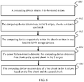
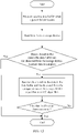
- This application provides a data storage method and apparatus, a computing device, a storage system, and a storage medium, to prevent, without relying on backup power supplies of storage devices, stripes buffered in the storage devices from getting lost when all the storage devices simultaneously have a power failure, thereby breaking a limitation that a backup power supply needs to be installed on a storage device.
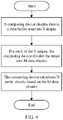
- a chunk that is in the chunks written in one batch and that is written to the storage device and a chunk that is in chunks written in a previous batch and that is written to the storage device belong to different stripes.
- the computing device 101 and the storage device 102 may provide a data storage service for the client 103.
- the client 103 may provide to-be-stored data from the computing device 101.
- the computing device 101 may obtain data from the client 103 and store the data in the storage device 102.
- the client 103 may send an input/output (input/output, I/O) request to the computing device 101, where the I/O request carries to-be-stored data; and the computing device 101 may receive the I/O request from the client 103, obtain data from the I/O request, and store the data.
- I/O input/output
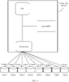
- the computing device may be the computing device 101 in the foregoing implementation environment.
- the processor 201 may be one or more central processing units (central processing unit, CPU), field-programmable gate arrays (field-programmable gate array, FPGA), application-specific integrated circuits (application-specific integrated circuit, ASIC), programmable logic devices (programmable logic device, PLD), controllers, state machines, gate logic, discrete hardware components, or any other suitable circuit.
- CPU central processing unit
- FPGA field-programmable gate array
- ASIC application-specific integrated circuit
- PLD programmable logic devices
- controllers state machines, gate logic, discrete hardware components, or any other suitable circuit.
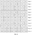
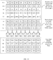
- Dij represents a data chunk at a position j of a stripe i
- Pi represents the 1 st parity chunk in the stripe i
- Qi represents the 2 nd parity chunk in the stripe i
- i is an identifier of a stripe
- i is a positive integer greater than or equal to
- j is an identifier of a chunk in the stripe
- j is a positive integer greater than or equal to 0.
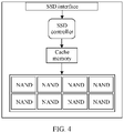
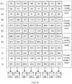
- the chunk D71 is written to the SDD 1
- the chunk D01 is written to the SDD 2
- the chunk D11 is written to the SDD 3
- the chunk D21 is written to the SDD 4
- the chunk D31 is written to the SDD 5
- the chunk D41 is written to the SDD 6
- the chunk D51 is written to the SDD 7
- the chunk D61 is written to the SDD 8.
- eight chunks in the 8 th batch are written to the eight SSDs.
- the computing device described in the embodiments of this application may alternatively be implemented by using the following: one or more field-programmable gate arrays (English full name: field-programmable gate array, English abbreviation: FPGA), a programmable logic device (English full name: programmable logic device, English abbreviation: PLD), a controller, a state machine, gate logic, a discrete hardware component, any other suitable circuit, or any combination of circuits capable of performing the various functions described throughout this application.
- field-programmable gate arrays English full name: field-programmable gate array, English abbreviation: FPGA
- a programmable logic device English full name: programmable logic device, English abbreviation: PLD
- a controller a state machine, gate logic, a discrete hardware component, any other suitable circuit, or any combination of circuits capable of performing the various functions described throughout this application.
Landscapes
- Engineering & Computer Science (AREA)
- Theoretical Computer Science (AREA)
- Physics & Mathematics (AREA)
- General Engineering & Computer Science (AREA)
- General Physics & Mathematics (AREA)
- Human Computer Interaction (AREA)
- Quality & Reliability (AREA)
- Computer Security & Cryptography (AREA)
- Techniques For Improving Reliability Of Storages (AREA)
Applications Claiming Priority (2)
| Application Number | Priority Date | Filing Date | Title |
|---|---|---|---|
| CN201910697302.1A CN110515542B (zh) | 2019-07-30 | 2019-07-30 | 数据存储方法、装置、计算设备、存储系统及存储介质 |
| PCT/CN2020/100795 WO2021017780A1 (fr) | 2019-07-30 | 2020-07-08 | Procédé et appareil de stockage de données, dispositif informatique, système de stockage, et support de stockage |
Publications (3)
| Publication Number | Publication Date |
|---|---|
| EP3992769A1 true EP3992769A1 (fr) | 2022-05-04 |
| EP3992769A4 EP3992769A4 (fr) | 2022-08-17 |
| EP3992769B1 EP3992769B1 (fr) | 2025-05-21 |
Family
ID=68624061
Family Applications (1)
| Application Number | Title | Priority Date | Filing Date |
|---|---|---|---|
| EP20847721.6A Active EP3992769B1 (fr) | 2019-07-30 | 2020-07-08 | Procédé et appareil de stockage de données, dispositif informatique, système de stockage, et support de stockage |
Country Status (4)
| Country | Link |
|---|---|
| US (1) | US11809738B2 (fr) |
| EP (1) | EP3992769B1 (fr) |
| CN (2) | CN110515542B (fr) |
| WO (1) | WO2021017780A1 (fr) |
Families Citing this family (5)
| Publication number | Priority date | Publication date | Assignee | Title |
|---|---|---|---|---|
| CN110515542B (zh) * | 2019-07-30 | 2021-08-31 | 华为技术有限公司 | 数据存储方法、装置、计算设备、存储系统及存储介质 |
| CN113467716B (zh) * | 2021-06-11 | 2023-05-23 | 苏州浪潮智能科技有限公司 | 一种数据存储的方法、装置、设备及可读介质 |
| CN114153651B (zh) * | 2022-02-09 | 2022-04-29 | 苏州浪潮智能科技有限公司 | 一种数据编码方法、装置、设备及介质 |
| CN114625576B (zh) * | 2022-05-17 | 2022-10-18 | 广州万协通信息技术有限公司 | 防掉电数据处理方法及装置 |
| CN117075821B (zh) * | 2023-10-13 | 2024-01-16 | 杭州优云科技有限公司 | 一种分布式存储方法、装置、电子设备及存储介质 |
Family Cites Families (24)
| Publication number | Priority date | Publication date | Assignee | Title |
|---|---|---|---|---|
| US20020194427A1 (en) * | 2001-06-18 | 2002-12-19 | Ebrahim Hashemi | System and method for storing data and redundancy information in independent slices of a storage device |
| US7779294B2 (en) * | 2005-04-15 | 2010-08-17 | Intel Corporation | Power-safe disk storage apparatus, systems, and methods |
| CN101166273A (zh) * | 2006-10-16 | 2008-04-23 | 华为技术有限公司 | 实现视频数据传送的方法、装置及系统 |
| US8145941B2 (en) * | 2006-10-31 | 2012-03-27 | Hewlett-Packard Development Company, L.P. | Detection and correction of block-level data corruption in fault-tolerant data-storage systems |
| US8560879B1 (en) * | 2009-04-22 | 2013-10-15 | Netapp Inc. | Data recovery for failed memory device of memory device array |
| CN101625880B (zh) * | 2009-08-14 | 2011-07-20 | 杭州华三通信技术有限公司 | 实现磁盘冗余阵列之间数据复制的控制方法和装置 |
| CN101630281B (zh) * | 2009-08-25 | 2011-11-16 | 杭州华三通信技术有限公司 | 一种数据存储的镜像方法和设备 |
| EP4361815A3 (fr) * | 2009-10-09 | 2024-06-19 | Violin Systems LLC | Système de mémoire avec bandes multiples de groupes raid et procédé pour le réaliser |
| US8417987B1 (en) * | 2009-12-01 | 2013-04-09 | Netapp, Inc. | Mechanism for correcting errors beyond the fault tolerant level of a raid array in a storage system |
| CN102521074B (zh) * | 2011-12-01 | 2013-10-16 | 浪潮电子信息产业股份有限公司 | 一种加快raid5恢复的方法 |
| GB2513377A (en) * | 2013-04-25 | 2014-10-29 | Ibm | Controlling data storage in an array of storage devices |
| CN104765693B (zh) * | 2014-01-06 | 2018-03-27 | 国际商业机器公司 | 一种用于存储数据的方法、装置和系统 |
| CN103970487A (zh) * | 2014-05-23 | 2014-08-06 | 浙江宇视科技有限公司 | 一种独立磁盘冗余阵列及实现方法 |
| CN105095013B (zh) * | 2015-06-04 | 2017-11-21 | 华为技术有限公司 | 数据存储方法、恢复方法、相关装置以及系统 |
| CN105404469B (zh) * | 2015-10-22 | 2018-11-13 | 浙江宇视科技有限公司 | 一种视频数据的存储方法和系统 |
| WO2017113276A1 (fr) | 2015-12-31 | 2017-07-06 | 华为技术有限公司 | Procédé, appareil et système de reconstruction de données dans un système de stockage distribué |
| CN109213420A (zh) * | 2017-06-29 | 2019-01-15 | 杭州海康威视数字技术股份有限公司 | 数据存储方法、装置及系统 |
| US10817376B2 (en) * | 2017-07-05 | 2020-10-27 | The Silk Technologies Ilc Ltd | RAID with heterogeneous combinations of segments |
| CN109558066B (zh) * | 2017-09-26 | 2020-10-27 | 华为技术有限公司 | 存储系统中恢复元数据的方法和装置 |
| CN108170555B (zh) * | 2017-12-21 | 2021-07-20 | 浙江大华技术股份有限公司 | 一种数据恢复方法及设备 |
| CN110018783B (zh) | 2018-01-09 | 2022-12-20 | 阿里巴巴集团控股有限公司 | 一种数据存储方法、装置及系统 |
| CN108874312B (zh) * | 2018-05-30 | 2021-09-17 | 郑州云海信息技术有限公司 | 数据存储方法以及存储设备 |
| CN109918228B (zh) * | 2019-01-28 | 2021-01-12 | 浙江中控技术股份有限公司 | 一种数据掉电保持方法及系统 |
| CN110515542B (zh) * | 2019-07-30 | 2021-08-31 | 华为技术有限公司 | 数据存储方法、装置、计算设备、存储系统及存储介质 |
-
2019
- 2019-07-30 CN CN201910697302.1A patent/CN110515542B/zh active Active
- 2019-07-30 CN CN202110857597.1A patent/CN113760186B/zh active Active
-
2020
- 2020-07-08 EP EP20847721.6A patent/EP3992769B1/fr active Active
- 2020-07-08 WO PCT/CN2020/100795 patent/WO2021017780A1/fr not_active Ceased
-
2022
- 2022-01-20 US US17/579,865 patent/US11809738B2/en active Active
Also Published As
| Publication number | Publication date |
|---|---|
| US11809738B2 (en) | 2023-11-07 |
| CN110515542A (zh) | 2019-11-29 |
| EP3992769A4 (fr) | 2022-08-17 |
| WO2021017780A1 (fr) | 2021-02-04 |
| EP3992769B1 (fr) | 2025-05-21 |
| CN113760186A (zh) | 2021-12-07 |
| CN113760186B (zh) | 2025-01-14 |
| CN110515542B (zh) | 2021-08-31 |
| US20220147268A1 (en) | 2022-05-12 |
Similar Documents
| Publication | Publication Date | Title |
|---|---|---|
| US11809738B2 (en) | Data storage method and apparatus, computing device, storage system, and storage medium | |
| CN103733175B (zh) | 一种文件处理方法、装置及存储设备 | |
| US11579974B1 (en) | Data protection using intra-device parity and intra-device parity | |
| USRE48448E1 (en) | Distributed multi-level protection in a RAID array based storage system | |
| USRE48222E1 (en) | Reconstruct reads in a raid array with dynamic geometries | |
| US10452289B1 (en) | Dynamically adjusting an amount of protection data stored in a storage system | |
| EP3373145B1 (fr) | Protection de données intradispositif dans un réseau raid | |
| CN112632643B (zh) | 防止闪存数据丢失的方法、固态硬盘控制器、固态硬盘 | |
| US11704053B1 (en) | Optimization for direct writes to raid stripes | |
| CN103718151B (zh) | 一种文件处理方法及存储设备 | |
| WO2012044489A1 (fr) | Géométries raid dynamiques dans un environnement ssd | |
| US8762771B2 (en) | Method for completing write operations to a RAID drive pool with an abnormally slow drive in a timely fashion | |
| EP2622479A1 (fr) | Protection multiniveau avec protection intra-dispositif dans une matrice raid sur la base d'un système de stockage | |
| WO2025007550A1 (fr) | Procédé de stockage de données et appareil associé | |
| CN111338846A (zh) | 一种基于多核恢复l2p表的方法和装置 | |
| US20250165156A1 (en) | Autonomous battery recharge controller |
Legal Events
| Date | Code | Title | Description |
|---|---|---|---|
| STAA | Information on the status of an ep patent application or granted ep patent |
Free format text: STATUS: THE INTERNATIONAL PUBLICATION HAS BEEN MADE |
|
| PUAI | Public reference made under article 153(3) epc to a published international application that has entered the european phase |
Free format text: ORIGINAL CODE: 0009012 |
|
| STAA | Information on the status of an ep patent application or granted ep patent |
Free format text: STATUS: REQUEST FOR EXAMINATION WAS MADE |
|
| 17P | Request for examination filed |
Effective date: 20220128 |
|
| AK | Designated contracting states |
Kind code of ref document: A1 Designated state(s): AL AT BE BG CH CY CZ DE DK EE ES FI FR GB GR HR HU IE IS IT LI LT LU LV MC MK MT NL NO PL PT RO RS SE SI SK SM TR |
|
| REG | Reference to a national code |
Ref country code: DE Ref legal event code: R079 Free format text: PREVIOUS MAIN CLASS: G06F0003060000 Ipc: G06F0011100000 Ref country code: DE Ref legal event code: R079 Ref document number: 602020051773 Country of ref document: DE Free format text: PREVIOUS MAIN CLASS: G06F0003060000 Ipc: G06F0011100000 |
|
| A4 | Supplementary search report drawn up and despatched |
Effective date: 20220714 |
|
| RIC1 | Information provided on ipc code assigned before grant |
Ipc: G06F 3/06 20060101ALI20220708BHEP Ipc: G06F 11/10 20060101AFI20220708BHEP |
|
| DAV | Request for validation of the european patent (deleted) | ||
| DAX | Request for extension of the european patent (deleted) | ||
| STAA | Information on the status of an ep patent application or granted ep patent |
Free format text: STATUS: EXAMINATION IS IN PROGRESS |
|
| 17Q | First examination report despatched |
Effective date: 20240313 |
|
| REG | Reference to a national code |
Ref country code: DE Ref legal event code: R079 Free format text: PREVIOUS MAIN CLASS: G06F0011100000 Ipc: G06F0003060000 Ref country code: DE Ref legal event code: R079 Ref document number: 602020051773 Country of ref document: DE Free format text: PREVIOUS MAIN CLASS: G06F0011100000 Ipc: G06F0003060000 |
|
| GRAP | Despatch of communication of intention to grant a patent |
Free format text: ORIGINAL CODE: EPIDOSNIGR1 |
|
| STAA | Information on the status of an ep patent application or granted ep patent |
Free format text: STATUS: GRANT OF PATENT IS INTENDED |
|
| RIC1 | Information provided on ipc code assigned before grant |
Ipc: G06F 12/02 20060101ALI20241210BHEP Ipc: G06F 11/10 20060101ALI20241210BHEP Ipc: G06F 3/06 20060101AFI20241210BHEP |
|
| INTG | Intention to grant announced |
Effective date: 20250114 |
|
| GRAS | Grant fee paid |
Free format text: ORIGINAL CODE: EPIDOSNIGR3 |
|
| GRAA | (expected) grant |
Free format text: ORIGINAL CODE: 0009210 |
|
| STAA | Information on the status of an ep patent application or granted ep patent |
Free format text: STATUS: THE PATENT HAS BEEN GRANTED |
|
| AK | Designated contracting states |
Kind code of ref document: B1 Designated state(s): AL AT BE BG CH CY CZ DE DK EE ES FI FR GB GR HR HU IE IS IT LI LT LU LV MC MK MT NL NO PL PT RO RS SE SI SK SM TR |
|
| REG | Reference to a national code |
Ref country code: GB Ref legal event code: FG4D |
|
| REG | Reference to a national code |
Ref country code: CH Ref legal event code: EP |
|
| REG | Reference to a national code |
Ref country code: DE Ref legal event code: R096 Ref document number: 602020051773 Country of ref document: DE |
|
| REG | Reference to a national code |
Ref country code: IE Ref legal event code: FG4D |
|
| REG | Reference to a national code |
Ref country code: NL Ref legal event code: MP Effective date: 20250521 |
|
| PG25 | Lapsed in a contracting state [announced via postgrant information from national office to epo] |
Ref country code: PT Free format text: LAPSE BECAUSE OF FAILURE TO SUBMIT A TRANSLATION OF THE DESCRIPTION OR TO PAY THE FEE WITHIN THE PRESCRIBED TIME-LIMIT Effective date: 20250922 Ref country code: FI Free format text: LAPSE BECAUSE OF FAILURE TO SUBMIT A TRANSLATION OF THE DESCRIPTION OR TO PAY THE FEE WITHIN THE PRESCRIBED TIME-LIMIT Effective date: 20250521 Ref country code: ES Free format text: LAPSE BECAUSE OF FAILURE TO SUBMIT A TRANSLATION OF THE DESCRIPTION OR TO PAY THE FEE WITHIN THE PRESCRIBED TIME-LIMIT Effective date: 20250521 |
|
| PGFP | Annual fee paid to national office [announced via postgrant information from national office to epo] |
Ref country code: DE Payment date: 20250604 Year of fee payment: 6 |
|
| REG | Reference to a national code |
Ref country code: LT Ref legal event code: MG9D |
|
| PG25 | Lapsed in a contracting state [announced via postgrant information from national office to epo] |
Ref country code: GR Free format text: LAPSE BECAUSE OF FAILURE TO SUBMIT A TRANSLATION OF THE DESCRIPTION OR TO PAY THE FEE WITHIN THE PRESCRIBED TIME-LIMIT Effective date: 20250822 Ref country code: NO Free format text: LAPSE BECAUSE OF FAILURE TO SUBMIT A TRANSLATION OF THE DESCRIPTION OR TO PAY THE FEE WITHIN THE PRESCRIBED TIME-LIMIT Effective date: 20250821 |
|
| PG25 | Lapsed in a contracting state [announced via postgrant information from national office to epo] |
Ref country code: NL Free format text: LAPSE BECAUSE OF FAILURE TO SUBMIT A TRANSLATION OF THE DESCRIPTION OR TO PAY THE FEE WITHIN THE PRESCRIBED TIME-LIMIT Effective date: 20250521 Ref country code: PL Free format text: LAPSE BECAUSE OF FAILURE TO SUBMIT A TRANSLATION OF THE DESCRIPTION OR TO PAY THE FEE WITHIN THE PRESCRIBED TIME-LIMIT Effective date: 20250521 |
|
| PG25 | Lapsed in a contracting state [announced via postgrant information from national office to epo] |
Ref country code: BG Free format text: LAPSE BECAUSE OF FAILURE TO SUBMIT A TRANSLATION OF THE DESCRIPTION OR TO PAY THE FEE WITHIN THE PRESCRIBED TIME-LIMIT Effective date: 20250521 |
|
| PG25 | Lapsed in a contracting state [announced via postgrant information from national office to epo] |
Ref country code: HR Free format text: LAPSE BECAUSE OF FAILURE TO SUBMIT A TRANSLATION OF THE DESCRIPTION OR TO PAY THE FEE WITHIN THE PRESCRIBED TIME-LIMIT Effective date: 20250521 |
|
| PG25 | Lapsed in a contracting state [announced via postgrant information from national office to epo] |
Ref country code: RS Free format text: LAPSE BECAUSE OF FAILURE TO SUBMIT A TRANSLATION OF THE DESCRIPTION OR TO PAY THE FEE WITHIN THE PRESCRIBED TIME-LIMIT Effective date: 20250821 |
|
| PG25 | Lapsed in a contracting state [announced via postgrant information from national office to epo] |
Ref country code: IS Free format text: LAPSE BECAUSE OF FAILURE TO SUBMIT A TRANSLATION OF THE DESCRIPTION OR TO PAY THE FEE WITHIN THE PRESCRIBED TIME-LIMIT Effective date: 20250921 |
|
| PG25 | Lapsed in a contracting state [announced via postgrant information from national office to epo] |
Ref country code: LV Free format text: LAPSE BECAUSE OF FAILURE TO SUBMIT A TRANSLATION OF THE DESCRIPTION OR TO PAY THE FEE WITHIN THE PRESCRIBED TIME-LIMIT Effective date: 20250521 |
|
| REG | Reference to a national code |
Ref country code: AT Ref legal event code: MK05 Ref document number: 1797323 Country of ref document: AT Kind code of ref document: T Effective date: 20250521 |
|
| PG25 | Lapsed in a contracting state [announced via postgrant information from national office to epo] |
Ref country code: DK Free format text: LAPSE BECAUSE OF FAILURE TO SUBMIT A TRANSLATION OF THE DESCRIPTION OR TO PAY THE FEE WITHIN THE PRESCRIBED TIME-LIMIT Effective date: 20250521 Ref country code: AT Free format text: LAPSE BECAUSE OF FAILURE TO SUBMIT A TRANSLATION OF THE DESCRIPTION OR TO PAY THE FEE WITHIN THE PRESCRIBED TIME-LIMIT Effective date: 20250521 Ref country code: SM Free format text: LAPSE BECAUSE OF FAILURE TO SUBMIT A TRANSLATION OF THE DESCRIPTION OR TO PAY THE FEE WITHIN THE PRESCRIBED TIME-LIMIT Effective date: 20250521 |
|
| PG25 | Lapsed in a contracting state [announced via postgrant information from national office to epo] |
Ref country code: CZ Free format text: LAPSE BECAUSE OF FAILURE TO SUBMIT A TRANSLATION OF THE DESCRIPTION OR TO PAY THE FEE WITHIN THE PRESCRIBED TIME-LIMIT Effective date: 20250521 |
|
| PG25 | Lapsed in a contracting state [announced via postgrant information from national office to epo] |
Ref country code: EE Free format text: LAPSE BECAUSE OF FAILURE TO SUBMIT A TRANSLATION OF THE DESCRIPTION OR TO PAY THE FEE WITHIN THE PRESCRIBED TIME-LIMIT Effective date: 20250521 |
|
| PG25 | Lapsed in a contracting state [announced via postgrant information from national office to epo] |
Ref country code: RO Free format text: LAPSE BECAUSE OF FAILURE TO SUBMIT A TRANSLATION OF THE DESCRIPTION OR TO PAY THE FEE WITHIN THE PRESCRIBED TIME-LIMIT Effective date: 20250521 Ref country code: SK Free format text: LAPSE BECAUSE OF FAILURE TO SUBMIT A TRANSLATION OF THE DESCRIPTION OR TO PAY THE FEE WITHIN THE PRESCRIBED TIME-LIMIT Effective date: 20250521 |
|
| PG25 | Lapsed in a contracting state [announced via postgrant information from national office to epo] |
Ref country code: IT Free format text: LAPSE BECAUSE OF FAILURE TO SUBMIT A TRANSLATION OF THE DESCRIPTION OR TO PAY THE FEE WITHIN THE PRESCRIBED TIME-LIMIT Effective date: 20250521 |
|
| REG | Reference to a national code |
Ref country code: CH Ref legal event code: H13 Free format text: ST27 STATUS EVENT CODE: U-0-0-H10-H13 (AS PROVIDED BY THE NATIONAL OFFICE) Effective date: 20260224 Ref country code: DE Ref legal event code: R097 Ref document number: 602020051773 Country of ref document: DE |
|
| PG25 | Lapsed in a contracting state [announced via postgrant information from national office to epo] |
Ref country code: LU Free format text: LAPSE BECAUSE OF NON-PAYMENT OF DUE FEES Effective date: 20250708 |
|
| REG | Reference to a national code |
Ref country code: BE Ref legal event code: MM Effective date: 20250731 |
|
| PLBE | No opposition filed within time limit |
Free format text: ORIGINAL CODE: 0009261 |
|
| STAA | Information on the status of an ep patent application or granted ep patent |
Free format text: STATUS: NO OPPOSITION FILED WITHIN TIME LIMIT |
|
| REG | Reference to a national code |
Ref country code: CH Ref legal event code: L10 Free format text: ST27 STATUS EVENT CODE: U-0-0-L10-L00 (AS PROVIDED BY THE NATIONAL OFFICE) Effective date: 20260402 |
|
| PG25 | Lapsed in a contracting state [announced via postgrant information from national office to epo] |
Ref country code: BE Free format text: LAPSE BECAUSE OF NON-PAYMENT OF DUE FEES Effective date: 20250731 |
|
| PG25 | Lapsed in a contracting state [announced via postgrant information from national office to epo] |
Ref country code: FR Free format text: LAPSE BECAUSE OF NON-PAYMENT OF DUE FEES Effective date: 20250721 |
|
| PG25 | Lapsed in a contracting state [announced via postgrant information from national office to epo] |
Ref country code: CH Free format text: LAPSE BECAUSE OF NON-PAYMENT OF DUE FEES Effective date: 20250731 |
|
| 26N | No opposition filed |
Effective date: 20260224 |