EP3993052B1 - Sensor und elektronische vorrichtung - Google Patents
Sensor und elektronische vorrichtung Download PDFInfo
- Publication number
- EP3993052B1 EP3993052B1 EP21204420.0A EP21204420A EP3993052B1 EP 3993052 B1 EP3993052 B1 EP 3993052B1 EP 21204420 A EP21204420 A EP 21204420A EP 3993052 B1 EP3993052 B1 EP 3993052B1
- Authority
- EP
- European Patent Office
- Prior art keywords
- sensor
- photoelectric conversion
- substituted
- unsubstituted
- conversion layer
- Prior art date
- Legal status (The legal status is an assumption and is not a legal conclusion. Google has not performed a legal analysis and makes no representation as to the accuracy of the status listed.)
- Active
Links
Images





Classifications
-
- H—ELECTRICITY
- H10—SEMICONDUCTOR DEVICES; ELECTRIC SOLID-STATE DEVICES NOT OTHERWISE PROVIDED FOR
- H10K—ORGANIC ELECTRIC SOLID-STATE DEVICES
- H10K39/00—Integrated devices, or assemblies of multiple devices, comprising at least one organic radiation-sensitive element covered by group H10K30/00
- H10K39/30—Devices controlled by radiation
- H10K39/32—Organic image sensors
-
- H—ELECTRICITY
- H10—SEMICONDUCTOR DEVICES; ELECTRIC SOLID-STATE DEVICES NOT OTHERWISE PROVIDED FOR
- H10K—ORGANIC ELECTRIC SOLID-STATE DEVICES
- H10K30/00—Organic devices sensitive to infrared radiation, light, electromagnetic radiation of shorter wavelength or corpuscular radiation
- H10K30/30—Organic devices sensitive to infrared radiation, light, electromagnetic radiation of shorter wavelength or corpuscular radiation comprising bulk heterojunctions, e.g. interpenetrating networks of donor and acceptor material domains
-
- H—ELECTRICITY
- H10—SEMICONDUCTOR DEVICES; ELECTRIC SOLID-STATE DEVICES NOT OTHERWISE PROVIDED FOR
- H10K—ORGANIC ELECTRIC SOLID-STATE DEVICES
- H10K30/00—Organic devices sensitive to infrared radiation, light, electromagnetic radiation of shorter wavelength or corpuscular radiation
- H10K30/80—Constructional details
- H10K30/81—Electrodes
-
- H—ELECTRICITY
- H10—SEMICONDUCTOR DEVICES; ELECTRIC SOLID-STATE DEVICES NOT OTHERWISE PROVIDED FOR
- H10K—ORGANIC ELECTRIC SOLID-STATE DEVICES
- H10K85/00—Organic materials used in the body or electrodes of devices covered by this subclass
- H10K85/60—Organic compounds having low molecular weight
- H10K85/615—Polycyclic condensed aromatic hydrocarbons, e.g. anthracene
- H10K85/624—Polycyclic condensed aromatic hydrocarbons, e.g. anthracene containing six or more rings
-
- H—ELECTRICITY
- H10—SEMICONDUCTOR DEVICES; ELECTRIC SOLID-STATE DEVICES NOT OTHERWISE PROVIDED FOR
- H10K—ORGANIC ELECTRIC SOLID-STATE DEVICES
- H10K85/00—Organic materials used in the body or electrodes of devices covered by this subclass
- H10K85/60—Organic compounds having low molecular weight
- H10K85/631—Amine compounds having at least two aryl rest on at least one amine-nitrogen atom, e.g. triphenylamine
- H10K85/633—Amine compounds having at least two aryl rest on at least one amine-nitrogen atom, e.g. triphenylamine comprising polycyclic condensed aromatic hydrocarbons as substituents on the nitrogen atom
-
- H—ELECTRICITY
- H10—SEMICONDUCTOR DEVICES; ELECTRIC SOLID-STATE DEVICES NOT OTHERWISE PROVIDED FOR
- H10K—ORGANIC ELECTRIC SOLID-STATE DEVICES
- H10K85/00—Organic materials used in the body or electrodes of devices covered by this subclass
- H10K85/60—Organic compounds having low molecular weight
- H10K85/649—Aromatic compounds comprising a hetero atom
- H10K85/657—Polycyclic condensed heteroaromatic hydrocarbons
- H10K85/6572—Polycyclic condensed heteroaromatic hydrocarbons comprising only nitrogen in the heteroaromatic polycondensed ring system, e.g. phenanthroline or carbazole
-
- H—ELECTRICITY
- H10—SEMICONDUCTOR DEVICES; ELECTRIC SOLID-STATE DEVICES NOT OTHERWISE PROVIDED FOR
- H10K—ORGANIC ELECTRIC SOLID-STATE DEVICES
- H10K2101/00—Properties of the organic materials covered by group H10K85/00
- H10K2101/30—Highest occupied molecular orbital [HOMO], lowest unoccupied molecular orbital [LUMO] or Fermi energy values
-
- H—ELECTRICITY
- H10—SEMICONDUCTOR DEVICES; ELECTRIC SOLID-STATE DEVICES NOT OTHERWISE PROVIDED FOR
- H10K—ORGANIC ELECTRIC SOLID-STATE DEVICES
- H10K2101/00—Properties of the organic materials covered by group H10K85/00
- H10K2101/40—Interrelation of parameters between multiple constituent active layers or sublayers, e.g. HOMO values in adjacent layers
-
- H—ELECTRICITY
- H10—SEMICONDUCTOR DEVICES; ELECTRIC SOLID-STATE DEVICES NOT OTHERWISE PROVIDED FOR
- H10K—ORGANIC ELECTRIC SOLID-STATE DEVICES
- H10K30/00—Organic devices sensitive to infrared radiation, light, electromagnetic radiation of shorter wavelength or corpuscular radiation
- H10K30/10—Organic devices sensitive to infrared radiation, light, electromagnetic radiation of shorter wavelength or corpuscular radiation comprising heterojunctions between organic semiconductors and inorganic semiconductors
-
- H—ELECTRICITY
- H10—SEMICONDUCTOR DEVICES; ELECTRIC SOLID-STATE DEVICES NOT OTHERWISE PROVIDED FOR
- H10K—ORGANIC ELECTRIC SOLID-STATE DEVICES
- H10K30/00—Organic devices sensitive to infrared radiation, light, electromagnetic radiation of shorter wavelength or corpuscular radiation
- H10K30/20—Organic devices sensitive to infrared radiation, light, electromagnetic radiation of shorter wavelength or corpuscular radiation comprising organic-organic junctions, e.g. donor-acceptor junctions
-
- H—ELECTRICITY
- H10—SEMICONDUCTOR DEVICES; ELECTRIC SOLID-STATE DEVICES NOT OTHERWISE PROVIDED FOR
- H10K—ORGANIC ELECTRIC SOLID-STATE DEVICES
- H10K50/00—Organic light-emitting devices
- H10K50/10—OLEDs or polymer light-emitting diodes [PLED]
- H10K50/11—OLEDs or polymer light-emitting diodes [PLED] characterised by the electroluminescent [EL] layers
-
- H—ELECTRICITY
- H10—SEMICONDUCTOR DEVICES; ELECTRIC SOLID-STATE DEVICES NOT OTHERWISE PROVIDED FOR
- H10K—ORGANIC ELECTRIC SOLID-STATE DEVICES
- H10K85/00—Organic materials used in the body or electrodes of devices covered by this subclass
- H10K85/20—Carbon compounds, e.g. carbon nanotubes or fullerenes
- H10K85/211—Fullerenes, e.g. C60
-
- H—ELECTRICITY
- H10—SEMICONDUCTOR DEVICES; ELECTRIC SOLID-STATE DEVICES NOT OTHERWISE PROVIDED FOR
- H10K—ORGANIC ELECTRIC SOLID-STATE DEVICES
- H10K85/00—Organic materials used in the body or electrodes of devices covered by this subclass
- H10K85/30—Coordination compounds
- H10K85/311—Phthalocyanine
-
- Y—GENERAL TAGGING OF NEW TECHNOLOGICAL DEVELOPMENTS; GENERAL TAGGING OF CROSS-SECTIONAL TECHNOLOGIES SPANNING OVER SEVERAL SECTIONS OF THE IPC; TECHNICAL SUBJECTS COVERED BY FORMER USPC CROSS-REFERENCE ART COLLECTIONS [XRACs] AND DIGESTS
- Y02—TECHNOLOGIES OR APPLICATIONS FOR MITIGATION OR ADAPTATION AGAINST CLIMATE CHANGE
- Y02E—REDUCTION OF GREENHOUSE GAS [GHG] EMISSIONS, RELATED TO ENERGY GENERATION, TRANSMISSION OR DISTRIBUTION
- Y02E10/00—Energy generation through renewable energy sources
- Y02E10/50—Photovoltaic [PV] energy
- Y02E10/549—Organic PV cells
Definitions
- An imaging device is used in a digital camera and a camcorder or the like to take (e.g., capture, generate, etc.) an image and to store the same as an electrical signal, and the imaging device includes a sensor separating incident light according to a wavelength and converting each component to an electrical signal.
- US 2019/0214591 discloses a photoelectric device including a first electrode and a second electrode facing each other and a photoelectric conversion layer between the first electrode and the second electrode and configured to convert light in a particular wavelength spectrum of light of a visible wavelength spectrum of light into an electric signal.
- the senor may include an infrared sensor that has improved sensitivity in a low illumination environment and/or may be suitable for use as a biometric or authentication device.
- Some example embodiments provide an electronic device including the sensor.
- a sensor is provided in accordance with claim 1.
- a difference between a HOMO energy level of the first material and a HOMO energy level of the third material may be less than 1.0 eV.
- a difference between a HOMO energy level of the second material and a HOMO energy level of the first material may be greater than or equal to 0.5 eV.
- the energy band gap of the first material may be 0.5 eV to 1.8 eV, and the energy band gap of the third material may be 2.8 eV to 4.0 eV.
- the energy band gap of the third material may be greater than an energy band gap of the second material.
- the first material may be included in the infrared photoelectric conversion layer in a smaller amount than the second material.
- a composition ratio of the first material to the second material in the infrared photoelectric conversion layer may be 0.10:1 to 0.90:1.
- a composition ratio of the first material to the second material in the infrared photoelectric conversion layer may be 0.10:1 to 0.50:1.
- Each of the first material and the third material may be included in the infrared photoelectric conversion layer in a smaller amount than the second material.
- the third material may be included in the infrared photoelectric conversion layer in an amount of 1 volume% to 40 volume% based on a total volume of the infrared photoelectric conversion layer.
- the third material may be included in the infrared photoelectric conversion layer in an amount of 7 volume% to 25 volume% based on a total volume of the infrared photoelectric conversion layer.
- a maximum absorption wavelength of the infrared photoelectric conversion layer may be longer than the maximum absorption wavelength of the first material.
- a maximum absorption wavelength or a maximum external quantum efficiency wavelength of the sensor may be shifted toward a longer wavelength as a content of the third material in the infrared photoelectric conversion layer increases.
- the third material may be represented by Chemical Formula 1.
- the third material may be represented by one of Chemical Formulas 1-1 to 1-8.
- the infrared photoelectric conversion layer may be a ternary system of the first material, the second material, and the third material.
- the sensor may have a maximum external quantum efficiency wavelength that is in a range of 800 nm to 1500 nm.
- the sensor may further include a first auxiliary layer between the first electrode and the infrared photoelectric conversion layer.
- the first auxiliary layer may include a fourth material, the fourth material being the same as or different from the third material.
- the energy band gap of the fourth material may be greater than the energy band gap of the first material by greater than or equal to 1.0 eV.
- a HOMO energy level of the fourth material may be between a work function of the first electrode and a HOMO energy level of the first material.
- a sensor is provided in accordance with claim 8.
- the maximum absorption wavelength of the infrared photoelectric conversion layer may be longer than the maximum absorption wavelength of the first material by greater than or equal to 30 nm.
- a maximum absorption wavelength or a maximum external quantum efficiency wavelength of the sensor may be shifted toward a longer wavelength as a content of the third material in the infrared photoelectric conversion layer increases.
- the third material may be included in the infrared photoelectric conversion layer in an amount of 1 volume% to 40 volume% based on a total volume of the infrared photoelectric conversion layer.
- the third material may be included in the infrared photoelectric conversion layer in an amount of 7 volume% to 25 volume% based on a total volume of the infrared photoelectric conversion layer.
- the maximum absorption wavelength of the first material may belong to 750 nm to 1200 nm, and the maximum absorption wavelength of the infrared photoelectric conversion layer may belong to 1000 nm to 1500 nm.
- the third material may be represented by one of Chemical Formulas 1-1 to 1-8.
- the first material may include a metal phthalocyanine complex or a metal naphthalocyanine complex.
- an electronic device including the sensor is provided.
- a HOMO energy level of the first material may be in a range of about 4.5 eV to about 5.5 eV.
- a HOMO energy level of the second material may be in a range of about 5.6 eV to about 7.0 eV.
- the second material may include fullerene or a fullerene derivative.
- the dark current of the sensor may be reduced and optical characteristics may be improved based on the infrared photoelectric conversion layer including the third material in combination with the first and second materials.
- elements and/or properties thereof e.g., structures, surfaces, directions, or the like
- elements and/or properties thereof which may be referred to as being "perpendicular,” “parallel,” “coplanar,” or the like with regard to other elements and/or properties thereof (e.g., structures, surfaces, directions, or the like) may be “perpendicular,” “parallel,” “coplanar,” or the like or may be “substantially perpendicular,” “substantially parallel,” “substantially coplanar,” respectively, with regard to the other elements and/or properties thereof.
- Elements and/or properties thereof that are “substantially identical” to, “substantially the same” as or “substantially equal” to other elements and/or properties thereof will be understood to include elements and/or properties thereof that are identical to, the same as, or equal to the other elements and/or properties thereof within manufacturing tolerances and/or material tolerances.
- Elements and/or properties thereof that are identical or substantially identical to and/or the same or substantially the same as other elements and/or properties thereof may be structurally the same or substantially the same, functionally the same or substantially the same, and/or compositionally the same or substantially the same.
- substituted refers to replacement of hydrogen of a compound or a group by a substituent selected from a halogen, a hydroxy group, a nitro group, a cyano group, an amino group, an azido group, an amidino group, a hydrazino group, a hydrazono group, a carbonyl group, a carbamyl group, a thiol group, ester group, a carboxyl group or a salt thereof, a sulfonic acid group or a salt thereof, a phosphoric acid group or a salt thereof, a silyl group, a C1 to C20 alkyl group, a C2 to C20 alkenyl group, a C2 to C20 alkynyl group, a C6 to C30 aryl group, a C7 to C30 arylalkyl group, a C1 to C30 alkoxy
- hetero refers to one including 1 to 4 heteroatoms selected from N, O, S, Se, Te, Si, and P.
- aryl group refers to a group including at least one aromatic hydrocarbon moiety. All ring-forming atoms of the aromatic hydrocarbon moiety have p-orbitals which form conjugation, for example a phenyl group, a naphthyl group, and the like; two or more aromatic hydrocarbon moieties may be linked by a sigma bond, for example a biphenyl group, a terphenyl group, a quarterphenyl group, and the like; and two or more aromatic hydrocarbon moieties may be fused directly or indirectly to provide a nonaromatic fused ring, for example a fluorenyl group.
- the aryl group may include a monocyclic, polycyclic or fused ring polycyclic (i.e., rings sharing adjacent pairs of carbon atoms) functional group.
- heterocycle or “heterocyclic group” is a generic concept of a heteroaryl group, and may be a ring including at least one heteroatom selected from N, O, S, Se, Te, P, and Si instead of carbon (C) in the ring.
- heterocycle or heterocyclic group is a fused ring, the entire ring or each ring of the heterocyclic group may include one or more heteroatoms.
- a work function, a HOMO energy level, or a LUMO energy level is expressed as an absolute value from a vacuum level.
- the work function, HOMO energy level, or LUMO energy level is referred to be deep, high, or large, it may have a large absolute value based on "0 eV" of the vacuum level, while when the work function, HOMO energy level, or LUMO energy level is referred to be shallow, low, or small, it may have a small absolute value based on "0 eV" of the vacuum level.
- the HOMO energy level is obtained by measuring a film formed of the material at room temperature using a photoelectron spectroscopy device (RIKEN KEIKI Co. Ltd., AC-3).
- RIKEN KEIKI Co. Ltd., AC-3 a photoelectron spectroscopy device
- UPS ultraviolet-visible spectrophotometer
- the energy band gap is extracted, and a value obtained by subtracting the previously measured HOMO energy level from the energy band gap is defined as the LUMO energy level.
- an energy band gap refers to an absolute value of a difference between the HOMO energy level and LUMO energy level
- the wide or large energy band gap means that an absolute value of the difference between the HOMO energy level and LUMO energy level is large.
- maximum absorption wavelength the wavelength at the point where the light absorption is maximum in the optical absorption spectrum
- EQE spectrum the wavelength at the point where the external quantum efficiency (EQE) is maximum in the external quantum efficiency spectrum
- the maximum external quantum efficiency wavelength or the maximum EQE wavelength may be the same as the maximum absorption wavelength, and the term "the maximum external quantum efficiency wavelength” (or “the maximum EQE wavelength") and “the maximum absorption wavelength” may be used interchangeably.
- non-polymeric material may be an organic material having no repeating units, and may be, for example, an organic material having a molecular weight of less than or equal to about 3000 g/mol, less than or equal to about 2500 g/mol, less than or equal to about 2000 g/mol, or less than or equal to about 1500 g/mol.
- the "non-polymeric material” may be a low molecular weight compound having a molecular weight within the above range.
- a sensor includes a sensor (hereinafter referred to as an "infrared sensor") configured to sense light in at least a portion of the infrared wavelength spectrum.
- the infrared sensor may be, for example, a sensor configured to sense light in at least a portion of a near infrared wavelength spectrum, a short wave infrared wavelength spectrum, a mid- wave infrared wavelength spectrum, and a long-wave infrared wavelength spectrum.
- the infrared sensor may be a sensor configured to sense light in at least a portion of a near infrared wavelength spectrum to a short wave infrared wavelength spectrum.
- the infrared wavelength spectrum may, for example, belong to greater than about 700 nm and less than or equal to about 3000 nm, and within this range, it may, for example, belong to about 750 nm to about 3000 nm, about 750 nm to about 2500 nm, about 750 nm to about 2300 nm, about 750 nm to about 2000 nm, about 750 nm to about 1800 nm, about 750 nm to about 1500 nm, about 750 nm to about 1300 nm, about 750 nm to about 1200 nm, about 750 nm to about 1100 nm, about 750 nm to about 1000 nm, about 800 nm to about 3000 nm, about 800 nm to about 2500 nm, about 800 nm to about 2300 nm, about 800 nm to about 2000 nm, about 800 nm to about 1800 nm, about 800 nm to about 1500
- the infrared sensor may be configured to selectively absorb light in the wavelength spectrum and convert the absorbed light into an electrical signal.
- the external quantum efficiency (EQE) spectrum of the infrared sensor may have a maximum EQE wavelength in the wavelength spectrum.
- Each infrared sensor may independently include a photo-sensing device such as a photodiode or a photoelectric conversion device.
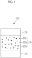
- FIG. 1 is a cross-sectional view illustrating an example of an infrared sensor according to some example embodiments.
- an infrared light sensor 100 includes a first electrode 110 and a second electrode 120 facing each other, and an infrared photoelectric conversion layer 130 between the first electrode 110 and the second electrode 120.
- An infrared sensor as described herein may be referred to as, or may be included in, a sensor.
- the substrate may be disposed under the first electrode 110 or may be disposed on the second electrode 120 and may be in direct contact with at least one of the first electrode 110 or the second electrode 120.
- the substrate may be, for example, made of an inorganic material such as glass, an organic material such as polycarbonate, polymethyl methacrylate, polyethylene terephthalate, polyethylene naphthalate, polyamide, polyethersulfone, or a combination thereof, or a silicon wafer.
- the substrate may be omitted.
- first electrode 110 or the second electrode 120 is an anode and the other is a cathode.
- first electrode 110 may be an anode
- second electrode 120 may be a cathode.
- first electrode 110 may be a cathode
- second electrode 120 may be an anode.
- At least one of the first electrode 110 or the second electrode 120 may be a transparent electrode or a semi-transmissive electrode.
- the transparent electrode may have a transmittance of greater than or equal to about 80%, and within the above range, greater than or equal to about 85%, greater than or equal to about 88%, greater than or equal to about 90%, greater than or equal to about 92%, greater than or equal to about 95%, or greater than or equal to about 97%.
- the transparent electrode may include, for example, at least one of an oxide conductor, a carbon conductor, and/or a metal thin film.
- the oxide conductor may be for example one or more selected from indium tin oxide (ITO), indium zinc oxide (IZO), zinc tin oxide (ZTO), aluminum tin oxide (AlTO), and aluminum zinc oxide (AZO).
- the carbon conductor may be one or more selected from graphene and carbon nanostructure.
- the metal thin film may be for example formed with a thin thickness of several nanometers to several tens of nanometer thickness or may be a single layer or multiple layers of metal thin film formed with a thin thickness of several nanometers to tens of nanometer thickness and doped with metal oxide.
- the semi-transmissive electrode may have a transmittance of about 10% to about 70%, about 20% to about 60%, or about 30% to about 50%, for example, selectively transmitting light in a particular (or, alternatively, predetermined) wavelength range and reflecting or absorbing light in other wavelength ranges.
- the semi-transmissive electrode may include a thin metal layer or alloy layer of, for example, about 1 nm to about 50 nm, and may include silver (Ag), copper (Cu), aluminum (Al), magnesium (Mg), ytterbium (Yb), magnesium-silver (Mg-Ag), magnesium-aluminum (Mg-Al), or a combination thereof, but the present inventive concepts are not limited thereto.
- the reflective electrode may include a reflective layer and may have a low transmittance of, for example, less than about 10% or less than or equal to about 5%.
- the light transmittance of the reflective electrode may be equal to or greater than 0%, equal to or greater than about 0.1%, equal to or greater than about 0.5%, equal to or greater than about 1%, or equal to or greater than about 5%.
- the reflective electrode may have a reflectance of greater than or equal to about 10%, greater than or equal to about 20%, greater than or equal to about 30%, greater than or equal to about 50%, or greater than or equal to about 70%.
- the reflectance of the reflective electrode may be equal to or less than 100%, equal to or less than about 99%, equal to or less than about 95%, equal to or less than about 90%, or equal to or less than about 80%.
- the reflective electrode may include a reflective conductor such as a metal, for example, silver (Ag), copper (Cu), aluminum (Al), gold (Au), titanium (Ti), chromium (Cr), nickel (Ni), ytterbium (Yb), an alloy thereof, a nitride thereof (e.g., TiN), or a combination thereof, but is not limited thereto.
- the first electrode 110 and the second electrode 120 may be a transparent electrode or a semi-transmissive electrode, respectively.
- the first electrode 110 may be a reflective electrode and the second electrode 120 may be a transparent electrode or a semi-transmissive electrode.
- the first electrode 110 may be a transparent electrode or a semi-transmissive electrode, and the second electrode 120 may be a reflective electrode.
- the infrared photoelectric conversion layer 130 may be configured to absorb light (e.g., incident light) in at least a portion of the infrared wavelength spectrum and convert the absorbed light into an electrical signal. Such absorbing and photoelectric conversion of light in an infrared wavelength spectrum may be referred to herein as "sensing" and/or "detecting" said light in the infrared wavelength spectrum.
- the absorption spectrum of the infrared photoelectric conversion layer 130 may have, for example, a maximum absorption wavelength ( ⁇ max,A ) in a wavelength spectrum of greater than about 700 nm and less than or equal to about 3000 nm.
- the maximum absorption wavelength may belong to a wavelength spectrum of, for example, about 750 nm to about 3000 nm, about 750 nm to about 2500 nm, about 750 nm to about 2300 nm, about 750 nm to about 2000 nm, about 750 nm to about 1800 nm, about 750 nm to about 1500 nm, about 750 nm to about 1300 nm, about 750 nm to about 1200 nm, about 750 nm to about 1100 nm, about 1000 nm to about 1500 nm, or about 750 nm to about 1000 nm.
- the EQE spectrum of the infrared light sensor 100 may have a maximum EQE wavelength in a wavelength range of, for example, greater than about 700 nm and less than or equal to about 3000 nm.
- the maximum EQE wavelength may belong to a wavelength spectrum of, for example, about 800 nm to about 1500 nm, about 750 nm to about 3000 nm, about 750 nm to about 2500 nm, about 750 nm to about 2300 nm, about 750 nm to about 2000 nm, about 750 nm to about 1800 nm, about 750 nm to about 1500 nm, about 750 nm to about 1300 nm, about 750 nm to about 1200 nm, about 750 nm to about 1100 nm, or about 750 nm to about 1000 nm.
- the infrared photoelectric conversion layer 130 includes at least one first material 130a and at least one second material 130b which form a pn junction (e.g., the second material 130b forms a pn junction with the first material 130a).
- the first material 130a and the second material 130b are different from each other, and one of the first material 130a or the second material 130b may be a p-type semiconductor and the other may be an n-type semiconductor.
- the first material 130a may be a p-type semiconductor and the second material 130b may be an n-type semiconductor.
- the first material 130a may be an n-type semiconductor and the second material 130b may be a p-type semiconductor.
- Each of the first material 130a and the second material 130b may be an organic material, an inorganic material, or an organic-inorganic material.
- at least one of the first material 130a or the second material 130b may be an organic material.
- the first material 130a and the second material 130b are each a non-polymeric material and may be a depositable compound.
- At least one of the first material 130a or the second material 130b may be a light absorbing material.
- the first material 130a and the second material 130b may be light absorbing materials, respectively.
- the first material 130a and the second material 130b may have different light absorption characteristics.
- the absorption spectrum of the first material 130a and the absorption spectrum of the second material 130b may be different.
- the maximum absorption wavelength of the absorption spectrum of the first material 130a and the maximum absorption wavelength of the absorption spectrum of the second material 130b may be different from each other.
- the absorption spectrum of the first material 130a may be in a longer wavelength spectrum than the absorption spectrum of the second material 130b.
- the maximum absorption wavelength of the absorption spectrum of the first material 130a may be longer than the maximum absorption wavelength of the absorption spectrum of the second material 130b.
- the first material 130a is an infrared absorbing material configured to mainly absorb light in the infrared wavelength spectrum, and the maximum absorption wavelength of the absorption spectrum of the first material 130a belongs to (e.g., may be in) the infrared wavelength spectrum.
- the maximum absorption wavelength of the absorption spectrum of the first material 130a may belong to, for example, greater than about 700 nm and less than or equal to about 3000 nm, and within the above range, for example about 750 nm to about 3000 nm, about 750 nm to about 2500 nm, about 750 nm to about 2300 nm, about 750 nm to about 2000 nm, about 750 nm to about 1800 nm, about 750 nm to about 1500 nm, about 750 nm to about 1300 nm, about 750 nm to about 1200 nm, about 750 nm to about 1100 nm, about 750 nm to about 1000 nm, about 800 nm to about 3000 nm, about 800 nm to about 2500 nm, about 800 nm to about 2300 nm, about 800 nm to about 2000 nm, about 800 nm to about 1800 nm, about 800 n
- the second material 130b may not be an infrared absorbing material configured to mainly absorb light in the infrared wavelength spectrum, and for example, the maximum absorption wavelength of the absorption spectrum of the second material 130b may not belong to the infrared wavelength spectrum.
- the second material 130b may be a visible light absorbing material configured to mainly absorb light in the visible light wavelength spectrum, and the maximum absorption wavelength of the absorption spectrum of the second material 130b may belong to the visible light wavelength spectrum.
- the visible light wavelength spectrum may be, for example, greater than or equal to about 380 nm and less than about 700 nm, and within the above range, for example, about 380 nm to about 680 nm.
- the first material 130a and the second material 130b may have different electrical properties.
- the energy diagram of the first material 130a and the energy diagram of the second material 130b may be different.
- the first material 130a may have a relatively shallow HOMO energy level.
- the HOMO energy level of the first material 130a may be about 4.5 eV to about 5.5 eV.
- the HOMO energy level of the second material 130b may be deeper than the HOMO energy level of the first material 130a, for example, a difference between the HOMO energy level of the second material 130b and the HOMO energy level of the first material 130a may be greater than or equal to about 0.5 eV, and within the above range, greater than or equal to about 0.7 eV, greater than or equal to about 0.8 eV, greater than or equal to about 0.9 eV, or greater than or equal to about 1.0 eV, for example, about 0.5 eV to about 2.0 eV, about 0.5 eV to about 1.8 eV, about 0.5 eV to about 1.7 eV, about 0.5 eV to about 1.5 eV, about 0.7 eV to about 2.0 eV, about 0.7 HO
- the LUMO energy level of the first material 130a may be about 3.0 eV to about 4.5 eV.
- the LUMO energy level of the second material 130b may be deeper or shallower than the LUMO energy level of the first material 130a, for example, the LUMO energy level of the second material 130b may be about 3.6 eV to about 5.0 eV.
- the energy band gap of the first material 130a may be relatively narrow.
- the energy band gap of the first material 130a may be, for example, less than or equal to about 1.8 eV, less than or equal to about 1.7 eV, less than or equal to about 1.6 eV, less than or equal to about 1.5 eV, less than or equal to about 1.4 eV, less than or equal to about 1.3 eV, or less than or equal to about 1.2 eV, and within the above range, for example, about 0.5 eV to about 1.8 eV, about 0.5 eV to about 1.7 eV, about 0.5 eV to about 1.6 eV, about 0.5 eV to about 1.5 eV, about 0.5 eV to about 1.4 eV, about 0.5 eV to about 1.3 eV, or about 0.5 eV to about 1.2 eV.
- the energy band gap of the second material 130b may be wider than the energy band gap of the first material 130a.
- the energy band gap of the second material 130b may be, for example, wider than the energy band gap of the first material 130a by greater than or equal to about 0.3 eV, and within the above range, greater than or equal to about 0.5 eV, greater than or equal to about 0.7 eV, greater than or equal to about 0.8 eV, or greater than or equal to about 1.0 eV, for example, about 0.3 eV to about 2.0 eV, about 0.5 eV to about 2.0 eV, about 0.7 eV to about 2.0 eV, about 0.8 eV to about 2.0 eV, or about 1.0 eV to about 2.0 eV.
- the energy band gap of the second material 130b may be about 0.8 eV to about 2.4 eV.
- the first material 130a may be selected from materials satisfying the aforementioned optical properties and electrical properties, and may include, for example, a metal phthalocyanine complex or a metal naphthalocyanine complex.
- the metal may be copper (Cu), tin (Sn), cobalt (Co), iron (Fe), nickel (Ni), zinc (Zn), magnesium (Mg), or a combination thereof, but is not limited thereto.
- the second material 130b may be selected from materials satisfying the aforementioned optical properties and electrical properties, and may include, for example, fullerene or a fullerene derivative.
- the first material 130a and the second material 130b may be blended in the form of bulk heterojunction.
- an example of blending the first material 130a and the second material 130b is shown but a shape and morphology of the first material 130a and the second material 130b are not limited thereto, for example, the first material 130a and the second material 130b may be in contact with each other.
- the first material 130a and the second material 130b may be included in a particular (or, alternatively, predetermined) composition ratio, wherein the composition ratio may be defined as a ratio of a volume or thickness of the first material 130a relative to volume or thickness of the second material 130b.
- the first material 130a may be included in the infrared photoelectric conversion layer 130 in a smaller amount than that of the second material 130b, for example, the composition ratio of the first material 130a relative to the second material 130b in the infrared photoelectric conversion layer 130 may be about 0.10:1 to about 0.90:1.
- the composition ratio of the first material 130a relative to the second material 130b in the infrared photoelectric conversion layer 130 may be, within the above range, about 0.10:1 to about 0.80:1, about 0.10:1 to about 0.70:1, about 0.10:1 to about 0.50:1, or about 0.10:1 to about 0.30:1.
- the composition ratio of second material 130b having a relatively deeper HOMO energy level than that of the first material 130a may be increased to form a sufficient energy barrier and thus may prevent carrier charges from reversely flowing from the first electrode 110 or the second electrode 120 to the infrared photoelectric conversion layer 130, resultantly suppressing a dark current.
- the infrared photoelectric conversion layer 130 further include a third material 130c, in addition to the first material 130a and the second material 130b.
- the third material 130c is respectively different from the first material 130a and the second material 130b and a dopant modifying properties of the infrared photoelectric conversion layer 130.
- the third material 130c is a non-polymeric organic material, for example, a depositable organic compound.
- the infrared photoelectric conversion layer 130 may be a co-deposited thin film of the first material 130a, the second material 130b, and the third material 130c, and a blended film of the first material 130a, the second material 130b, and the third material 130c.
- the third material 130c may be, for example, a non-absorbing material for visible light and may not substantially absorb, for example, visible light of wavelength spectrum of greater than or equal to about 380 nm and less than about 750 nm.
- the third material 130c may be, for example, a charge transport material, for example, a hole transport material or an electron transport material.
- the third material 130c may have electrical properties respectively differing from those of the first material 130a and the second material 130b, for example, an energy diagram respectively differing from those of the first material 130a and the second material 130b.
- the energy band gap of the third material 130c is greater than that of the first material 130a.
- the energy band gap of the third material 130c may be respectively greater than those of the first material 130a and the second material 130b (e.g., greater than both the energy band gap of the first material 130a and the energy band gap of the second material 130b).
- the energy band gap of the third material 130c is wider (e.g., greater) than the energy band gap of the first material 130a by greater than or equal to 1.0 eV, and within the above range may be, for example, greater than or equal to about 1.2 eV, greater than or equal to about 1.5 eV, or greater than or equal to about 1.7 eV, for example about 1.0 eV to about 5.0 eV, about 1.2 eV to about 5.0 eV, about 1.5 eV to about 5.0 eV, about 1.7 eV to about 5.0 eV, about 1.0 eV to about 4.5 eV, about 1.2 eV to about 4.5 eV, about 1.5 eV to about 4.5 eV, about 1.7 eV to about 4.5 eV, about 1.0 eV to about 4.0 eV, about 1.2 eV to about 4.0 eV, about 1.5 eV to about 4.0 eV, about 1.7 eV to about 4.0
- the energy band gap of the third material 130c may be wider (e.g., greater) than the energy band gap of the second material 130b, by greater than or equal to about 0.5 eV, and within the above range, greater than or equal to about 0.7 eV, greater than or equal to about 0.9 eV, or greater than or equal to about 1.1 eV, for example, about 0.5 eV to about 3.0 eV, about 0.7 eV to about 3.0 eV, about 0.9 eV to about 3.0 eV, about 1.1 eV to about 3.0 eV, about 0.5 eV to about 2.5 eV, about 0.7 eV to about 2.5 eV, about 0.9 eV to about 2.5 eV, about 1.1 eV to about 2.5 eV, about 0.5 eV to about 2.0 eV, about 0.7 eV to about 2.0 eV, about 0.9 eV to about 2.0 eV, or about 1.1 eV to about 2.0 eV.
- the energy band gap of the third material 130c may be, for example, greater than or equal to about 2.8 eV, and within the above range, about 2.8 eV to about 4.0 eV, about 2.8 eV to about 3.8 eV, or about 2.8 eV to about 3.5 eV.
- the HOMO energy level of the third material 130c may be equal to that of the first material 130a or a difference between the HOMO energy level of the first material 130a and the HOMO energy level of the third material 130c may not be significant.
- a difference between the HOMO energy level of the third material 130c and the HOMO energy level of the first material 130a may be for example, less than about 1.0 eV, for example, less than or equal to about 0.9 eV, less than or equal to about 0.7 eV, less than or equal to about 0.5 eV, less than or equal to about 0.3 eV, less than or equal to about 0.2 eV, or less than or equal to about 0.1 eV.
- the difference between the HOMO energy level of the third material 130c and the HOMO energy level of the first material 130a may be for example, greater than or equal to about 0.001 eV, for example, greater than or equal to about 0.01 eV, or greater than or equal to about 0.05 eV.
- the HOMO energy level of the third material 130c may be equal to or deeper than that of the first material 130a within a range of greater than about 0 and less than about 1.0 eV, and the HOMO energy level of the third material 130c may be deeper than that of the first material 130a within a range of about 0.001 eV to about 0.9 eV, about 0.001 eV to about 0.7 eV, about 0.001 eV to about 0.5 eV, about 0.001 eV to about 0.3 eV, about 0.001 eV to about 0.2 eV, or about 0.001 eV to about 0.1 eV.
- the HOMO energy level of the third material 130c may be equal to or shallower than that of the first material 130a within a range of greater than about 0 and less than about 1.0 eV, and the HOMO energy level of the third material 130c may be shallower than that of the first material 130a within a range of about 0.001 eV to about 0.9 eV, about 0.001 eV to about 0.7 eV, about 0.001 eV to about 0.5 eV, about 0.001 eV to about 0.3 eV, about 0.001 eV to about 0.2 eV, or about 0.001 eV to about 0.1 eV.
- the third material 130c having these electrical properties is blended with the first material 130a and the second material 130b in the infrared photoelectric conversion layer 130 such that the infrared photoelectric conversion layer 130 comprises a mixture of the first material 130a, the second material 130b, and the third material 130c, and the infrared photoelectric conversion layer 130 including a mixture of the first material 130a, the second material 130b, and the third material 130c, as described above, which have different electrical properties one another, may have different properties from those of an infrared photoelectric conversion layer including a mixture of the first material 130a and the second material 130b without the third material 130c.
- the infrared photoelectric conversion layer 130 may include a plurality of charge carrier trapping sites intentionally or unintentionally formed by a conformation of molecules themselves of the first material 130a and/or the second material 130b, such as arrangement, alignment, and/or stacking of the molecules.
- most of the charge trap sites of the infrared photoelectric conversion layer 130 may be distributed between the HOMO energy level and the LUMO energy level of the first material 130a, for example, mainly between the HOMO energy level of the first material 130a and the middle of the energy band gap of the first material 130a, and for example, closer to the middle of the energy band gap between the HOMO energy level of the first material 130a and the middle of the energy band gap of the first material 130a (so-called, "deep hole-traps").
- the third material 130c may fill at least a portion of the charge trap sites and thus lower density of the charge trap sites in the infrared photoelectric conversion layer 130 and resultantly, effectively control a dark current possibly generated by the charge trap sites in the infrared photoelectric conversion layer 130.
- the third material 130c may change the absorption spectrum and/or the EQE spectrum of the infrared photoelectric conversion layer 130, and the absorption spectrum and/or the EQE spectrum of the infrared photoelectric conversion layer 130 formed of the first material 130a, the second material 130b, and the third material 130c may be shifted toward a longer wavelength region, compared with an absorption spectrum and/or an EQE spectrum of the infrared photoelectric conversion layer (hereinafter referred to as comparative infrared photoelectric conversion layer) formed of the first material 130a and the second material 130b without the third material 130c.
- comparative infrared photoelectric conversion layer an absorption spectrum and/or an EQE spectrum of the infrared photoelectric conversion layer
- the maximum absorption wavelength (maximum EQE wavelength) of the infrared photoelectric conversion layer 130 formed of the first material 130a, the second material 130b, and the third material 130c may be longer than that of the infrared photoelectric conversion layer formed of the first material 130a and the second material 130b without the third material 130c.
- the maximum absorption wavelength (maximum EQE wavelength) of the infrared photoelectric conversion layer 130 formed of the first material 130a, the second material 130b, and the third material 130c may be longer than that of the infrared photoelectric conversion layer formed of the first material 130a and the second material 130b without the third material 130c, by greater than or equal to about 30 nm, for example, greater than or equal to about 40 nm, greater than or equal to about 50 nm, greater than or equal to about 60 nm, greater than or equal to about 70 nm, about 30 nm to about 300 nm, about 40 nm to about 300 nm, about 50 nm to about 300 nm, about 60 nm to about 300 nm, about 70 nm to about 300 nm, about 30 nm to about 200 nm, about 40nm to about 200nm, about 50nm to about 200nm, about 60nm to about 200nm, about 70nm to about 200nm, about
- the absorption spectrum of the infrared photoelectric conversion layer 130 formed of the first material 130a, the second material 130b, and the third material 130c may be shifted toward a longer wavelength region, compared with an absorption spectrum of the first material 130a (a thin film formed of the first material 130a), for example, the maximum absorption wavelength of the infrared photoelectric conversion layer 130 formed of the first material 130a, the second material 130b, and the third material 130c may be a longer wavelength than that of the first material 130a.
- the maximum absorption wavelength of the infrared photoelectric conversion layer 130 may be longer than that of the first material 130a, by greater than or equal to about 30 nm, for example, greater than or equal to about 40 nm, greater than or equal to about 50 nm, greater than or equal to about 60 nm, greater than or equal to about 70 nm, about 30 nm to about 500 nm, about 40 nm to about 500 nm, about 50 nm to about 500 nm, about 60 nm to about 500 nm, about 70 nm to about 500 nm, about 30 nm to about 450 nm, about 40 nm to about 450 nm, about 50 nm to about 450 nm, about 60 nm to about 450 nm, about 70 nm to about 450 nm, about 30 nm to about 400 nm, about 40 nm to about 400 nm, about 50 nm to about 400 nm, about 60 nm to
- the maximum absorption wavelength (maximum EQE wavelength) of the infrared photoelectric conversion layer 130 may be further shifted toward the longer wavelength region.
- the maximum absorption wavelength (maximum EQE wavelength) of the infrared photoelectric conversion layer 130 may be about 30 nm to about 70 nm shifted toward the longer wavelength region than that of the comparative infrared photoelectric conversion layer.
- the maximum absorption wavelength (maximum EQE wavelength) of the infrared photoelectric conversion layer 130 may be about 40 nm to about 200 nm more shifted toward the longer wavelength region than that of the comparative infrared photoelectric conversion layer.
- the maximum absorption wavelength (maximum EQE wavelength) of the infrared photoelectric conversion layer 130 may be about 50 nm to about 400 nm more shifted toward the longer wavelength region than that of the comparative infrared photoelectric conversion layer.
- the maximum absorption wavelength (maximum EQE wavelength) of the infrared photoelectric conversion layer 130 which may be the maximum EQE wavelength of the infrared light sensor 100, may be, for example, greater than or equal to about 800 nm and less than or equal to about 3000 nm, and within the above range, for example, about 800 nm to about 2500 nm, about 800 nm to about 2300 nm, about 800 nm to about 2000 nm, about 800 nm to about 1800 nm, about 800 nm to about 1500 nm, about 800 nm to about 1300 nm, about 800 nm to about 1200 nm, about 800 nm to about 1100 nm, about 850 nm to about 3000 nm, about 850 nm to about 2500 nm, about 850 nm to about 2300 nm, about 850 nm to about 2000 nm, about 850 nm to about 1800 nm,
- the third material 130c has no particular limit, but may include any material changing electrical properties and the optical spectrum (EQE spectrum) of the infrared photoelectric conversion layer 130. It is a non-polymeric organic material.
- the third material 130c may be, for example, an organic compound having a planar-type core, for example, a planar-type organic compound having at least one arylamine group.
- the third material 130c may be represented by Chemical Formula 1.
- L 1 and L 2 may independently be a single bond, a substituted or unsubstituted phenylene group, a substituted or unsubstituted naphthylene group, a substituted or unsubstituted biphenylene group, or a combination thereof.
- L 1 and L 2 may be a substituted or unsubstituted phenylene group, a substituted or unsubstituted naphthylene group, a substituted or unsubstituted biphenylene group, or a combination thereof.
- Ar 1 to Ar 4 may independently be a substituted or unsubstituted phenyl group, a substituted or unsubstituted naphthyl group, a substituted or unsubstituted biphenyl group, or a combination thereof.
- Ar 1 and Ar 2 may be combined with each other to form a ring.
- Ar 3 and Ar 4 may be combined with each other to form a ring.
- R 1 and R 2 may each be a substituted or unsubstituted phenyl group or may be combined with each other to form a ring.
- the third material 130c may be represented by one of Chemical Formulas 1-1 to 1-8, but is not limited thereto.
- the third material 130c may be included within any content range that does not affect stability of molecules of the first material 130a and the second material 130b and other properties required from the infrared photoelectric conversion layer 130, for example, in a smaller amount than the second material 130b.
- the third material 130c may be included, in the infrared photoelectric conversion layer 130, in an amount of less than or equal to about 40 volume%, and within the above range, about 1 volume% to about 40 volume%, about 5 volume% to about 40 volume%, about 5 volume% to about 35 volume%, about 5 volume% to about 30 volume%, about 5 volume% to about 25 volume%, about 7 volume% to about 40 volume%, about 7 volume% to about 35 volume%, about 7 volume% to about 30 volume%, about 7 volume% to about 25 volume%, about 8 volume% to about 40 volume%, about 8 volume% to about 35 volume%, about 8 to about 30 volume%, about 8 to about 25 volume%, about 10 volume% to about 40 volume%, about 10 volume% to about 35 volume%, about 10 volume
- the infrared photoelectric conversion layer 130 may be an intrinsic layer in which the first material 130a, the second material 130b, and the third material 130c are blended in a form of bulk heterojunction.
- the infrared photoelectric conversion layer 130 may be a ternary system of the first material 130a, the second material 130b, and the third material 130c.
- a thickness of the infrared photoelectric conversion layer 130 may be about 100 nm to about 700 nm, and within the above range, about 120 nm to about 600 nm, about 150 nm to about 500 nm, about 200 nm to about 500 nm, or about 230 nm to about 500 nm.
- the infrared light sensor 100 may further include an anti-reflection layer (not shown) under the first electrode 110 or on the second electrode 120.
- the anti-reflection layer is disposed at a light incidence side and may lower reflectance of incident light and thereby light absorbance may be further improved.
- the anti-reflection layer may be disposed under the first electrode 110, while when light enters from the second electrode 120, the anti-reflection layer may be disposed on the second electrode 120.
- the anti-reflection layer may include, for example a material having a refractive index of about 1.6 to about 2.5 and may include for example at least one of a metal oxide, a metal sulfide, or an organic material having a refractive index within the above ranges.
- the anti-reflection layer may include, for example a metal oxide such as an aluminum-containing oxide, a molybdenum-containing oxide, a tungsten-containing oxide, a vanadium-containing oxide, a rhenium-containing oxide, a niobium-containing oxide, a tantalum-containing oxide, a titanium-containing oxide, a nickel-containing oxide, a copper-containing oxide, a cobalt-containing oxide, a manganese-containing oxide, a chromium-containing oxide, a tellurium-containing oxide, or a combination thereof; a metal sulfide such as zinc sulfide; or an organic material such as an amine derivative, but is not limited thereto.
- a metal oxide such as an aluminum-containing oxide, a molybdenum-containing oxide, a tungsten-containing oxide, a vanadium-containing oxide, a rhenium-containing oxide, a niobium-containing oxide, a tantalum-containing oxide
- the infrared light sensor 100 may form a microcavity structure. Due to the microcavity structure, incident light may be repeatedly reflected between the first electrode 110 and the second electrode 120 which are separated by a particular (or, alternatively, predetermined) gap (optical path length) to enhance light of a particular (or, alternatively, predetermined) wavelength spectrum.
- the optical path length may be a gap between the first electrode 110 and the second electrode 120, for example, a thickness of the infrared photoelectric conversion layer 130.
- light of a particular (or, alternatively, predetermined) wavelength spectrum out of the incident light may be repeatedly reflected and modified between the reflective electrode and the transparent electrode or the semi-transmissive electrode, and out of the modified light, light of a wavelength spectrum corresponding to a resonance wavelength of micro-resonance may be enhanced to exhibit amplified photoelectric conversion characteristics in a narrow wavelength spectrum.
- the resonance wavelength of the microcavity may belong to the absorption spectrum of the aforementioned infrared photoelectric conversion layer 130, for example, greater than or equal to about 800 nm and less than or equal to about 3000 nm, and within the above range, for example about 800 nm to about 2500 nm, about 800 nm to about 2300 nm, about 800 nm to about 2000 nm, about 800 nm to about 1800 nm, about 800 nm to about 1500 nm, about 800 nm to about 1300 nm, about 800 nm to about 1200 nm, about 800 nm to about 1100 nm, about 850 nm to about 3000 nm, about 850 nm to about 2500 nm, about 850 nm to about 2300 nm, about 850 nm to about 2000 nm, about 850 nm to about 1800 nm, about 850 nm to about 1500 nm, about 850 nm to
- the infrared photoelectric conversion layer 130 absorbs light of a particular (or, alternatively, predetermined) wavelength spectrum, thereby generating excitons therein.
- the excitons may be separated into holes and electrons in the infrared photoelectric conversion layer 130, and the separated holes may move to the anode that is one of the first electrode 110 or the second electrode 120, and the separated electrons may move to the cathode that is the other of the first electrode 110 and the second electrode 120, so as to flow a current.
- the infrared photoelectric conversion layer 130 further includes a third material 130c, in addition to the first material 130a and the second material 130b forming a pn junction, and thus may improve characteristics of the infrared photoelectric conversion layer 130. Accordingly, the optical and electrical properties of the infrared light sensor 100 may be improved.
- the third material 130c may effectively lower the density of the charge trap site (region) in the infrared photoelectric conversion layer 130, dark current characteristics of the infrared light sensor 100 may be improved, and ultimately, electrical properties of the infrared light sensor 100 may be improved.
- the third material 130c may shift the absorption spectrum of the infrared photoelectric conversion layer 130 toward the longer wavelength spectrum, material limitations of infrared absorption properties of the first material 130a may be overcome, and an infrared sensor sensing light in a much longer wavelength spectrum than the absorption region of the first material 130a may be realized.
- the infrared light sensor 100 may be applied to a variety of sensors for sensing light in infrared wavelength spectrum, for example a sensor to improve sensitivity in low-illumination environments, a sensor to extend a dynamic range specifically classifying a black/white contrast and thus to increase sensing capability of a long distance 3-dimensional image, or a biometric sensor.
- the biometric sensor may be for example an iris sensor, a depth sensor, a fingerprint sensor, or a blood vessel distribution sensor, but is not limited thereto.
- the infrared light sensor 100 may be for example applied to a CMOS infrared light sensor or a CMOS image sensor.
- the material composition of the infrared photoelectric conversion layer 130 may be referred to, independently of the structure of the infrared light sensor 100, as a composition having properties, material compositions, and the like of any of the example embodiments of the infrared photoelectric conversion layer 130. Accordingly, any description herein regarding properties, compositions, and the like regarding the infrared photoelectric conversion layer 130 may be understood to also provide a description of a composition having the same properties, compositions and the like according to any of the example embodiments, where the composition may be used to form the infrared photoelectric conversion layer 130.
- a composition according to some example embodiments may include any combination of the first material 130a, the second material 130b, and the third material 130c according to any of the example embodiments as described herein with regard to the first material 130a, the second material 130b, and the third material 130c of the infrared photoelectric conversion layer 130 (e.g., a first material 130a having a maximum absorption wavelength in an infrared wavelength spectrum, a second material 130b forming a pn junction with the first material, and a third material 130c having an energy band gap that is greater than both an energy band gap of the first material 130a and an energy band gap of the second material 130b, wherein a maximum absorption wavelength of the composition is a longer wavelength than the maximum absorption wavelength of the first material 130a).
- the composition may be formed based on codepositing a thin film of the first material 130a, the second material 130b, and the third material 130c.
- the composition may be formed based on blending the first material 130a, the second material 130b, and the third material 130c together.
- the composition may be formed based on blending the first material 130a, the second material 130b, and the third material 130c in a form of bulk heterojunction.
- the infrared photoelectric conversion layer 130 may include a composition that includes any mixture of the first material 130a, the second material 130b, and the third material 130c according to any of the example embodiments.
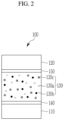
- FIG. 2 is a cross-sectional view showing another example of an infrared light sensor according to some example embodiments.
- an infrared light sensor 100 includes a first electrode 110 and a second electrode 120 facing each other, and an infrared photoelectric conversion layer 130 between the first electrode 110 and second electrode 120, like some example embodiments, including the example embodiments shown in FIG. 1 .
- the first electrode 110, the second electrode 120, and the infrared photoelectric conversion layer 130 are the same as described above.
- the infrared light sensor 100 further includes auxiliary layers 140 and 150 between the first electrode 110 and the infrared photoelectric conversion layer 130 and/or between the second electrode 120 and the infrared photoelectric conversion layer 130.
- the auxiliary layers 140 and 150 may be a charge auxiliary layer that may control transport rates of hole and/or electron separated from the infrared photoelectric conversion layer 130, an optical auxiliary layer that may control the absorption of incident light, or a combination thereof.
- the auxiliary layer 140 may be a hole injection layer (HIL) for facilitating hole injection to the anode, a hole transport layer (HTL) for facilitating hole transport to the anode, and/or an electron blocking layer (EBL) for preventing electron transport to the anode
- the auxiliary layer 150 may be an electron injection layer (EIL) for facilitating electron injection to the cathode, an electron transport layer (ETL) for facilitating electron transport to the cathode, and/or a hole blocking layer (HBL) for preventing hole transport to the cathode.
- HIL hole injection layer
- HTL hole transport layer
- EBL electron blocking layer
- the auxiliary layer 140 may be a hole transport layer and/or an electron blocking layer, and may include a fourth material having a wide energy band gap.
- the energy band gap of the fourth material may be wider (e.g., greater) than the energy band gaps of the first material 130a and the second material 130b included in the infrared photoelectric conversion layer 130.
- the energy band gap of the fourth material may be wider than the energy band gap of the first material 130a, by greater than or equal to about 1.0 eV, and within the above range, greater than or equal to about 1.0 eV, and within the above range, for example, greater than or equal to about 1.2 eV, greater than or equal to about 1.5 eV, or greater than or equal to about 1.7 eV, for example about 1.0 eV to about 5.0 eV, about 1.2 eV to about 5.0 eV, about 1.5 eV to about 5.0 eV, about 1.7 eV to about 5.0 eV, about 1.0 eV to about 4.5 eV, about 1.2 eV to about 4.5 eV, about 1.5 eV to about 4.5 eV, about 1.7 eV
- the energy band gap of the fourth material may be wider than the energy band gap of the second material 130b, by greater than or equal to about 0.5 eV, and within the above range, greater than or equal to about 0.7 eV, greater than or equal to about 0.9 eV, or greater than or equal to about 1.1 eV, for example, about 0.5 eV to about 3.0 eV, about 0.7 eV to about 3.0 eV, about 0.9 eV to about 3.0 eV, about 1.1 eV to about 3.0 eV, about 0.5 eV to about 2.5 eV, about 0.7 eV to about 2.5 eV, about 0.9 eV to about 2.5 eV, about 1.1 eV to about 2.5 eV, about 0.5 eV to about 2.0 eV, about 0.7 eV to about 2.0 eV, about 0.9 eV to about 2.0 eV, or about 1.1 eV to about 2.0 eV.
- the energy band gap of the fourth material may be, for example, greater than or equal to about 2.8 eV, and within the above range, about 2.8 eV to about 4.0 eV, about 2.8 eV to about 3.8 eV, or about 2.8 eV to about 3.5 eV.
- the HOMO energy level of the fourth material may be between a work function of the first electrode 110 and the HOMO energy level of the first material 130a of the infrared photoelectric conversion layer 130, for example, the work function of the first electrode 110, the HOMO energy level of the fourth material, and the HOMO energy level of the first material 130a of the infrared photoelectric conversion layer 130 may be a stepwise-type.
- the HOMO energy level of the fourth material may be about 4.8 eV to about 5.4 eV and within the above range, about 4.9 eV to about 5.4 eV or about 5.0 eV to about 5.4 eV.
- the auxiliary layer 140 includes a fourth material having these electrical properties and thus may effectively transport or extract holes from the infrared photoelectric conversion layer 130 to the first electrode 110 and simultaneously, effectively block a reverse flow of electrons from the first electrode 110 to the infrared photoelectric conversion layer 130, when a reverse bias is applied thereto.
- the fourth material may be the same as or different from the third material 130c described above.
- the auxiliary layer 140 may be a an electron injection layer (EIL) for facilitating electron injection, an electron transport layer (ETL) for facilitating electron transport, and/or a hole blocking layer (HBL) for preventing hole transport
- the auxiliary layer 150 may be a hole injection layer (HIL) for facilitating hole injection, a hole transport layer (HTL) for facilitating hole transport, and/or an electron blocking layer (EBL) for preventing electron transport.
- auxiliary layers 140 and/or 150 may include one of a first material 130a, a second material 130b, or a third material 130c.
- the auxiliary layer 140 may include a third material 130c.
- the auxiliary layer 150 may include the second material 130b.
- the auxiliary layer 140 and/or the auxiliary layer 150 may include the first material 130a.
- the fourth material may be represented by one of Chemical Formulae C-1 to C-9 as presented further below.
- auxiliary layers 140 and/or 150 may be omitted.
- FIG. 3 is a cross-sectional view showing an example of a sensor according to some example embodiments.
- the sensor 300 includes a semiconductor substrate 40, an insulation layer 80, and an infrared light sensor 100.
- the semiconductor substrate 40 may be a silicon substrate and is integrated with a transmission transistor (not shown) and a charge storage 55.
- the charge storage 55 may be integrated in each pixel.
- the charge storage 55 is electrically connected to the infrared light sensor 100 and information of the charge storage 55 may be transmitted by the transmission transistor.
- a metal wire (not shown) and a pad (not shown) are formed on the semiconductor substrate 40.
- the metal wire and pad may be made of a metal having low resistivity, for example, aluminum (Al), copper (Cu), silver (Ag), or alloys thereof, but is not limited thereto. However, it is not limited to the structure and the metal wire and pads may be disposed under the semiconductor substrate 40.
- the insulation layer 80 is formed on the metal wire and the pad.
- the insulation layer 80 may be made of an inorganic insulating material such as a silicon oxide and/or a silicon nitride, or a low dielectric constant (low K) material such as SiC, SiCOH, SiCO, and SiOF.
- the insulation layer 80 has a trench 85 exposing the charge storage 55.
- the trench 85 may be filled with fillers.
- the aforementioned infrared light sensor 100 is formed on the insulation layer 80.
- the infrared light sensor 100 includes the first electrode 110, the second electrode 120, and the infrared photoelectric conversion layer 130, as described above, and may further optionally include a charge auxiliary layer (not shown).
- the first electrode 110, the second electrode 120, and the infrared photoelectric conversion layer 130 are as described above.
- the second electrode 120 may be an incident electrode through which light is incident. Light of the infrared wavelength spectrum among the light incident through the second electrode 120 may be effectively absorbed by the infrared photoelectric conversion layer 130 and then photo-electrically converted. As described above, the dark current may be effectively suppressed under a reverse bias voltage, thereby exhibiting good photoelectric conversion characteristics by a combination of the first material 130a, the second material 130b, and the third material 130c of the infrared photoelectric conversion layer 130.
- the sensor 300 includes the infrared light sensor 100 of FIG. 1 , but is not limited thereto.
- the sensor 300 may include the infrared light sensor 100 of FIG. 2 .
- Focusing lens may be further formed on the infrared light sensor 100.
- the focusing lens may control a direction of incident light and gather the light in one region.
- the focusing lens may have a shape of, for example, a cylinder or a hemisphere, but is not limited thereto.
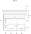
- FIG. 4 is a cross-sectional view showing an example of a sensor according to some example embodiments.
- the sensor according to some example embodiments, including the example embodiments shown in FIG. 4 may include a plurality of sensors having different functions. At least one of a plurality of sensors having different functions may be a biometric sensor.
- the biometric sensor may be for example an iris sensor, a depth sensor, a fingerprint sensor, or a blood vessel distribution sensor, but is not limited thereto.
- one of a plurality of sensors having different functions may be an iris sensor and the other may be a depth sensor.
- a plurality of sensors may include a first infrared light sensor configured to sense infrared light having a first wavelength ( ⁇ 1 ) within an infrared wavelength spectrum and a second infrared light sensor configured to sense infrared light having a second wavelength ( ⁇ 2 ) within an infrared wavelength spectrum.
- the first wavelength ( ⁇ 1 ) and the second wavelength ( ⁇ 2 ) may differ from each other within a wavelength spectrum of for example greater than about 700 nm and less than or equal to about 3000 nm.
- a difference between the first wavelength ( ⁇ 1 ) and the second wavelength ( ⁇ 2 ) may be greater than or equal to about 30 nm, greater than or equal to about 50 nm, greater than or equal to about 70 nm, greater than or equal to about 80 nm, or greater than or equal to about 90 nm.
- one of the first wavelength ( ⁇ 1 ) or the second wavelength ( ⁇ 2 ) may be within a wavelength spectrum of about 750 nm to about 1100 nm and the other of the first wavelength ( ⁇ 1 ) and the second wavelength ( ⁇ 2 ) may be within a wavelength spectrum of about 800 nm to about 1500 nm.
- the sensor 400 includes an optical filter 250; an upper infrared light sensor 100; an insulation layer 80; and a semiconductor substrate 40 in which a lower infrared light sensor 180 is integrated.
- the upper infrared light sensor 100 and the lower infrared light sensor 180 are stacked.
- the optical filter 250 may be disposed at the front side of the sensor 400, selectively transmitting infrared light including the first wavelength ( ⁇ 1 ) and infrared light including the second wavelength ( ⁇ 2 ), and blocking and/or absorbing other light.
- other light may also include light from ultraviolet (UV) and visible regions.
- the upper infrared light sensor 100 may be the same as the infrared light sensor 100 of some example embodiments, including the example embodiments shown in any of FIGS. 1-3 , and a detailed description thereof is omitted.
- FIG. 4 an example including the infrared light sensor 100 of FIG. 1 is illustrated, but is not limited thereto.
- the infrared light sensor 100 of FIG. 2 may be also included.
- the lower infrared light sensor 180 may be integrated in the semiconductor substrate 40 and may be a photodiode.
- the semiconductor substrate 40 may be for example a silicon substrate, in which a lower infrared light sensor 180, a charge storage 55, and a transmission transistor (not shown) are integrated.
- the light that is flowed into the lower infrared light sensor 180 may be light passing through the optical filter 250 and the upper infrared light sensor 100, and may be infrared light in a particular (or, alternatively, predetermined) region including a second wavelength ( ⁇ 2 ).
- the infrared light of a particular (or, alternatively, predetermined) region including the first wavelength ( ⁇ 1 ) may be all substantially absorbed in the infrared photoelectric conversion layer 130 of the upper infrared light sensor 100 and not reach the lower infrared light sensor 180.
- a separate filter for wavelength selectivity of light flowing in the lower infrared light sensor 180 is not needed.
- a filter between the upper infrared light sensor 100 and the lower infrared light sensor 180 may be additionally equipped.
- the sensor according to some example embodiments may not only include two infrared light sensors performing separate functions and thus function as a composite sensor but also maintain a size by stacking the two sensors performing the separate functions in each pixel and greatly improve sensitivity by doubling the number of the pixel.
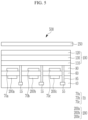
- FIG. 5 is a cross-sectional view showing an example of a sensor according to some example embodiments.
- the senor 500 includes an infrared light sensor 100, a visible light sensor 200, and an optical filter 250.
- the infrared light sensor 100 includes a first electrode 110, a second electrode 120, and an infrared photoelectric conversion layer 130 disposed between the first electrode 110 and the second electrode 120, as described above. Specific details thereof are the same as described above.
- the visible light sensor 200 is a sensor configured to sense light in the visible wavelength spectrum and may be a photodiode integrated in the semiconductor substrate 40.
- the visible light sensor 200 may be integrated in the semiconductor substrate 40 and may include a blue sensor 200a configured to sense light in a blue wavelength spectrum, a green sensor 200b configured to sense light in a green wavelength spectrum, and a red sensor 200c configured to sense light in a red wavelength spectrum. As shown in FIG.
- each of the blue sensor 200a, the green sensor 200b, and the red sensor 200c may be a photodiode that is integrated in the semiconductor substrate 40, such that the blue sensor 200a, the green sensor 200b, and the red sensor 200c are located within a volume space defined by outer surfaces of the semiconductor substrate 40 and may be partially or completely enclosed within an interior of the semiconductor substrate 40.
- the blue sensor 200a may be integrated in the blue pixel
- the green sensor 200b may be integrated in the green pixel
- the red sensor 200c may be integrated in the red pixel.
- the blue sensor 200a, the green sensor 200b, and the red sensor 200c are for example shown to be disposed at the same depth from the surface of the semiconductor substrate 40, but are not limited thereto, and may be disposed at different depths.
- the semiconductor substrate 40 may be for example a silicon substrate, and is integrated with a visible light sensor 200, a charge storage 55, and a transmission transistor (not shown).
- the visible light sensor 200 may sense light in a visible wavelength range passing through the optical filter 250, the infrared light sensor 100, and the color filter layer 70, and the sensed information may be transmitted by the transmission transistor.
- the charge storage 55 is electrically connected to the infrared light sensor 100.
- a metal wire (not shown) and a pad (not shown) are formed on the semiconductor substrate 40.
- the metal wire and pad may be made of a metal having low resistivity, for example, aluminum (Al), copper (Cu), silver (Ag), or alloys thereof, but is not limited thereto.
- Al aluminum
- Cu copper
- Ag silver
- the lower insulation layer 60 is formed on the semiconductor substrate 40.
- the lower insulation layer 60 may be made of an inorganic insulating material such as a silicon oxide and/or a silicon nitride, or a low dielectric constant (low K) material such as SiC, SiCOH, SiCO, and SiOF.
- the color filter layer 70 is formed on the lower insulation layer 60.
- the color filter layer 70 may include a blue filter 70a configured to selectively transmit light in the blue wavelength spectrum, a green filter 70b configured to selectively transmit light in a green wavelength spectrum, and a red filter 70c configured to selectively transmit light in the red wavelength spectrum.
- the blue filter 70a, the green filter 70b, and the red filter 70c are each overlapped with the blue sensor 200a, the green sensor 200b, and the red sensor 200c in the depth direction (e.g., the z direction).
- the blue filter 70a may selectively transmit light in a blue wavelength spectrum
- the green filter 70b may selectively transmit light in a green wavelength spectrum
- the red filter 70c may selectively transmit light in the red wavelength spectrum.
- the transmitted light of the blue wavelength spectrum may flow into the blue sensor 200a, the transmitted light of a green wavelength spectrum may flow into the green sensor 200b, and the transmitted light of the red wavelength spectrum may flow into the red sensor 200c.
- the present inventive concepts are not limited thereto, but at least one of the blue filter 70a, the green filter 70b, or the red filter 70c may be replaced with a yellow filter, a cyan filter, or a magenta filter.
- the color filter layer 70 is disposed between the infrared light sensor 100 and the visible light sensor 200 but not limited thereto and may be disposed on the infrared light sensor 100.
- the upper insulation layer 80 and color filter layer 70 may be between the infrared light sensor 100 and the optical filter 250.
- An upper insulation layer 80 (also referred to herein as an insulation layer 80) is formed on the color filter layer 70.
- the upper insulation layer 80 may be for example a planarization layer.
- the lower insulation layer 60 and the upper insulation layer 80 may have a trench 85 exposing the charge storage 55.
- the trench 85 may be filled with fillers. At least one of the lower insulation layer 60 or the upper insulation layer 80 may be omitted.
- the optical filter 250 is disposed on the visible light sensor 200 and the infrared light sensor 100 and specifically, on the whole surfaces of the visible light sensor 200 and the infrared light sensor 100.
- the optical filter 250 may selectively transmit light of a wavelength sensed in the visible light sensor 200 and light of a wavelength sensed in the infrared light sensor 100 but reflect or absorb and thus block light of the other wavelengths.
- Focusing lens may be further formed on the upper or lower surface of the optical filter 250.
- the focusing lens may control a direction of incident light and gather the light in one region.
- the focusing lens may have a shape of, for example, a cylinder or a hemisphere, but is not limited thereto.
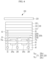
- FIG. 6 is a cross-sectional view showing an example of a sensor according to some example embodiments.
- the sensor 600 includes an infrared light sensor 100, a visible light sensor 200, and an optical filter 250, like some example embodiments, including the example embodiments shown in any of FIGS. 4-5 .
- the infrared light sensor 100 includes a first electrode 110, a second electrode 120, and an infrared photoelectric conversion layer 130 between the first electrode 110 and the second electrode 120, and specific details thereof are the same as described above.
- the visible light sensor 200 may be a combination of a photodiode integrated in the semiconductor substrate 40 and a photoelectric conversion device on the semiconductor substrate 40.
- a blue sensor 200a, a red sensor 200c, charge storages 55 and 240, and a transmission transistor are integrated.
- the blue sensor 200a and the red sensor 200c are photodiodes and disposed apart from each other in a horizontal direction of the semiconductor substrate 40.
- the blue sensor 200a is integrated in a blue pixel
- the red sensor 200c is integrated in a red pixel.
- the blue sensor 200a and the red sensor 200c are for example shown to be disposed at the same depth from the surface of the semiconductor substrate 40, but are not limited thereto and may be disposed at different depths.
- the color filter layer 70 includes a blue filter 70a overlapped with the blue sensor 200a and a red filter 70c overlapped with the red sensor 200c.
- An intermediate insulation layer 65 is formed on the color filter layer 70.
- the lower insulation layer 60 and the intermediate insulation layer 65 may have trenches 85 and 87 exposing the charge storages 55 and 240.
- the trenches 85 and 87 may be filled with fillers.
- At least one of the lower insulation layer 60 or the intermediate insulation layer 65 may be omitted.
- the green sensor 200b is formed on the intermediate insulation layer 65.
- the green sensor 200b may be a photoelectric conversion device and disposed on the whole surface.
- the green sensor 200b includes a lower electrode 210b and an upper electrode 220b facing each other and a green photoelectric conversion layer 230b between disposed between the lower electrode 210b and the upper electrode 220b.
- Either one of the lower electrode 210b or the upper electrode 220b is an anode, while the other one is a cathode.
- Both of the lower electrode 210b and the upper electrode 220b may be light-transmitting electrodes.
- the light-transmitting electrode may be for example made of a transparent conductor such as indium tin oxide (ITO), indium zinc oxide (IZO) or may be a metal thin film formed with a thin thickness of several nanometers to several tens of nanometer thickness or a single layer or multiple layers of metal thin film formed with a thin thickness of several nanometers to tens of nanometer thickness and doped with metal oxide.
- ITO indium tin oxide
- IZO indium zinc oxide
- metal thin film formed with a thin thickness of several nanometers to several tens of nanometer thickness or a single layer or multiple layers of metal thin film formed with a thin thickness of several nanometers to tens of nanometer thickness and doped with metal oxide.
- the green photoelectric conversion layer 230b may selectively absorb light in a green wavelength spectrum and allow light from wavelength spectrums other than the green wavelength spectrum, that is, the blue wavelength spectrum and the red wavelength spectrum, to pass through.
- the green photoelectric conversion layer 230b may be formed on the whole surface of the sensor 600. As a result, the green photoelectric conversion layer 230b may be configured to selectively absorb light in a green wavelength spectrum from the whole surface of the sensor 600 and increase light absorption areas, thus having high absorption efficiency.
- the green photoelectric conversion layer 230b may be configured to selectively absorb light of a green wavelength spectrum, forms excitons, and separates the excitons into holes and electrons, and as the separated holes move towards the anode which is one of the lower electrode 210b or the upper electrode 220b, while the separated electrons move toward the cathode which is the other one of the lower electrode 210b or the upper electrode 220b, a photoelectric conversion effect may be obtained.
- the separated electrons and/or holes may be gathered in charge storages 240.
- auxiliary layer may be further included between the lower electrode 210b and the green photoelectric conversion layer 230b and/or between the upper electrode 220b and the green photoelectric conversion layer 230b.
- the auxiliary layer may be a charge auxiliary layer, a light absorbing auxiliary layer, or a combination thereof, but is not limited thereto.
- the blue sensor 200a and the red sensor 200c are photodiodes and the green sensor 200b is a photoelectric conversion device is described, but is not limited thereto.
- the blue sensor 200a and the green sensor 200b may be photodiodes and the red sensor 200c may be a photoelectric conversion device or the green sensor 200b and the red sensor 200c may be photodiodes and the blue sensor 200a may be a photoelectric conversion device.
- two of the blue sensor 200a, the green sensor 200b, or the red sensor 200c may be integrated in the semiconductor substrate 40, and another of the blue sensor 200a, the green sensor 200b, or the red sensor 200c may be a visible light photoelectric conversion device on the semiconductor substrate 40 and stacked with the infrared light sensor 100 in a depth direction that is perpendicular to an in-plane direction of the infrared light sensor 100 (e.g., both the x and y directions) and/or is perpendicular to an upper surface of the semiconductor substrate 40 (e.g., the z direction).
- an upper insulation layer 80 is formed, and on the upper insulation layer 80, the infrared light sensor 100 and the optical filter 250 are disposed.
- the infrared light sensor 100 and the optical filter 250 are the same as described above.
- the color filter layer 70 and intermediate insulation layer 65 are between a photoelectric conversion device of the visible light sensor 200 (e.g., the green sensor 200b) and photodiodes of the visible light sensor 200 (e.g., the blue and red sensors 200a and 200c).
- a photoelectric conversion device of the visible light sensor 200 e.g., the green sensor 200b
- photodiodes of the visible light sensor 200 e.g., the blue and red sensors 200a and 200c.
- example embodiments are not limited thereto.
- the photoelectric conversion device of the visible light sensor 200 may be between the color filter layer 70 and photodiodes of the visible light sensor 200 (e.g., the blue and red sensors 200a and 200c) where the color filters of the color filter layer 70 are each configured to selectively transmit a mixture of the wavelength spectra absorbed by the photoelectric conversion device and a photodiode overlapped by the color filter.
- sensors 200a-200c may be configured to sense separate ones of red-green-blue (RGB) colors
- color filters 70a, 70c may be configured to selectively transmit separate ones of cyan-magenta-yellow CMY colors.
- the blue filter 70a which overlaps the blue sensor 200a in the depth direction
- the red filter 70c which overlaps the red sensor 200c in the depth direction
- the color filter layer 70 alone or together with the intermediate insulation layer 65, may be between the infrared light sensor 100 and the photoelectric conversion device (e.g., green sensor 200b) in the depth direction (e.g., in place of the insulation layer 80).
- the color filter layer 70, alone or together with the intermediate insulation layer 65 may be between the infrared light sensor 100 and the optical filter 250 in the depth direction.
- the sensor 600 is a composite sensor equipped with the infrared light sensor 100 and the visible light sensor 200 stacked on each other, and the visible light sensor 200 also has a structure of stacking the photodiode and the photoelectric conversion device and thus may further reduce an area of the sensor and thus down-sized the sensor.
- FIG. 7 is a cross-sectional view showing an example of a sensor according to some example embodiments.
- the senor 700 includes an infrared light sensor 100, a visible light sensor 200, and an optical filter 250, like some example embodiments, including the example embodiments shown in any of FIGS. 4-6 .
- the infrared light sensor 100 includes a first electrode 110, a second electrode 120, and an infrared photoelectric conversion layer 130 disposed between the first electrode 110 and the second electrode 120, and specific details thereof are the same as described above.
- the visible light sensor 200 includes a blue sensor 200a and a red sensor 200c integrated in a semiconductor substrate 40 and a green sensor 200b disposed on the semiconductor substrate 40.
- the blue sensor 200a and red sensor 200c may be photodiodes and the green sensor 200b may be a photoelectric conversion device.
- the green sensor 200b includes a lower electrode 210b, a green photoelectric conversion layer 230b, and an upper electrode 220b.
- the blue sensor 200a and the red sensor 200c integrated in the semiconductor substrate 40 in a vertical direction are stacked.
- the blue sensor 200a and the red sensor 200c may selectively absorb and sense light of each wavelength spectrum depending on a stacking depth.
- the red sensor 200c absorbing red light of a long wavelength spectrum and the blue sensor 200a absorbing blue light of a short wavelength spectrum are disposed deep from the surface of the semiconductor substrate 40.
- the color filter layer 70 may be omitted by separating absorption wavelengths depending on a stacking depth.
- the blue sensor 200a and the red sensor 200c are photodiodes and the green sensor 200b is a photoelectric conversion device is described, but is not limited thereto.
- the blue sensor 200a and the green sensor 200b may be photodiodes and the red sensor 200c may be a photoelectric conversion device or the green sensor 200b and the red sensor 200c may be photodiodes and the blue sensor 200a may be a photoelectric conversion device.
- the sensor 700 is a composite sensor equipped with the infrared light sensor 100 and the visible light sensor 200 stacked each other, and herein, since the visible light sensor 200 also may be equipped with the photodiode and the photoelectric conversion device stacked each other, and the photodiode also has a stacking structure, an area of the sensor may be further reduced, and accordingly, the sensor may be down-sized.
- the sensor 700 according to some example embodiments may not include a separate color filter layer and thus simplify a structure and a process.
- FIG. 8 is a cross-sectional view showing an example of a sensor according to some example embodiments.
- the senor 800 includes an infrared light sensor 100, a visible light sensor 200, and an optical filter 250, like some example embodiments, including the example embodiments shown in any of FIGS. 4-7 .
- the infrared light sensor 100 includes a first electrode 110, a second electrode 120, and an infrared photoelectric conversion layer 130 between the first electrode 110 and the second electrode 120, and specific details thereof are the same as described above.
- the visible light sensor 200 includes a blue sensor 200a, a green sensor 200b, and a red sensor 200c integrated in a semiconductor substrate 40.
- the blue sensor 200a, the green sensor 200b, and the red sensor 200c are stacked in a vertical direction in the semiconductor substrate 40.
- the blue sensor 200a, the green sensor 200b, and the red sensor 200c may separate an absorption wavelength according to a stacking depth, and thus the color filter layer 70 may be omitted.
- An insulation layer 80 is formed between the semiconductor substrate 40 and the infrared light sensor 100 and the insulation layer 80 has a trench 85.
- the semiconductor substrate 40 includes a charge storage 55 that is connected to the infrared light sensor 100.
- FIG. 9 is a perspective view showing an example of a sensor according to some example embodiments
- FIG. 10 is a cross-sectional view showing an example of the sensor shown in FIG. 9 .
- the sensor 900 includes a semiconductor substrate 40; an infrared light sensor 100; a visible light sensor 200; an insulation layer 80; and an optical filter 250.
- the visible light sensor 200 includes a blue sensor 200a, a green sensor 200b, and a red sensor 200c.
- the infrared light sensor 100, the blue sensor 200a, the green sensor 200b, and the red sensor 200c may be stacked in a horizontal direction on the semiconductor substrate 40, and may be each connected, via respective trenches 85, to the charge storages 55, 240a, 240b, and 240c integrated in the semiconductor substrate 40.
- the infrared light sensor 100, the blue sensor 200a, the green sensor 200b, and the red sensor 200c are each photoelectric conversion device.
- the infrared light sensor 100 includes a first electrode 110, a second electrode 120, and an infrared photoelectric conversion layer 130 disposed between the first electrode 110 and the second electrode 120, and specific details thereof are the same as described above.
- the blue sensor 200a includes a lower electrode 210a, a blue photoelectric conversion layer 230a, and an upper electrode 220a.
- the green sensor 200b includes a lower electrode 210b, a green photoelectric conversion layer 230b, and an upper electrode 220b.
- the red sensor 200c includes a lower electrode 210c, a red photoelectric conversion layer 230c, and an upper electrode 220c.
- the blue photoelectric conversion layer 230a may selectively absorb light in a blue wavelength spectrum to perform photoelectric conversion
- the green photoelectric conversion layer 230b may selectively absorb light in a green wavelength spectrum to perform photoelectric conversion
- the red photoelectric conversion layer 230c may selectively absorb light in a red wavelength spectrum to perform photoelectric conversion.
- FIG. 11 is a perspective view showing an example of a sensor according to some example embodiments
- FIG. 12 is a cross-sectional view showing an example of the sensor shown in FIG. 11 .
- a sensor 1000 includes a semiconductor substrate 40; an infrared light sensor 100; a visible light sensor 200; and an optical filter 250.
- the visible light sensor 200 includes a blue sensor 200a, a green sensor 200b, and a red sensor 200c.
- the infrared light sensor 100, the blue sensor 200a, the green sensor 200b, and the red sensor 200c may be stacked in a vertical direction on the semiconductor substrate 40, and may be each connected, via respective trenches 85, to charge storages 55, 240a, 240b, and 240c integrated in the semiconductor substrate 40.
- the infrared light sensor 100 includes a first electrode 110, a second electrode 120, and an infrared photoelectric conversion layer 130 disposed between the first electrode 110 and the second electrode 120, and specific details thereof are the same as described above.
- the blue sensor 200a includes a lower electrode 210a, a blue photoelectric conversion layer 230a, and an upper electrode 220a.
- the green sensor 200b includes a lower electrode 210b, a green photoelectric conversion layer 230b, and an upper electrode 220b.
- the red sensor 200c includes a lower electrode 210c, a red photoelectric conversion layer 230c, and an upper electrode 220c.
- Insulation layers 80a, 80b, 80c, and 80d are respectively disposed between the semiconductor substrate 40 and the blue sensor 200a, between the blue sensor 200a and the green sensor 200b, between the green sensor 200b and the red sensor 200c, and between the red sensor 200c and the infrared light sensor 100.
- each of the blue sensor 200a, the green sensor 200b, and the red sensor 200c may be a visible light photoelectric conversion device that is stacked with the infrared light sensor 100 in a depth direction that is perpendicular to an in-plane direction of the infrared light sensor 100 (e.g., both the x and y directions) and/or is perpendicular to an upper surface of the semiconductor substrate 40 (e.g., the z direction).
- a sensor may include an infrared light sensor 100, a visible light sensor 200, and a semiconductor substrate 40.
- the infrared light sensor 100 may be arranged in parallel with the visible light sensor 200 along an in-plane direction (e.g., the xy plane) in which both the infrared light sensor 100 and the visible light sensor 200 extend.
- the infrared light sensor 100 may be stacked with the visible light sensor 200 along a depth direction of the semiconductor substrate 40.
- the depth direction may be understood to be perpendicular to an upper surface of the semiconductor substrate 40.
- the depth direction may be understood to be perpendicular to the in-plane direction(s) in which the infrared light sensor 100 extends, for example the x and y directions.
- the aforementioned sensor may be applied to (e.g., included in) various electronic devices, for example mobile phones, digital cameras, computers, tablet PC, biometric devices, and/or automotive electronic components, but the present inventive concepts are not limited thereto.
- FIG. 13 is a schematic diagram of an electronic device according to some example embodiments.
- an electronic device 1300 includes a processor 1320, a memory 1330, a sensor 1340, and a display device 1350 (e.g., an OLED display screen device) electrically connected through a bus 1310.
- the sensor 1340 may be any of the aforementioned various sensors 100, 300, 400, 500, 600, 700, 800, 900, and/or 1000.
- the processor 1320 may perform a memory program and thus at least one function.
- the processor 1320 may additionally perform a memory program and thus display an image on the display device 1350.
- the processor 1320 may generate an output.
- One or more of the processor 1320, memory 1330, sensor 1340, or display device 1350 may be included in, include, and/or implement one or more instances of processing circuitry such as hardware including logic circuits, a hardware/software combination such as a processor executing software; or a combination thereof.
- said one or more instances of processing circuitry may include, but are not limited to, a central processing unit (CPU), an application processor (AP), an arithmetic logic unit (ALU), a graphic processing unit (GPU), a digital signal processor, a microcomputer, a field programmable gate array (FPGA), a System-on-Chip (SoC) a programmable logic unit, a microprocessor, or an application-specific integrated circuit (ASIC), etc.
- CPU central processing unit
- AP application processor
- ALU arithmetic logic unit
- GPU graphic processing unit
- FPGA field programmable gate array
- SoC System-on-Chip
- any of the memories, memory units, or the like as described herein may include a non-transitory computer readable storage device, for example a solid state drive (SSD), storing a program of instructions, and the one or more instances of processing circuitry may be configured to execute the program of instructions to implement the functionality of some or all of any of the electronic device 1300, processor 1320, memory 1330, sensor 1340, display device 1350, or the like according to any of the example embodiments as described herein.
- SSD solid state drive
- a compound represented by Chemical Formula C-1 (HOMO: 5.08 eV, LUMO: 1.98 eV) is deposited on an Ag reflector (Work function: 4.7 eV) to form a 20 nm-thick lower auxiliary layer.
- Sn-naphthalocyanine dichloride represented by Chemical Formula A first material, p-type semiconductor, ⁇ max,A : 870 nm, HOMO: 5.16 eV, LUMO: 3.96 eV
- C60 represented by Chemical Formula B (second material, n-type semiconductor, ⁇ max,A : 450 nm, HOMO: 6.0 eV, LUMO: 4.3 eV)
- a compound represented by Chemical Formula C-1 (third material, HOMO: 5.08 eV, LUMO: 1.98 eV) are co-deposited in a thickness ratio (a volume ratio) of 40:150:20 to form a 210 nm-thick infrared
- C60 is deposited to form a 15 nm-thick upper auxiliary layer, and silver (Ag) is deposited on the upper auxiliary layer to form a 30 nm-thick upper electrode, manufacturing an infrared sensor.
- An infrared sensor is manufactured according to the same method as Example 1-1 except that the first material, the second material, and the third material are co-deposited in a thickness ratio (volume ratio) of 40:150:40 to form a 230 nm-thick infrared photoelectric conversion layer.
- An infrared sensor is manufactured according to the same method as Example 1-1 except that the first material, the second material, and the third material are co-deposited in a thickness ratio (volume ratio) of 40:150:60 to form a 250 nm-thick infrared photoelectric conversion layer.
- An infrared sensor is manufactured according to the same method as Example 1-1 except that a compound represented by Chemical Formula C-2 (HOMO: 5.14 eV, LUMO: 2.04 eV) instead of the compound represented by Chemical Formula C-1 is used as the third material, and the first material, the second material, and the third material are co-deposited in a thickness ratio (a volume ratio) of 40:150:40 to form a 230 nm-thick infrared photoelectric conversion layer.
- a compound represented by Chemical Formula C-2 HOMO: 5.14 eV, LUMO: 2.04 eV
- An infrared sensor is manufactured according to the same method as Example 1-1 except that a compound represented by Chemical Formula C-3 (HOMO: 5.29 eV, LUMO: 2.29 eV) instead of the compound represented by Chemical Formula C-1 is used as the third material, and the first material, the second material, and the third material are co-deposited in a thickness ratio (a volume ratio) of 45:140:35 to form a 220 nm-thick infrared photoelectric conversion layer.
- a compound represented by Chemical Formula C-3 HOMO: 5.29 eV, LUMO: 2.29 eV
- An infrared sensor is manufactured according to the same method as Example 1-1 except that a compound represented by Chemical Formula C-4 (HOMO: 4.96 eV, LUMO: 1.80 eV) instead of the compound represented by Chemical Formula C-1 is used as the third material, and the first material, the second material, and the third material are co-deposited in a thickness ratio (a volume ratio) of 45:140:30 to form a 215 nm-thick infrared photoelectric conversion layer.
- a compound represented by Chemical Formula C-4 HOMO: 4.96 eV, LUMO: 1.80 eV
- An infrared sensor is manufactured according to the same method as Example 1-1 except that a compound represented by Chemical Formula C-5 (HOMO: 5.25 eV, LUMO: 2.01 eV) instead of the compound represented by Chemical Formula C-1 is used as the third material, and the first material, the second material, and the third material are co-deposited in a thickness ratio (a volume ratio) of 45:140:30 to form a 215 nm-thick infrared photoelectric conversion layer.
- a compound represented by Chemical Formula C-5 HOMO: 5.25 eV, LUMO: 2.01 eV
- An infrared sensor is manufactured according to the same method as Example 1-1 except that a compound represented by Chemical Formula C-6 (HOMO: 5.73 eV, LUMO: 2.54 eV) instead of the compound represented by Chemical Formula C-1 is used as the third material, and the first material, the second material, and the third material are co-deposited in a thickness ratio (a volume ratio) of 45:140:30 to form a 215 nm-thick infrared photoelectric conversion layer.
- a compound represented by Chemical Formula C-6 HOMO: 5.73 eV, LUMO: 2.54 eV
- An infrared sensor is manufactured according to the same method as Example 1-1 except that a compound represented by Chemical Formula C-7 (HOMO: 5.41 eV, LUMO: 2.49 eV) instead of the compound represented by Chemical Formula C-1 is used as the third material, and the first material, the second material, and the third material are co-deposited in a thickness ratio (a volume ratio) of 45:140:30 to form a 215 nm-thick infrared photoelectric conversion layer.
- a compound represented by Chemical Formula C-7 HOMO: 5.41 eV, LUMO: 2.49 eV
- An infrared sensor is manufactured according to the same method as Example 1-1 except that a compound represented by Chemical Formula C-8 (HOMO: 5.36 eV, LUMO: 2.32 eV) instead of the compound represented by Chemical Formula C-1 is used as the third material, and the first material, the second material, and the third material are co-deposited in a thickness ratio (a volume ratio) of 45:140:30 to form a 215 nm-thick infrared photoelectric conversion layer.
- a compound represented by Chemical Formula C-8 HOMO: 5.36 eV, LUMO: 2.32 eV
- An infrared sensor is manufactured according to the same method as Example 1-1 except that a compound represented by Chemical Formula C-9 (HOMO: 6.00 eV, LUMO: 2.67 eV) instead of the compound represented by Chemical Formula C-1 is used as the third material, and the first material, the second material, and the third material are co-deposited in a thickness ratio (a volume ratio) of 45:140:30 to form a 215 nm-thick infrared photoelectric conversion layer.
- a compound represented by Chemical Formula C-9 HOMO: 6.00 eV, LUMO: 2.67 eV
- An infrared sensor is manufactured according to the same method as Example 1-1 except that the first material and the second material are co-deposited in a thickness ratio (volume ratio) of 40:150 without the third material to form a 190 nm-thick infrared photoelectric conversion layer.
- the absorption spectra and EQE spectra of the infrared sensors which may be the absorption spectra and EQE spectra of the respective infrared photoelectric conversion layers contained therein, are respectively evaluated by using an UV-Visible spectrophotometer and an Incident Photon to Current Conversion Efficiency (IPCE) equipment. The results are shown in Table 1.
- Example 1 Table 1 ⁇ max, A (nm) ⁇ max, EQE (nm) Example 1-1 1150 1150 Example 1-2 1250 1250 Example 1-3 1270 1270 Example 2 1230 1230 Example 3 1200 1200 Example 4 1195 1195 Example 5 1195 1195 Example 6 1185 1185 Example 7 1200 1200 Example 8 1200 1200 Example 9 1190 1190 Comparative Example 1 1110 1110 * ⁇ max, A : maximum absorption wavelength * ⁇ max, EQE : maximum EQE wavelength
- the absorption spectra (maximum absorption wavelength) and EQE spectra (maximum EQE wavelength) of the infrared sensors according to Examples are shifted toward a long wavelength spectrum, compared with the infrared sensors according to Comparative Example.
- the absorption spectrum (maximum absorption wavelength) and the EQE spectrum (maximum EQE wavelength) of the infrared sensors of the Examples are further shifted toward the longer wavelength spectrum in relation to that of the Comparative Example 1.
- the number of charge trap sites is converted from Capacitance-Voltage characteristics measured by using an Impedance analyzer.
- the dark current is evaluated by using dark current density, which is obtained by measuring the dark current with a current-voltage evaluation equipment (Keithley K4200 parameter analyzer, Keithley Instrument, LLC) and dividing it with a unit pixel area (0.04 cm 2 ).
- the dark current density is evaluated from a current flowing when - 3 V reverse bias is applied. The results are shown in Table 2.
- Example 1-1 31 1.2 ⁇ 10 5
- Example 1-2 5.6 5.2 ⁇ 10 4
- Example 1-3 6.2 4.4 ⁇ 10 4
- Example 2 47 1.5 ⁇ 10 5
- Example 3 49 7.7 ⁇ 10 4
- Example 5 - 9.3 ⁇ 10 4
- Example 6 8.3 ⁇ 10 4
- Example 7 - 1.2 ⁇ 10 5
- Example 8 - 1.2 ⁇ 10 5 Comparative Example 1 466 3.3 ⁇ 10 5
- the infrared sensors according to the Examples exhibit a smaller number of charge trap sites and lower dark current density, compared with the infrared sensors according to Comparative Example 1.
- the third material is included in a larger amount in the infrared photoelectric conversion layer, the number of the charge trap sites and the dark current density become much smaller.
Landscapes
- Physics & Mathematics (AREA)
- Chemical & Material Sciences (AREA)
- Electromagnetism (AREA)
- Spectroscopy & Molecular Physics (AREA)
- Engineering & Computer Science (AREA)
- Materials Engineering (AREA)
- Light Receiving Elements (AREA)
- Inorganic Chemistry (AREA)
Claims (14)
- Sensor (100, 300, 400, 500, 600, 700, 800, 900, 1000, 1340), umfassendeine erste Elektrode (110) und eine zweite Elektrode (120); undeine infrarote fotoelektrische Umwandlungsschicht (130) zwischen der ersten Elektrode und der zweiten Elektrode, wobei die infrarote fotoelektrische Umwandlungsschicht dazu konfiguriert ist, Licht in mindestens einem Abschnitt eines infraroten Wellenlängenspektrums zu absorbieren und das absorbierte Licht in ein elektrisches Signal umzuwandeln,wobei die infrarote fotoelektrische Umwandlungsschicht beinhaltetein erstes Material (130a) mit einer maximalen Absorptionswellenlänge in dem infraroten Wellenlängenspektrum,ein zweites Material (130b), das einen pn-Übergang mit dem ersten Material bildet, undein drittes Material (130c), das ein organisches Material ist und eine Energiebandlücke aufweist, die um größer oder gleich 1,0 eV größer ist als eine Energiebandlücke des ersten Materials,wobei das erste Material, das zweite Material und dritte Material voneinander verschieden sind,wobei jedes des ersten Materials, des zweiten Materials und des dritten Materials ein nichtpolymeres Material ist, unddadurch gekennzeichnet, dassdie infrarote fotoelektrische Umwandlungsschicht ein Gemisch aus dem ersten Material, dem zweiten Material und dem dritten Material umfasst.
- Sensor nach Anspruch 1, wobei eine Differenz zwischen einem HOMO-Energieniveau des ersten Materials und einem HOMO-Energieniveau des dritten Materials weniger als 1,0 eV ist; und/oderwobei eine Differenz zwischen einem HOMO-Energieniveau des zweiten Materials und einem HOMO-Energieniveau des ersten Materials größer oder gleich 0,5 eV ist; und/oderwobei die Energiebandlücke des ersten Materials 0,5 eV bis 1,8 eV ist und die Energiebandlücke des dritten Materials 2,8 eV bis 4,0 eV ist; und/oderwobei die Energiebandlücke des dritten Materials größer ist als eine Energiebandlücke des zweiten Materials.
- Sensor nach Ansprüchen 1 oder 2, wobei das erste Material in der infraroten fotoelektrischen Umwandlungsschicht in einer kleineren Volumenmenge beinhaltet ist als das zweite Material, bevorzugt, wobei ein Zusammensetzungsverhältnis des ersten Materials zu dem zweiten Material in der infraroten fotoelektrischen Umwandlungsschicht 0,10 bis 0,90, bevorzugt 0,10 bis 0,50 ist; und/oder
wobei jedes des ersten Materials und des dritten Materials in der infraroten fotoelektrischen Umwandlungsschicht in einer kleineren Volumenmenge beinhaltet ist als das zweite Material. - Sensor nach einem der Ansprüche 1-3, wobei das dritte Material in der infraroten fotoelektrischen Umwandlungsschicht in einer Menge von 1 Volumen-% bis 40 Volumen-%, bevorzugt 7 Volumen-% bis 25 Volumen-%, basierend auf einem Gesamtvolumen der infraroten fotoelektrischen Umwandlungsschicht, beinhaltet ist; und/oder
wobei eine maximale Absorptionswellenlänge der infraroten fotoelektrischen Umwandlungsschicht länger ist als die maximale Absorptionswellenlänge des ersten Materials. - Sensor nach einem der Ansprüche 1-4, wobei das dritte Material dargestellt ist von der chemischen Formel 1:
 L1 und L2 unabhängig eine Einfachbindung, eine substituierte oder unsubstituierte C1- bis C30-Alkylengruppe, eine substituierte oder unsubstituierte C6- bis C30-Arylengruppe oder eine Kombination davon sind,Ar1 bis Ar4 unabhängig eine substituierte oder unsubstituierte C6- bis C30-Arylgruppe sind,Ar1 und Ar2 unabhängig vorliegen oder miteinander kombiniert sind, um einen Ring zu bilden,Ar3 und Ar4 unabhängig vorliegen oder miteinander kombiniert sind, um einen Ring zu bilden,R1 bis R4 unabhängig Wasserstoff, Deuterium, eine substituierte oder unsubstituierte C1-bis C30-Alkylgruppe, eine substituierte oder unsubstituierte C1- bis C30-Alkoxygruppe, eine substituierte oder unsubstituierte C6- bis C30-Arylgruppe, eine substituierte oder unsubstituierte C3- bis C30-Heteroarylgruppe, eine substituierte oder unsubstituierte Amingruppe, eine substituierte oder unsubstituierte C6- bis C30-Arylamingruppe, Halogen, Cyanogruppe oder eine Kombination davon sind,R1 bis R4 unabhängig vorliegen oder zwei von R1 bis R4, die nebeneinander sind, kombiniert sind, um einen Ring zu bilden, undm eine ganze Zahl von 0 bis 2 ist;bevorzugt, wobei das dritte Material dargestellt ist von einer der chemischen Formeln 1-1 bis 1-8: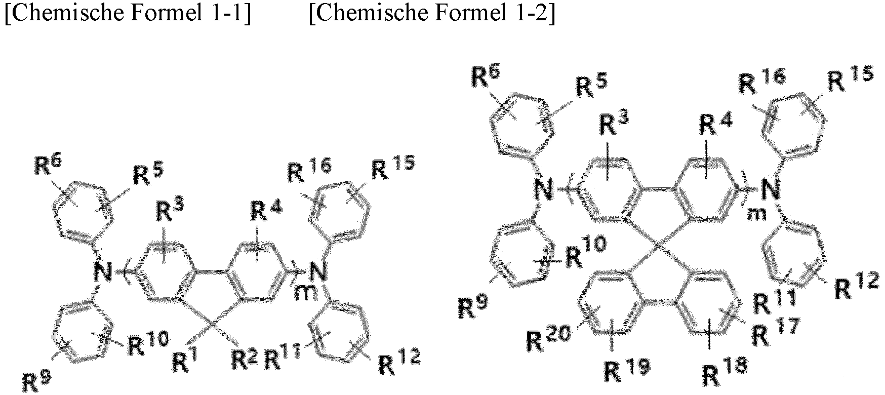


 wobei, in den chemischen Formeln 1-1 bis 1-8,R1 bis R22 unabhängig Wasserstoff, Deuterium, eine substituierte oder unsubstituierte C1-bis C30-Alkylgruppe, eine substituierte oder unsubstituierte C1- bis C30-Alkoxygruppe, eine substituierte oder unsubstituierte C6- bis C30-Arylgruppe, eine substituierte oder unsubstituierte C3- bis C30-Heteroarylgruppe, eine substituierte oder unsubstituierte Amingruppe, eine substituierte oder unsubstituierte C6- bis C30-Arylamingruppe, Halogen, Cyanogruppe oder eine Kombination davon sind,R1 bis R22 unabhängig vorliegen oder zwei von R1 bis R22, die nebeneinander sind, kombiniert sind, um einen Ring zu bilden, undm 1 oder 2 ist.
 - Sensor nach einem der Ansprüche 1-5, wobei die infrarote fotoelektrische Umwandlungsschicht ein ternäres System aus dem ersten Material, dem zweiten Material und dem dritten Material ist.
- Sensor nach einem der Ansprüche 1-6, wobei der Sensor eine maximale externe Quanteneffizienzwellenlänge aufweist, die in einem Bereich von 800 nm bis 1500 nm ist; und/oder
wobei der Sensor ferner umfasst:eine erste Hilfsschicht zwischen der ersten Elektrode und der infraroten fotoelektrischen Umwandlungsschicht,die erste Hilfsschicht ein viertes Material umfasst, wobei das vierte Material ein gleiches Material wie das dritte Material ist oder sich von dem dritten Material unterscheidet,die Energiebandlücke des vierten Materials um größer oder gleich 1,0 eV größer ist als die Energiebandlücke des ersten Materials, undein HOMO-Energieniveau des vierten Materials zwischen einer Arbeitsfunktion der ersten Elektrode und einem HOMO-Energieniveau des ersten Materials ist. - Sensor (100, 300, 400, 500, 600, 700, 800, 900, 1000, 1340) nach einem der Ansprüche 1-7, wobei das dritte Material (130c) von der chemischen Formel 1 dargestellt ist, undwobei eine maximale Absorptionswellenlänge der infraroten fotoelektrischen Umwandlungsschicht länger ist als die maximale Absorptionswellenlänge des ersten Materials:
 wobei, in der chemischen Formel 1,L1 und L2 unabhängig eine Einfachbindung, eine substituierte oder unsubstituierte C1- bis C30-Alkylengruppe, eine substituierte oder unsubstituierte C6- bis C30-Arylengruppe oder eine Kombination davon sind,Ar1 bis Ar4 unabhängig eine substituierte oder unsubstituierte C6- bis C30-Arylgruppe sind,Ar1 und Ar2 unabhängig vorliegen oder miteinander kombiniert sind, um einen Ring zu bilden,Ar3 und Ar4 unabhängig vorliegen oder miteinander kombiniert sind, um einen Ring zu bilden,R1 bis R4 unabhängig Wasserstoff, Deuterium, eine substituierte oder unsubstituierte C1-bis C30-Alkylgruppe, eine substituierte oder unsubstituierte C1- bis C30-Alkoxygruppe, eine substituierte oder unsubstituierte C6- bis C30-Arylgruppe, eine substituierte oder unsubstituierte C3- bis C30-Heteroarylgruppe, eine substituierte oder unsubstituierte Amingruppe, eine substituierte oder unsubstituierte C6- bis C30-Arylamingruppe, Halogen, Cyanogruppe oder eine Kombination davon sind,R1 bis R4 unabhängig vorliegen oder zwei von R1 bis R4, die nebeneinander sind, kombiniert sind, um einen Ring zu bilden, undm eine ganze Zahl von 0 bis 2 ist.
 - Sensor nach Anspruch 8, wobei die maximale Absorptionswellenlänge der infraroten fotoelektrischen Umwandlungsschicht um größer oder gleich 30 nm länger ist als die maximale Absorptionswellenlänge des ersten Materials.
- Sensor nach Ansprüchen 8 oder 9, wobei das dritte Material in der infraroten fotoelektrischen Umwandlungsschicht in einer Menge von 1 Volumen-% bis 40 Volumen-%, bevorzugt 7 Volumen-% bis 25 Volumen-%, basierend auf einem Gesamtvolumen der infraroten fotoelektrischen Umwandlungsschicht, beinhaltet ist.
- Sensor nach einem der Ansprüche 8-10, wobeidie maximale Absorptionswellenlänge des ersten Materials zu 750 nm bis 1200 nm gehört, unddie maximale Absorptionswellenlänge der infraroten fotoelektrischen Umwandlungsschicht zu 1000 bis 1500 nm gehört.
- Sensor nach einem der Ansprüche 8-11, wobei das dritte Material dargestellt ist von einer der chemischen Formeln 1-1 bis 1-8:

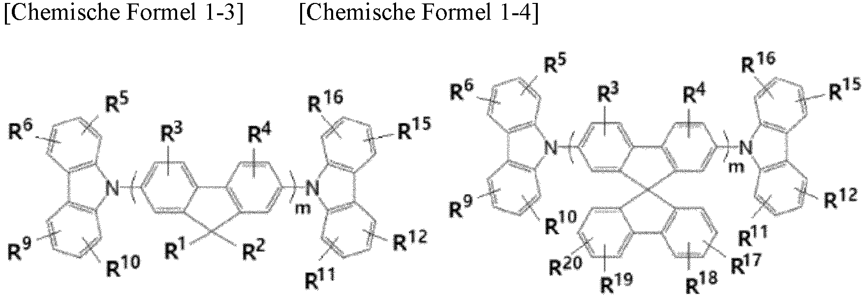


 wobei, in den chemischen Formeln 1-1 bis 1-8,R1 bis R22 unabhängig Wasserstoff, Deuterium, eine substituierte oder unsubstituierte C1-bis C30-Alkylgruppe, eine substituierte oder unsubstituierte C1- bis C30-Alkoxygruppe, eine substituierte oder unsubstituierte C6- bis C30-Arylgruppe, eine substituierte oder unsubstituierte C3- bis C30-Heteroarylgruppe, eine substituierte oder unsubstituierte Amingruppe, eine substituierte oder unsubstituierte C6- bis C30-Arylamingruppe, ein Halogen, eine Cyanogruppe oder eine Kombination davon sind,R1 bis R22 unabhängig vorliegen oder zwei von R1 bis R22, die nebeneinander sind, kombiniert sind, um einen Ring zu bilden, undm 1 oder 2 ist.
 - Sensor nach einem der Ansprüche 8-12, wobei das erste Material einen Metall-Phthalocyanin-Komplex oder einen Metall-Naphthalocyanin-Komplex umfasst.
- Elektronische Vorrichtung (1300), umfassend den Sensor nach einem der Ansprüche 1-13.
Applications Claiming Priority (2)
| Application Number | Priority Date | Filing Date | Title |
|---|---|---|---|
| KR20200141347 | 2020-10-28 | ||
| KR1020210141666A KR20220056803A (ko) | 2020-10-28 | 2021-10-22 | 센서 및 전자 장치 |
Publications (2)
| Publication Number | Publication Date |
|---|---|
| EP3993052A1 EP3993052A1 (de) | 2022-05-04 |
| EP3993052B1 true EP3993052B1 (de) | 2025-03-26 |
Family
ID=78676267
Family Applications (1)
| Application Number | Title | Priority Date | Filing Date |
|---|---|---|---|
| EP21204420.0A Active EP3993052B1 (de) | 2020-10-28 | 2021-10-25 | Sensor und elektronische vorrichtung |
Country Status (3)
| Country | Link |
|---|---|
| US (1) | US12178056B2 (de) |
| EP (1) | EP3993052B1 (de) |
| CN (1) | CN114497377A (de) |
Families Citing this family (3)
| Publication number | Priority date | Publication date | Assignee | Title |
|---|---|---|---|---|
| US12490574B2 (en) * | 2021-02-08 | 2025-12-02 | Uif (University Industry Foundation), Yonsei University | Skin-conformable biosignal monitoring sensor by applying organic-inorganic hybrid photo transistor and manufacturing method thereof |
| KR102926962B1 (ko) * | 2021-06-29 | 2026-02-11 | 삼성전자주식회사 | 열 또는 적외선 감지용 센서 및 이를 포함하는 전자장치 |
| JP7798303B1 (ja) * | 2024-07-17 | 2026-01-14 | Nttイノベーティブデバイス株式会社 | 受光デバイス |
Family Cites Families (18)
| Publication number | Priority date | Publication date | Assignee | Title |
|---|---|---|---|---|
| US20070181179A1 (en) * | 2005-12-21 | 2007-08-09 | Konarka Technologies, Inc. | Tandem photovoltaic cells |
| CN102017214B (zh) | 2008-03-19 | 2014-03-19 | 密执安州立大学董事会 | 用于红外探测的有机薄膜 |
| AU2010324764A1 (en) | 2009-11-24 | 2012-06-14 | University Of Florida Research Foundation, Inc. | Method and apparatus for sensing infrared radiation |
| KR101703311B1 (ko) | 2010-03-08 | 2017-02-13 | 삼성전자주식회사 | 적외선 센서, 이를 포함하는 터치패널 및 입체용 컬러 이미지센서 |
| JP6025243B2 (ja) | 2012-05-10 | 2016-11-16 | 富士フイルム株式会社 | 光電変換素子及びそれを用いた撮像素子 |
| US10651409B2 (en) * | 2012-07-20 | 2020-05-12 | Nutech Ventures | Narrowband nanocomposite photodetector |
| JP6010514B2 (ja) | 2013-09-27 | 2016-10-19 | 富士フイルム株式会社 | 光電変換素子および撮像素子 |
| JP7141826B2 (ja) | 2015-03-17 | 2022-09-26 | 日産化学株式会社 | 光センサ素子の正孔捕集層形成用組成物および光センサ素子 |
| CN107331776B (zh) | 2017-07-18 | 2019-12-06 | 电子科技大学 | 一种基于电荷转移复合物的新型有机近红外光电探测器 |
| US10998514B2 (en) | 2017-12-01 | 2021-05-04 | Samsung Electronics Co., Ltd. | Photoelectric devices and image sensors and electronic devices |
| KR102491496B1 (ko) * | 2018-01-05 | 2023-01-20 | 삼성전자주식회사 | 광전 소자, 이미지 센서 및 전자 장치 |
| KR102590315B1 (ko) | 2018-05-28 | 2023-10-16 | 삼성전자주식회사 | 유기 광전 소자 및 이를 포함하는 적층형 이미지 센서 |
| JP7235465B2 (ja) | 2018-10-01 | 2023-03-08 | 住友化学株式会社 | 光電変換素子及びその製造方法 |
| EP3901194A4 (de) | 2018-12-20 | 2022-03-02 | Mitsubishi Chemical Corporation | Organische lichtdiode und infrarot-cmos-sensor |
| US20200212329A1 (en) | 2018-12-27 | 2020-07-02 | Samsung Electronics Co., Ltd. | Photoelectric conversion film, photoelectric conversion device, and image sensor |
| JP2020107736A (ja) | 2018-12-27 | 2020-07-09 | 三星電子株式会社Samsung Electronics Co.,Ltd. | 光電変換膜、光電変換素子および撮像素子 |
| KR102819099B1 (ko) * | 2019-09-16 | 2025-06-10 | 삼성전자주식회사 | 근적외선 흡수재, 근적외선 흡수/차단 필름, 광전 소자, 유기 센서 및 전자 장치 |
| US11793007B2 (en) * | 2019-11-05 | 2023-10-17 | Samsung Electronics Co., Ltd. | Photoelectric conversion devices and sensors and electronic devices |
-
2021
- 2021-10-25 EP EP21204420.0A patent/EP3993052B1/de active Active
- 2021-10-25 US US17/509,451 patent/US12178056B2/en active Active
- 2021-10-28 CN CN202111261026.8A patent/CN114497377A/zh active Pending
Also Published As
| Publication number | Publication date |
|---|---|
| US12178056B2 (en) | 2024-12-24 |
| US20220131098A1 (en) | 2022-04-28 |
| EP3993052A1 (de) | 2022-05-04 |
| CN114497377A (zh) | 2022-05-13 |
Similar Documents
| Publication | Publication Date | Title |
|---|---|---|
| EP3509108B1 (de) | Photoelektrische vorrichtungen und bildsensoren und elektronische vorrichtungen | |
| US11849597B2 (en) | Sensors and electronic devices | |
| CN112500423B (zh) | 近红外吸收剂、近红外吸收/阻挡膜、光电器件、有机传感器和电子装置 | |
| EP3993052B1 (de) | Sensor und elektronische vorrichtung | |
| EP3696857A1 (de) | Photoelektrische dioden und organische sensoren und elektronische vorrichtungen | |
| US11437438B2 (en) | Photoelectric conversion devices and organic sensors and electronic devices | |
| US12178125B2 (en) | Photoelectric conversion device and sensor and electronic device | |
| US11929384B2 (en) | Image sensors and electronic devices | |
| EP3960738B1 (de) | Verbindung, film und ir-sensor sowie kombinationssensor und elektronische vorrichtung | |
| US11855236B2 (en) | Sensors and electronic devices | |
| US11591347B2 (en) | Compounds and films and photoelectric diodes and organic sensors and electronic devices | |
| US11631819B2 (en) | Photoelectric conversion device, organic sensor and electronic device | |
| EP3739642A1 (de) | Vorrichtungen zur photoelektrischen umwandlung und organische sensoren und elektronische vorrichtungen | |
| EP4174063A1 (de) | Verbindung, film, sensor und elektronische vorrichtung | |
| US11557741B2 (en) | Photoelectric conversion devices and organic sensors and electronic devices | |
| KR20220056803A (ko) | 센서 및 전자 장치 | |
| EP3660935A1 (de) | Photoelektrische umwandlungsvorrichtungen und organische sensoren und elektronische vorrichtungen |
Legal Events
| Date | Code | Title | Description |
|---|---|---|---|
| PUAI | Public reference made under article 153(3) epc to a published international application that has entered the european phase |
Free format text: ORIGINAL CODE: 0009012 |
|
| STAA | Information on the status of an ep patent application or granted ep patent |
Free format text: STATUS: THE APPLICATION HAS BEEN PUBLISHED |
|
| AK | Designated contracting states |
Kind code of ref document: A1 Designated state(s): AL AT BE BG CH CY CZ DE DK EE ES FI FR GB GR HR HU IE IS IT LI LT LU LV MC MK MT NL NO PL PT RO RS SE SI SK SM TR |
|
| STAA | Information on the status of an ep patent application or granted ep patent |
Free format text: STATUS: REQUEST FOR EXAMINATION WAS MADE |
|
| 17P | Request for examination filed |
Effective date: 20221031 |
|
| RBV | Designated contracting states (corrected) |
Designated state(s): AL AT BE BG CH CY CZ DE DK EE ES FI FR GB GR HR HU IE IS IT LI LT LU LV MC MK MT NL NO PL PT RO RS SE SI SK SM TR |
|
| P01 | Opt-out of the competence of the unified patent court (upc) registered |
Effective date: 20230519 |
|
| STAA | Information on the status of an ep patent application or granted ep patent |
Free format text: STATUS: EXAMINATION IS IN PROGRESS |
|
| 17Q | First examination report despatched |
Effective date: 20230912 |
|
| REG | Reference to a national code |
Ref country code: DE Free format text: PREVIOUS MAIN CLASS: H01L0027300000 Ipc: H10K0030300000 Ref country code: DE Ref legal event code: R079 Ref document number: 602021028060 Country of ref document: DE Free format text: PREVIOUS MAIN CLASS: H01L0027300000 Ipc: H10K0030300000 |
|
| RIC1 | Information provided on ipc code assigned before grant |
Ipc: H10K 30/20 20230101ALN20240911BHEP Ipc: H10K 30/10 20230101ALN20240911BHEP Ipc: H10K 85/30 20230101ALN20240911BHEP Ipc: H10K 85/20 20230101ALN20240911BHEP Ipc: H10K 85/60 20230101ALI20240911BHEP Ipc: H10K 39/32 20230101ALI20240911BHEP Ipc: H10K 30/30 20230101AFI20240911BHEP |
|
| GRAP | Despatch of communication of intention to grant a patent |
Free format text: ORIGINAL CODE: EPIDOSNIGR1 |
|
| STAA | Information on the status of an ep patent application or granted ep patent |
Free format text: STATUS: GRANT OF PATENT IS INTENDED |
|
| RIC1 | Information provided on ipc code assigned before grant |
Ipc: H10K 30/20 20230101ALN20240913BHEP Ipc: H10K 30/10 20230101ALN20240913BHEP Ipc: H10K 85/30 20230101ALN20240913BHEP Ipc: H10K 85/20 20230101ALN20240913BHEP Ipc: H10K 85/60 20230101ALI20240913BHEP Ipc: H10K 39/32 20230101ALI20240913BHEP Ipc: H10K 30/30 20230101AFI20240913BHEP |
|
| INTG | Intention to grant announced |
Effective date: 20241023 |
|
| GRAS | Grant fee paid |
Free format text: ORIGINAL CODE: EPIDOSNIGR3 |
|
| GRAA | (expected) grant |
Free format text: ORIGINAL CODE: 0009210 |
|
| STAA | Information on the status of an ep patent application or granted ep patent |
Free format text: STATUS: THE PATENT HAS BEEN GRANTED |
|
| AK | Designated contracting states |
Kind code of ref document: B1 Designated state(s): AL AT BE BG CH CY CZ DE DK EE ES FI FR GB GR HR HU IE IS IT LI LT LU LV MC MK MT NL NO PL PT RO RS SE SI SK SM TR |
|
| REG | Reference to a national code |
Ref country code: GB Ref legal event code: FG4D |
|
| REG | Reference to a national code |
Ref country code: CH Ref legal event code: EP |
|
| REG | Reference to a national code |
Ref country code: DE Ref legal event code: R096 Ref document number: 602021028060 Country of ref document: DE |
|
| REG | Reference to a national code |
Ref country code: IE Ref legal event code: FG4D |
|
| PG25 | Lapsed in a contracting state [announced via postgrant information from national office to epo] |
Ref country code: RS Free format text: LAPSE BECAUSE OF FAILURE TO SUBMIT A TRANSLATION OF THE DESCRIPTION OR TO PAY THE FEE WITHIN THE PRESCRIBED TIME-LIMIT Effective date: 20250626 |
|
| PG25 | Lapsed in a contracting state [announced via postgrant information from national office to epo] |
Ref country code: FI Free format text: LAPSE BECAUSE OF FAILURE TO SUBMIT A TRANSLATION OF THE DESCRIPTION OR TO PAY THE FEE WITHIN THE PRESCRIBED TIME-LIMIT Effective date: 20250326 |
|
| REG | Reference to a national code |
Ref country code: LT Ref legal event code: MG9D |
|
| PG25 | Lapsed in a contracting state [announced via postgrant information from national office to epo] |
Ref country code: NO Free format text: LAPSE BECAUSE OF FAILURE TO SUBMIT A TRANSLATION OF THE DESCRIPTION OR TO PAY THE FEE WITHIN THE PRESCRIBED TIME-LIMIT Effective date: 20250626 |
|
| PG25 | Lapsed in a contracting state [announced via postgrant information from national office to epo] |
Ref country code: HR Free format text: LAPSE BECAUSE OF FAILURE TO SUBMIT A TRANSLATION OF THE DESCRIPTION OR TO PAY THE FEE WITHIN THE PRESCRIBED TIME-LIMIT Effective date: 20250326 |
|
| PG25 | Lapsed in a contracting state [announced via postgrant information from national office to epo] |
Ref country code: LV Free format text: LAPSE BECAUSE OF FAILURE TO SUBMIT A TRANSLATION OF THE DESCRIPTION OR TO PAY THE FEE WITHIN THE PRESCRIBED TIME-LIMIT Effective date: 20250326 |
|
| PG25 | Lapsed in a contracting state [announced via postgrant information from national office to epo] |
Ref country code: GR Free format text: LAPSE BECAUSE OF FAILURE TO SUBMIT A TRANSLATION OF THE DESCRIPTION OR TO PAY THE FEE WITHIN THE PRESCRIBED TIME-LIMIT Effective date: 20250627 Ref country code: BG Free format text: LAPSE BECAUSE OF FAILURE TO SUBMIT A TRANSLATION OF THE DESCRIPTION OR TO PAY THE FEE WITHIN THE PRESCRIBED TIME-LIMIT Effective date: 20250326 |
|
| REG | Reference to a national code |
Ref country code: NL Ref legal event code: MP Effective date: 20250326 |
|
| PG25 | Lapsed in a contracting state [announced via postgrant information from national office to epo] |
Ref country code: NL Free format text: LAPSE BECAUSE OF FAILURE TO SUBMIT A TRANSLATION OF THE DESCRIPTION OR TO PAY THE FEE WITHIN THE PRESCRIBED TIME-LIMIT Effective date: 20250326 |
|
| PG25 | Lapsed in a contracting state [announced via postgrant information from national office to epo] |
Ref country code: SE Free format text: LAPSE BECAUSE OF FAILURE TO SUBMIT A TRANSLATION OF THE DESCRIPTION OR TO PAY THE FEE WITHIN THE PRESCRIBED TIME-LIMIT Effective date: 20250326 |
|
| REG | Reference to a national code |
Ref country code: AT Ref legal event code: MK05 Ref document number: 1780308 Country of ref document: AT Kind code of ref document: T Effective date: 20250326 |
|
| PG25 | Lapsed in a contracting state [announced via postgrant information from national office to epo] |
Ref country code: SM Free format text: LAPSE BECAUSE OF FAILURE TO SUBMIT A TRANSLATION OF THE DESCRIPTION OR TO PAY THE FEE WITHIN THE PRESCRIBED TIME-LIMIT Effective date: 20250326 |
|
| PG25 | Lapsed in a contracting state [announced via postgrant information from national office to epo] |
Ref country code: PT Free format text: LAPSE BECAUSE OF FAILURE TO SUBMIT A TRANSLATION OF THE DESCRIPTION OR TO PAY THE FEE WITHIN THE PRESCRIBED TIME-LIMIT Effective date: 20250728 Ref country code: ES Free format text: LAPSE BECAUSE OF FAILURE TO SUBMIT A TRANSLATION OF THE DESCRIPTION OR TO PAY THE FEE WITHIN THE PRESCRIBED TIME-LIMIT Effective date: 20250326 |
|
| PG25 | Lapsed in a contracting state [announced via postgrant information from national office to epo] |
Ref country code: IT Free format text: LAPSE BECAUSE OF FAILURE TO SUBMIT A TRANSLATION OF THE DESCRIPTION OR TO PAY THE FEE WITHIN THE PRESCRIBED TIME-LIMIT Effective date: 20250326 Ref country code: PL Free format text: LAPSE BECAUSE OF FAILURE TO SUBMIT A TRANSLATION OF THE DESCRIPTION OR TO PAY THE FEE WITHIN THE PRESCRIBED TIME-LIMIT Effective date: 20250326 |
|
| PGFP | Annual fee paid to national office [announced via postgrant information from national office to epo] |
Ref country code: GB Payment date: 20250911 Year of fee payment: 5 |
|
| PG25 | Lapsed in a contracting state [announced via postgrant information from national office to epo] |
Ref country code: AT Free format text: LAPSE BECAUSE OF FAILURE TO SUBMIT A TRANSLATION OF THE DESCRIPTION OR TO PAY THE FEE WITHIN THE PRESCRIBED TIME-LIMIT Effective date: 20250326 |
|
| PGFP | Annual fee paid to national office [announced via postgrant information from national office to epo] |
Ref country code: FR Payment date: 20250908 Year of fee payment: 5 |
|
| PG25 | Lapsed in a contracting state [announced via postgrant information from national office to epo] |
Ref country code: EE Free format text: LAPSE BECAUSE OF FAILURE TO SUBMIT A TRANSLATION OF THE DESCRIPTION OR TO PAY THE FEE WITHIN THE PRESCRIBED TIME-LIMIT Effective date: 20250326 |
|
| PG25 | Lapsed in a contracting state [announced via postgrant information from national office to epo] |
Ref country code: RO Free format text: LAPSE BECAUSE OF FAILURE TO SUBMIT A TRANSLATION OF THE DESCRIPTION OR TO PAY THE FEE WITHIN THE PRESCRIBED TIME-LIMIT Effective date: 20250326 |
|
| PG25 | Lapsed in a contracting state [announced via postgrant information from national office to epo] |
Ref country code: SK Free format text: LAPSE BECAUSE OF FAILURE TO SUBMIT A TRANSLATION OF THE DESCRIPTION OR TO PAY THE FEE WITHIN THE PRESCRIBED TIME-LIMIT Effective date: 20250326 |
|
| PG25 | Lapsed in a contracting state [announced via postgrant information from national office to epo] |
Ref country code: IS Free format text: LAPSE BECAUSE OF FAILURE TO SUBMIT A TRANSLATION OF THE DESCRIPTION OR TO PAY THE FEE WITHIN THE PRESCRIBED TIME-LIMIT Effective date: 20250726 |
|
| REG | Reference to a national code |
Ref country code: DE Ref legal event code: R097 Ref document number: 602021028060 Country of ref document: DE |
|
| PGFP | Annual fee paid to national office [announced via postgrant information from national office to epo] |
Ref country code: DE Payment date: 20250910 Year of fee payment: 5 |
|
| PG25 | Lapsed in a contracting state [announced via postgrant information from national office to epo] |
Ref country code: DK Free format text: LAPSE BECAUSE OF FAILURE TO SUBMIT A TRANSLATION OF THE DESCRIPTION OR TO PAY THE FEE WITHIN THE PRESCRIBED TIME-LIMIT Effective date: 20250326 |
|
| PG25 | Lapsed in a contracting state [announced via postgrant information from national office to epo] |
Ref country code: CZ Free format text: LAPSE BECAUSE OF FAILURE TO SUBMIT A TRANSLATION OF THE DESCRIPTION OR TO PAY THE FEE WITHIN THE PRESCRIBED TIME-LIMIT Effective date: 20250326 |
|
| PLBE | No opposition filed within time limit |
Free format text: ORIGINAL CODE: 0009261 |
|
| STAA | Information on the status of an ep patent application or granted ep patent |
Free format text: STATUS: NO OPPOSITION FILED WITHIN TIME LIMIT |
|
| REG | Reference to a national code |
Ref country code: CH Ref legal event code: L10 Free format text: ST27 STATUS EVENT CODE: U-0-0-L10-L00 (AS PROVIDED BY THE NATIONAL OFFICE) Effective date: 20260211 |
|
| 26N | No opposition filed |
Effective date: 20260105 |