EP3993171A1 - Connecteur enfichable aveugle, système de transfert de données et procédé d'affichage d'une capacité d'alimentation électrique - Google Patents
Connecteur enfichable aveugle, système de transfert de données et procédé d'affichage d'une capacité d'alimentation électrique Download PDFInfo
- Publication number
- EP3993171A1 EP3993171A1 EP21204972.0A EP21204972A EP3993171A1 EP 3993171 A1 EP3993171 A1 EP 3993171A1 EP 21204972 A EP21204972 A EP 21204972A EP 3993171 A1 EP3993171 A1 EP 3993171A1
- Authority
- EP
- European Patent Office
- Prior art keywords
- unit
- plug
- circuit board
- contacts
- data
- Prior art date
- Legal status (The legal status is an assumption and is not a legal conclusion. Google has not performed a legal analysis and makes no representation as to the accuracy of the status listed.)
- Pending
Links
Images




Classifications
-
- H—ELECTRICITY
- H01—ELECTRIC ELEMENTS
- H01R—ELECTRICALLY-CONDUCTIVE CONNECTIONS; STRUCTURAL ASSOCIATIONS OF A PLURALITY OF MUTUALLY-INSULATED ELECTRICAL CONNECTING ELEMENTS; COUPLING DEVICES; CURRENT COLLECTORS
- H01R24/00—Two-part coupling devices, or either of their cooperating parts, characterised by their overall structure
- H01R24/60—Contacts spaced along planar side wall transverse to longitudinal axis of engagement
- H01R24/62—Sliding engagements with one side only, e.g. modular jack coupling devices
- H01R24/64—Sliding engagements with one side only, e.g. modular jack coupling devices for high frequency, e.g. RJ 45
-
- H—ELECTRICITY
- H01—ELECTRIC ELEMENTS
- H01R—ELECTRICALLY-CONDUCTIVE CONNECTIONS; STRUCTURAL ASSOCIATIONS OF A PLURALITY OF MUTUALLY-INSULATED ELECTRICAL CONNECTING ELEMENTS; COUPLING DEVICES; CURRENT COLLECTORS
- H01R13/00—Details of coupling devices of the kinds covered by groups H01R12/70 or H01R24/00 - H01R33/00
- H01R13/66—Structural association with built-in electrical component
- H01R13/717—Structural association with built-in electrical component with built-in light source
- H01R13/7175—Light emitting diodes (LEDs)
-
- G—PHYSICS
- G01—MEASURING; TESTING
- G01R—MEASURING ELECTRIC VARIABLES; MEASURING MAGNETIC VARIABLES
- G01R1/00—Details of instruments or arrangements of the types included in groups G01R5/00 - G01R13/00 and G01R31/00
- G01R1/02—General constructional details
- G01R1/04—Housings; Supporting members; Arrangements of terminals
- G01R1/0408—Test fixtures or contact fields; Connectors or connecting adaptors; Test clips; Test sockets
- G01R1/0416—Connectors, terminals
-
- H—ELECTRICITY
- H01—ELECTRIC ELEMENTS
- H01R—ELECTRICALLY-CONDUCTIVE CONNECTIONS; STRUCTURAL ASSOCIATIONS OF A PLURALITY OF MUTUALLY-INSULATED ELECTRICAL CONNECTING ELEMENTS; COUPLING DEVICES; CURRENT COLLECTORS
- H01R12/00—Structural associations of a plurality of mutually-insulated electrical connecting elements, specially adapted for printed circuits, e.g. printed circuit boards [PCB], flat or ribbon cables, or like generally planar structures, e.g. terminal strips, terminal blocks; Coupling devices specially adapted for printed circuits, flat or ribbon cables, or like generally planar structures; Terminals specially adapted for contact with, or insertion into, printed circuits, flat or ribbon cables, or like generally planar structures
- H01R12/70—Coupling devices
- H01R12/7005—Guiding, mounting, polarizing or locking means; Extractors
- H01R12/7011—Locking or fixing a connector to a PCB
-
- H—ELECTRICITY
- H01—ELECTRIC ELEMENTS
- H01R—ELECTRICALLY-CONDUCTIVE CONNECTIONS; STRUCTURAL ASSOCIATIONS OF A PLURALITY OF MUTUALLY-INSULATED ELECTRICAL CONNECTING ELEMENTS; COUPLING DEVICES; CURRENT COLLECTORS
- H01R13/00—Details of coupling devices of the kinds covered by groups H01R12/70 or H01R24/00 - H01R33/00
- H01R13/44—Means for preventing access to live contacts
- H01R13/443—Dummy plugs
-
- H—ELECTRICITY
- H01—ELECTRIC ELEMENTS
- H01R—ELECTRICALLY-CONDUCTIVE CONNECTIONS; STRUCTURAL ASSOCIATIONS OF A PLURALITY OF MUTUALLY-INSULATED ELECTRICAL CONNECTING ELEMENTS; COUPLING DEVICES; CURRENT COLLECTORS
- H01R13/00—Details of coupling devices of the kinds covered by groups H01R12/70 or H01R24/00 - H01R33/00
- H01R13/46—Bases; Cases
- H01R13/52—Dustproof, splashproof, drip-proof, waterproof, or flameproof cases
- H01R13/5213—Covers
-
- H—ELECTRICITY
- H01—ELECTRIC ELEMENTS
- H01R—ELECTRICALLY-CONDUCTIVE CONNECTIONS; STRUCTURAL ASSOCIATIONS OF A PLURALITY OF MUTUALLY-INSULATED ELECTRICAL CONNECTING ELEMENTS; COUPLING DEVICES; CURRENT COLLECTORS
- H01R13/00—Details of coupling devices of the kinds covered by groups H01R12/70 or H01R24/00 - H01R33/00
- H01R13/66—Structural association with built-in electrical component
- H01R13/665—Structural association with built-in electrical component with built-in electronic circuit
-
- H—ELECTRICITY
- H05—ELECTRIC TECHNIQUES NOT OTHERWISE PROVIDED FOR
- H05K—PRINTED CIRCUITS; CASINGS OR CONSTRUCTIONAL DETAILS OF ELECTRIC APPARATUS; MANUFACTURE OF ASSEMBLAGES OF ELECTRICAL COMPONENTS
- H05K3/00—Apparatus or processes for manufacturing printed circuits
- H05K3/40—Forming printed elements for providing electric connections to or between printed circuits
- H05K3/403—Edge contacts; Windows or holes in the substrate having plural connections on the walls thereof
-
- H—ELECTRICITY
- H01—ELECTRIC ELEMENTS
- H01R—ELECTRICALLY-CONDUCTIVE CONNECTIONS; STRUCTURAL ASSOCIATIONS OF A PLURALITY OF MUTUALLY-INSULATED ELECTRICAL CONNECTING ELEMENTS; COUPLING DEVICES; CURRENT COLLECTORS
- H01R2107/00—Four or more poles
-
- H—ELECTRICITY
- H01—ELECTRIC ELEMENTS
- H01R—ELECTRICALLY-CONDUCTIVE CONNECTIONS; STRUCTURAL ASSOCIATIONS OF A PLURALITY OF MUTUALLY-INSULATED ELECTRICAL CONNECTING ELEMENTS; COUPLING DEVICES; CURRENT COLLECTORS
- H01R2201/00—Connectors or connections adapted for particular applications
- H01R2201/20—Connectors or connections adapted for particular applications for testing or measuring purposes
-
- H—ELECTRICITY
- H05—ELECTRIC TECHNIQUES NOT OTHERWISE PROVIDED FOR
- H05K—PRINTED CIRCUITS; CASINGS OR CONSTRUCTIONAL DETAILS OF ELECTRIC APPARATUS; MANUFACTURE OF ASSEMBLAGES OF ELECTRICAL COMPONENTS
- H05K1/00—Printed circuits
- H05K1/18—Printed circuits structurally associated with non-printed electric components
- H05K1/181—Printed circuits structurally associated with non-printed electric components associated with surface mounted components
-
- H—ELECTRICITY
- H05—ELECTRIC TECHNIQUES NOT OTHERWISE PROVIDED FOR
- H05K—PRINTED CIRCUITS; CASINGS OR CONSTRUCTIONAL DETAILS OF ELECTRIC APPARATUS; MANUFACTURE OF ASSEMBLAGES OF ELECTRICAL COMPONENTS
- H05K2201/00—Indexing scheme relating to printed circuits covered by H05K1/00
- H05K2201/09—Shape and layout
- H05K2201/09145—Edge details
- H05K2201/09181—Notches in edge pads
-
- H—ELECTRICITY
- H05—ELECTRIC TECHNIQUES NOT OTHERWISE PROVIDED FOR
- H05K—PRINTED CIRCUITS; CASINGS OR CONSTRUCTIONAL DETAILS OF ELECTRIC APPARATUS; MANUFACTURE OF ASSEMBLAGES OF ELECTRICAL COMPONENTS
- H05K2201/00—Indexing scheme relating to printed circuits covered by H05K1/00
- H05K2201/10—Details of components or other objects attached to or integrated in a printed circuit board
- H05K2201/10007—Types of components
- H05K2201/10106—Light emitting diode [LED]
Definitions
- the invention relates to a dummy plug according to the preamble of claim 1, a data transmission system according to claim 16 and a method for displaying a power supply capacity according to claim 17.
- a data transmission system in particular an RJ45 system, is already known from the prior art, which is intended to provide a Power over Ethernet (PoE) connection.
- a data connector unit of the data transmission system is already known, which can be connected to a counter data connector unit of the data transmission system, in particular an RJ45 socket, with the counter data connector unit defining a PoE connection for a PoE connection.
- a test plug of the data transmission system can be used to check whether an electrical voltage is present at the mating data plug unit and whether it is the PoE connection.
- the test plug can be connected to the mating data plug unit for checking the electrical voltage, with the test plug being separated from the mating data plug unit again after the check.
- a dummy plug in particular an RJ45 dummy plug, is also known from the prior art, which can be plugged into the mating data plug unit for dust protection.
- the object of the invention is in particular to provide a generic device with improved properties in terms of efficiency.
- the object is achieved according to the invention by the features of claims 1, 16 and 17, while advantageous refinements and developments of the invention can be found in the dependent claims.
- the invention is based on a dummy plug, in particular an RJ45 dummy plug, with at least one data plug unit, which is provided for a connection to a counter data plug unit, in particular an RJ45 socket.
- the data plug unit has an output unit which is intended to display a power supply capacity of the mating data plug unit.
- the output unit can be used to determine whether the mating data plug unit is a classic Ethernet connection or a Power over Ethernet (PoE) connection. Thus, the power supply capacity of Ethernet systems can be tested.
- the mating data plug unit in particular the electronics of the mating data plug unit, can be protected from dust and/or external influences by means of the dummy plug. Consequently, due to the multifunctionality of the dummy plug, additional devices, in particular test plugs and/or separate dust protection, can be dispensed with.
- the data transmission system can recognize the connected dummy plug and adapt and/or control and/or regulate activation of the dummy plug to the dummy plug.
- the data transmission system in particular the RJ45 system, could, for example, have at least one network, in particular a local area network (LAN), preferably an Ethernet network.
- the data transmission system is intended to provide at least one data connection, in particular Ethernet connection, for data transmission between at least one power sourcing equipment (PSE) of the data transmission system and a receiving unit of the data transmission system.
- the receiving unit could, for example, be a power device (PD) or also a dummy plug according to the invention, in particular an RJ45 dummy plug.
- the PSE could be a router and/or a hub and/or advantageously a switch.
- the data transmission system is preferably capable of providing a power supply for the receiving unit in addition to the data connection.
- PoE Power over Ethernet
- the PD is, for example, a static surveillance camera and/or a VoIP phone and/or an IP phone and/or a computer and/or a flat screen and/or an alarm system.
- the data transmission system preferably has the counterpart data plug unit, in particular an RJ45 socket, for a connection between the receiving unit and the PSE.
- the mating data plug unit comprises at least two mating contacts, preferably eight mating contacts.
- the mating contacts could, for example, consist at least partially and/or to a large extent of a metal, in particular copper or gold and/or another electrically conductive material and/or a composite material.
- the expression “for the most part” should be understood to mean, for example, at least 55%, advantageously at least 65%, preferably at least 75%, particularly preferably at least 85% and particularly advantageously at most 95% of a volume and/or mass fraction.
- the mating contacts each form pairs, in particular the mating contacts form four pairs.
- at least two of the pairs of mating contacts are provided for transmission of the data signal and/or the power supply.
- exactly two of the pairs of mating contacts could transmit the data signal and/or the power supply.
- a PoE connection via two of the pairs of mating contacts designates a PoE type 1 connection, in particular in accordance with the IEEE 802.3af standard.
- a PoE type 2 connection in particular according to the IEEE 802.3at standard, to be able to be established via two of the pairs of mating contacts.
- four of the mating contact pairs could carry the data signal and/or power.
- a PoE connection that runs over four of the pairs of mating contacts is a PoE type 3 connection or a PoE type 4 connection, in particular according to the IEEE 802.3bt (type 3) standard or according to the IEEE 802.3bt (type 4) Default.
- the data signal and the power supply could, for example, be transmittable via two different pairs of the pairs of mating contacts.
- the mating contact pair carrying the data signal could be identical to the mating contact pair carrying the power supply transmits.
- the data signal can be transmitted via four of the pairs of counter-contacts and that the power supply can be provided by two of these four pairs of counter-contacts.
- the power supply capacity of the mating data plug unit can preferably be measured and/or displayed, in particular on at least two of the pairs of mating contacts.
- the dummy plug indicates the power supply capacity of at least two of the pairs of mating contacts.
- the dummy plug could be designed to indicate a PoE type connection.
- the dummy plug could be used to indicate via which of the pairs of mating contacts the PoE connection, in particular the PoE type connection, runs.
- the data signal and/or the power supply could be transferrable between the counter data connector unit and the receiving unit.
- the dummy plug In a mounted state, the dummy plug is preferably connected to the counter data plug unit, so that in the operating state the dummy plug checks and displays the power supply capacity of the counter data plug unit for the PoE connection.
- the PSE checks and/or recognizes whether at least the PD or the dummy plug is connected to the counterpart data plug unit. If the PD is connected to the counterpart data connector unit, the PSE could enable and/or regulate the transmission of the data signal and the power supply, in particular a PoE voltage.
- the PSE could detect whether the dummy plug is connected to the mating data plug unit in the assembled state.
- the data transmission system could carry out at least one or more different tests to check whether a PoE connection can be established with the receiving unit, in particular whether a PD is connected to the counter data connector unit.
- the PSE simulates the PD.
- the PSE could detect the receiving unit by means of a detection signal.
- the detection signal contains at least one interrogation pulse, in particular several individual interrogation pulses.
- the PSE could at least send the request pulse to the receiving unit.
- the interrogation pulse is standardized.
- the query pulse could, for example, have a test voltage of at least 2.8 V, advantageously at least 10 V and particularly preferably at most 30 V, and for example a query duration of at least 0.1 s, advantageously at least 0.2 s and particularly preferably at most 0.5 s.
- the interrogation pulse has a short-circuit current of, for example, at most 2 mA, preferably at most 3 mA and particularly preferably at most 5 mA. It would be conceivable for the PSE to repeat the test, in particular the interrogation pulse, for example at a rhythm of in particular 5 s, preferably 3 s and particularly preferably 2 s, until the PSE recognizes a connected PD.
- the PSE could recognize the connected PD if at least one load of in particular at least 19 kOhm, preferably at least 23 kOhm and advantageously at most 26.5 kOhm is detectable.
- a capacitance of the connected PD is limited to, for example, at least 100 nF, preferably at least 120 nF, and particularly preferably to 150 nF.
- the PSE could reject the detected receiving unit as the connected PD if the load is less than 15 kOhm or preferably exceeds at least 33 kOhm.
- the PSE In the installed state and in at least the operating state, the PSE checks the receiving unit connected to the counterpart data connector unit. In particular, the PSE recognizes the dummy plug. In the mounted state and in the operating state, the dummy plug is preferably connected to the counter data plug unit via the data plug unit and is able to indicate the current capacity supply of the counter data plug unit, in particular the PSE, by means of the output unit.
- the output unit is in at least one output state for an optical and/or acoustic output, in particular a display, for an operator.
- the output unit could visually and/or acoustically indicate to the operator, for example by means of a light signal, and/or acoustically, for example by means of a signal tone, the current power supply capacity of the mating data connector unit.
- the output unit could, in the output state, send and/or transmit a signal, for example a radio signal, to an external device, for example a mobile terminal device, in particular a smartphone.
- the dummy plug preferably provides dust protection for the mating data plug unit in the mounted state and in particular at least in the operating state.
- Provided is intended to mean specifically programmed, designed, and/or equipped. Including that an object is intended for a specific function be understood that the object fulfills and/or executes this specific function in at least one application and/or operating state.
- At least one electrical parameter of the output unit is below or above a limit value of the electrical parameter for detection as a power device (PD).
- PD power device
- efficiency can be further increased since the PSE only establishes a PoE connection with a PD and supplies the PD with a data signal and a PoE voltage when the PSE detects the PD. Since the number of mating data plug units via which the PoE connection can be established is limited in the case of power-limited PSEs, the connected dummy plug can be recognized by means of the interrogation pulse. As a result, the PSE can use the data signal and the PoE voltage to control only that mating data connector unit which is connected to the PD, and efficiency with regard to control of the receiving unit can thus be further optimized.
- the electrical parameter is the aforementioned load.
- the PSE could recognize the dummy plug when the electrical parameter, in particular the load, is advantageously less than 15 kOhm. In at least the assembled state and in at least the operational state, the PSE could only provide power for the dummy plug.
- the PSE preferably operates the dummy plug, in particular the output unit, with the detection signal, in particular the test voltage of the interrogation pulse.
- the output unit may include electronic paper (e-paper, e-paper).
- the output unit advantageously has at least one light source, in particular an LED.
- the light source can be connected directly to the mating data plug unit, in particular by means of a direct electrical contact, so that the output unit is free of at least one series resistor.
- the illuminant could be a green or blue LED, for example.
- the LED is orange-red or red. That emitted by the lighting means could be particularly preferred Light has a wavelength of in particular at least 600 nm, preferably at least 625 nm and advantageously at most 640 nm.
- the illuminant is a low-current LED.
- the LED designed as a low-current LED could light up in at least the operating state when the power supply is in particular at least 5 mA, advantageously at least 2 mA and particularly preferably at least 1 mA. It would be conceivable for the LED to display the query pulse directly. Here, the LED could flash in at least the output state.
- the LED in the display state, could emit light for at least 0.5 s, for example, and be switched off for at least 1.5 s, for example.
- the LED could be permanently lit in an output state, in particular the LED is permanently lit if the PSE simulates the PD in at least the operating state. In a further output state of the output unit, the LED could be switched off completely.
- the data plug unit has at least one printed circuit board which has contacts for making contact with mating contacts of the mating data plug unit. This enables energy-efficient and precise electrical contacting between the data plug unit, in particular the LED, and the mating data plug unit.
- the printed circuit board has at least a top and a bottom.
- the contacts could be located on the top or bottom of the circuit board.
- the contacts preferably extend over a side of the printed circuit board that faces the mating data plug unit, in particular an end face of the printed circuit board.
- the side of the printed circuit board facing the mating data connector unit extends at least essentially perpendicularly to the top and bottom.
- the contacts could, for example, consist at least partially and/or for the most part of a metal, in particular copper or gold and/or another electrically conductive material and/or a composite material.
- the number of contacts could be matched to a number of counter-contacts.
- the printed circuit board could preferably have eight contacts.
- the contacts could each form pairs which can be connected to the pairs of mating contacts.
- the circuit board has four pairs of contacts.
- the data signal and/or the power supply is advantageously transmitted via the contacts and the counter-contacts, in particular via two connected pairs of the contacts and counter-contacts.
- two of the pairs of contacts transmit the data signal and/or the power supply between the receiving unit and the mating contacts.
- four of the pairs of contacts provide the data signal and two of the pairs of contacts, in particular two pairs of contacts that are identical to the four pairs of contacts, provide the power supply.
- four of the pairs of contacts could carry the data signal and power.
- the printed circuit board has at least one first line path, which electrically conductively connects a first of the contacts to a first connection of the lamp, and at least one second line path, which electrically connects a second of the contacts to a second connection of the lamp conductively connects, has, via which the light source is electrically conductively connected to at least two of the contacts.
- the first conduction path and the second conduction path can be used to explicitly determine whether a power supply is possible via at least the first of the contacts and at least the second of the contacts.
- the illuminant could be arranged on the underside of the circuit board.
- the light source is preferably connected to at least two pairs of contacts, in particular four contacts. It would be conceivable for the first of the contacts to form a first pair of contacts with an additional first contact of the contacts, in particular an adjacent contact of the first contact.
- the first conductive path could have at least a first conductive path section connected to the first of the contacts.
- the first conduction path could have an additional first conduction path section, in particular a conduction path section adjacent to the first conduction path section, which is connected to the additional first contact.
- the first conduction path section and the additional first conduction path section are advantageously formed at least partially in one piece, in particular short-circuited with one another.
- the first conduction path could connect the first terminal of the light source to the first pair of contacts, in particular the first contact and the additional first contact, via the first conduction path section and the additional first conduction path section.
- the second of the contacts form a second pair of the contacts with an additional second of the contacts.
- the second conductive path could have at least a second conductive path section connected to the second of the contacts.
- the second conduction path could have a second conduction path section that is additional to the second conduction path section and is connected to the additional second contact.
- the second conduction path section and the additional second conduction path section are advantageously connected at least partially in one piece, in particular short-circuited with one another.
- the second line path could connect the second terminal of the light source to the second pair of contacts, in particular the second contact and additional second contact, via the second line path section and the additional second line path section.
- the first conduction path in particular the first contact and the additional first contact, has a positive voltage and the second conduction path, in particular the second contact and the additional second contact, has a negative voltage.
- the first conduction path, in particular the first contact and the additional first contact could preferably have a negative voltage and the second conduction path, in particular the second contact and the additional second contact, could have a positive voltage.
- the output unit have a further light source, in particular a further LED, and the printed circuit board at least one further first line path, which electrically conductively connects a further first of the contacts to a further first connection of the further light source connects, and at least one further second line path, which electrically conductively connects a further second of the contacts to a further second connection of the further light source, via which the further light source is electrically conductively connected to at least two further contacts.
- the additional light source in particular the additional LED, could be identical to the light source, in particular the LED.
- the additional light source could have at least one technical function that differs from the light source.
- the further LED could have a different color from the LED.
- the additional light source could be arranged on the underside of the printed circuit board.
- the additional light source is preferably connected to at least two additional pairs of contacts, in particular four additional contacts. The other two pairs of contacts are in particular different from the two pairs of contacts to which the lighting means is connected. It would be conceivable for the additional first of the contacts to form an additional first pair of contacts with an additional additional first contact of the contacts, in particular an additional adjacent contact of the additional first contact.
- the further first conduction path could have at least one further first conduction path section which is connected to the further first of the contacts.
- the further first conduction path could have a further additional first conduction path section, in particular a further conduction path section adjacent to the further first conduction path section, which is connected to the further additional first contact.
- the further first line path section and the further additional first line path section are at least partially formed in one piece, in particular short-circuited with one another.
- the further first conduction path could connect the further first connection of the further light source to the further first pair of contacts, in particular the further first contact and the further additional first contact, via the further first conduction path section and the further additional first conduction path section.
- the further second of the contacts could form a further second pair of contacts with a further additional second of the contacts.
- the further second conduction path could have at least one further second conduction path section which is connected to the further second of the contacts.
- the additional second conduction path could have an additional second conduction path section that is additional to the additional second conduction path section, which is connected to the additional additional second contact.
- the further second line path section and the further are advantageous additional second line path section partially connected at least in one piece, in particular short-circuited with one another.
- the further second line path could connect the further second connection of the further light source to the further second pair of contacts, in particular the further second contact and the further additional second contact, via the further second conduction path section and the further additional second conduction path section.
- the further first contact could be adjacent to the further additional first contact.
- the further second contact could be adjacent to the further second contact.
- the further first conduction path in particular the further first contact and the further additional first contact
- the further second conduction path, in particular the further second contact and the further additional second contact has a negative voltage
- the further first conduction path, in particular the further first contact and the further additional first contact could preferably have a negative voltage
- the further second conduction path, in particular the further second contact and the further additional second contact could have a positive voltage
- the light source and/or the additional light source could indicate a type of PoE connection, in particular an IEEE standard.
- the LED or the further LED could light up at least in the operating state if the PoE type 1, in particular the IEEE 802.3af standard, or the PoE type 2 connection, in particular the IEEE 802.3at standard, is present.
- the LED and the further LED could light up together at least in the operating state and thus indicate the PoE type 3 or the PoE type 4 connection, in particular the IEEE 802.3bt (type 3) or the IEEE 802.3bt (type 4) standard .
- the first and/or the second line path runs over an edge of the printed circuit board.
- the additional first conductive path and/or the additional second conductive path could run over the edge of the printed circuit board.
- efficiency with regard to electrical contacting between the data plug unit and the mating data plug unit can be further increased.
- an optimized, compact and particularly thin configuration of the printed circuit board can be made possible.
- a cost efficiency, especially in a Production of the printed circuit board and are provided with a constant contact security with the mating data connector unit.
- a mask can be applied to the top side of the printed circuit board, which mask protects the line paths. This means that processing with a soldering resist can be dispensed with at least in the method step in the production of the printed circuit board.
- the edge could be located on the side of the printed circuit board facing the mating data plug unit, in particular on the end face of the printed circuit board.
- the edge could have indentations.
- a number of indentations corresponds to the number of contacts, preferably an RJ45 standard.
- the conductive path and/or the second conductive path electrically connects the top side of the printed circuit board to the bottom side of the printed circuit board.
- the first conduction path section and the additional first conduction path section in particular alternatively and/or additionally the further first conduction path section and the further additional first conduction path section, could be arranged and at least partially integrally formed on the top side of the printed circuit board.
- the second conduction path section and the additional second conduction path section in particular alternatively and/or additionally the further second conduction path section and the further additional second conduction path section, could be arranged on the upper side of the printed circuit board and at least partially integrally formed.
- the first connection and/or the second connection in particular and/or the additional first connection and/or the additional second connection, could be located on the underside of the printed circuit board.
- the first conduction path and/or the second conduction path could consist, for example, at least partially and/or for the most part of a metal, in particular copper or gold and/or another electrically conductive material and/or a composite material.
- the edge to be metallized for the first and/or the second conduction path could be milled and/or punched out and/or lasered before at least one through-plating process. It would also be conceivable that in the process step for producing the printed circuit board, in particular the indentations, the printed circuit board is milled over at least 20%, preferably at least 30% and particularly preferably at least 50% of a diameter of the printed circuit board. In at least one further process step for the production of the printed circuit board, in particular a Through-plating, the edge, in particular the indentations, could be metalized.
- the upper side could have a mask which is intended to at least partially, preferably completely, cover the first conduction path section and/or the additional first conduction path section and/or the second conduction path section and/or the additional second conduction path section.
- the dummy plug has a housing unit which is intended to accommodate at least the output unit, the output unit can be protected from external influences, for example dust and/or water, so that a compact and safe construction can be made possible. Since the housing unit is advantageously made in one piece from one piece, efficiency with regard to a manufacturing process of the dummy plug can be increased to a maximum and the dummy plug can be produced cost-effectively and easily, in particular for mass production. In addition, a dimension of the housing unit can be adapted to the dimensions of any mating data connector units.
- the housing unit preferably forms the dust protection for the mating data plug unit and at the same time acts as a holder for the output unit.
- the housing unit can consist, for example, at least partially and/or to a large extent of a mineral, in particular a glass, and/or a metal and/or preferably a plastic, in particular a thermoplastic, and/or a composite material. It would be conceivable for the housing unit to have at least one material that is identical to the data plug unit, in particular the output unit and/or the printed circuit board.
- the housing unit is designed in one piece, which is formed, for example, by a welding process, an adhesive process, an injection molding process and/or another process that appears reasonable to a person skilled in the art.
- the housing unit is formed in one piece by an injection molding process.
- the housing unit could be produced from a single cast and/or a single or multi-component injection molding process.
- the housing unit is connected to the printed circuit board.
- an advantageously simple and cost-effective construction of the dummy plug can be achieved.
- an additional carrier unit and/or an insulating unit for the printed circuit board can be dispensed with.
- a simple and cost-effective assembly of the printed circuit board on the housing unit can thus be provided.
- the printed circuit board could be connected to the housing unit by means of a non-positive and/or positive connection, such as a plug connection and/or rotary connection and/or screw connection.
- the printed circuit board could also be materially bonded, specifically glued and/or melted, for fixing to the housing unit.
- the printed circuit board preferably has at least one pilot hole.
- the pilot hole could be arranged on at least one side of the circuit board other than the edge.
- the circuit board could have two pilot holes positioned on opposite sides of the circuit board.
- the pilot hole is preferably capable of guiding insertion of the circuit board into the housing unit at a predetermined position for the circuit board when mounting the circuit board on the housing unit.
- the pilot hole could be milled and/or punched out and/or drilled and/or lasered and/or preferably scored in at least one method step in the production of the printed circuit board.
- the printed circuit board In at least the assembled state, the printed circuit board is fixed to the housing unit.
- the printed circuit board could preferably be connected and/or fixed to the housing unit only via the pilot holes.
- the housing unit could have at least one arched guide element which is intended to engage in the pilot hole in the assembled state.
- the guide member is adapted to a shape of the pilot hole.
- the guide element could be melted onto the pilot hole by means of an embossing die. It would be conceivable that the printed circuit board, in particular at least the side of the printed circuit board other than the edge, can be produced in at least one method step in the production of the printed circuit board using the scoring method.
- the housing unit and the printed circuit board together form an at least essentially closed cavity in which the output unit is arranged. This enables maximum protection of the output unit, in particular the illuminant and/or the additional illuminant, against external influences, for example dust.
- the housing unit could have at least one wall, in particular at least one side wall and/or a bottom wall and/or a back wall and/or a Have front wall.
- the rear wall defines a side of the housing unit that faces the mating data plug unit.
- the front wall could define a side of the housing unit facing away from the mating data plug unit.
- the front wall and the back wall are arranged at least essentially parallel to one another.
- two side walls are arranged between the front wall and the back wall, which are each positioned at right angles to the front wall and the back wall, with an angle between a longitudinal extent of the front wall and/or the back wall and a longitudinal extent of the side walls in an assembled state being in particular by no more than 5°, preferably by a maximum of 2° and particularly advantageously by a maximum of 1° from a right angle.
- the side walls, the rear wall, the base wall and the front wall could form the at least essentially closed cavity with the circuit board, in particular the underside of the circuit board.
- the illuminant which is preferably arranged on the underside of the printed circuit board, and/or further illuminants could be located in the at least essentially closed cavity.
- the housing unit is at least partially transparent, in particular translucent.
- a particularly efficient display of the power supply capacity can thus be achieved, since the lighting of the lighting means and/or the further lighting means can be seen by the operator through the housing unit.
- the material of the housing unit in particular the plastic, is at least partially translucent, in particular translucent and/or transparent.
- the housing unit is preferably made at least partially and/or for the most part from polycarbonate (PC) and/or polyamide (PA) and/or preferably from polymethyl methacrylate (PMMA).
- An at least partially transparent housing unit could in particular be at least essentially transparent and, for example, have a scattered light component of the illuminant and/or the additional illuminant of in particular at least 3%, advantageously at least 10% and particularly advantageously at most 30%.
- the proportion of scattered light in an at least partially translucent housing unit could be at least 30%, preferably at least 40% and particularly preferably at least 50%.
- the plastic of the housing unit preferably transmits a proportion of light of at least 60%, preferably at least 80% and particularly preferably at least 90% of the light source and/or the additional light source.
- the housing unit has at least one light guide, which deflects a beam path at least once.
- efficiency can be further increased and a construction can be improved, in particular simplified.
- an output of a power supply capacity of a counter-data plug unit can be facilitated and thus convenience can in turn be increased.
- Light in particular light provided by an illuminant of the output unit, can be advantageously directed by means of a light guide.
- the light guide could consist at least partially and/or for the most part of a mineral, for example glass, and/or a plastic and/or a composite material.
- the light guide is preferably made of an at least partially transparent plastic material.
- the light guide could possibly have a curved or a straight shape.
- the light guide could be formed at least partially in one piece and preferably in one piece.
- the housing unit forms the light guide. In the manufacturing process of the housing unit, the light guide could be formed in one piece, preferably in one piece, with the housing unit. “In one piece” is to be understood as being at least materially connected, for example by means of an adhesive process, an injection molding process and/or a welding process and/or another process that a person skilled in the art considers appropriate.
- one-piece can also be understood as one-piece.
- integral is meant molded in one piece. This one piece is preferably produced from a single blank, a mass and/or a cast, particularly preferably in an injection molding process, in particular a one-component and/or multi-component injection molding process, and/or in a stamping process from the individual blank.
- the light guide is intended to guide light, preferably provided light, from the light source and/or the additional light source, in particular directly and advantageously unprocessed, in the direction of at least one front side of the housing unit.
- the beam path is advantageously a beam path of the light provided, starting from the Bulbs and / or the other bulbs.
- the light guide defines a light receiving area.
- the light guide could have at least one planar entry area for the light, in particular the light provided by the illuminant and/or the additional illuminant, which is advantageously adapted to a dimension and/or shape and/or size of the illuminant and/or the additional illuminant.
- the light source and/or the further light source could be aligned at least substantially perpendicularly to the entry area of the light guide and radiate light at least substantially perpendicularly onto the entry area.
- “at least essentially” should be understood to mean that a deviation from a specified value is less than 25%, preferably less than 10% and particularly preferably less than 5% of the specified value.
- “at least essentially perpendicular” should be understood to mean an angle of between 85° and 95°, preferably between 88° and 92° and particularly advantageously of 90°.
- the circuit board could be arranged perpendicular to a plug-in direction on the housing unit.
- the printed circuit board be plugged into the housing unit parallel to a plug-in direction. As a result, assembly and/or disassembly effort can also be reduced.
- the housing unit could have at least one guide bar.
- the housing unit advantageously has a guide web and a further guide web opposite the guide web.
- the printed circuit board could be and/or can be inserted into the housing unit along the guide web and/or the further guide web.
- the printed circuit board rests on the guide bar and/or the further guide bar.
- the printed circuit board could be plugged into the housing unit parallel to the plug-in direction, and in particular be insertable and/or slidable into the housing unit along the guide web and/or the further guide web.
- the housing unit has at least one fixing element, which is used to fix the data plug unit, in particular the printed circuit board, with the mating data plug unit is provided, efficiency and/or flexibility with regard to mounting the dummy plug, in particular the data plug unit, can be advantageously improved.
- the fixing element could be arranged on an upper side of the side wall facing away from the bottom wall.
- the fixing element is connected to the side of the cover element that faces the mating data plug unit, in particular to a side of the cover element that faces the rear wall.
- the fixing element is intended to produce a clamping effect, in particular a latching connection, of the data plug unit with the mating data plug unit in the installed state and preferably to fix the data plug unit in the mating data plug unit, in particular to latch it.
- the fixing element could be at least partially deformable.
- the fixing element can be designed, for example, as a detent and/or as a detent lever and/or as a clip.
- the fixing element could preferably be formed in one piece with the housing unit in the manufacturing process of the housing unit.
- the fixing element could be sprayed on and/or glued on in the further method step in the manufacture of the housing unit and/or connected to the side wall and the cover element using a further process that makes sense for a person skilled in the art.
- the housing unit has at least one cover element, which covers the mating data connector unit in a flush manner.
- a maximum increased security of the mating data plug unit can thus be provided in that the dummy plug acts as a protection against dust and protects the mating data plug unit from external influences, for example dust.
- the cover element can have an inscription in order to be able to distinguish the dummy plug with the PoE display function from conventional dummy plugs. Furthermore, the dummy plug can be easily removed from the mating data plug unit by means of a recess in the cover element.
- the cover element could at least partially, preferably to a large extent, and particularly preferably completely define that side of the housing unit which is remote from the mating data plug unit, in particular the front wall of the housing unit.
- An upper side of the cover element is preferably at least essentially flush with a surface of a surrounding area of the counter data plug unit, in particular a side of the counter data plug unit that faces the image plug. arranged.
- a level difference between the surface of the cover element and the surface of the area surrounding the mating data connector unit corresponds in particular to a maximum of 5%, preferably a maximum of 1% and particularly preferably a maximum of 0.5% of a thickness of the cover element.
- the cover element could have at least one inscription, for example a logo and/or a signature and/or a note, on a side facing away from the mating data plug unit.
- the cover element could have a recess at least on one edge facing the mating data connector unit, by means of which the blind plug, in particular the housing unit, can be removed from the mating data connector unit.
- the recess could be arranged on at least two edges facing the mating data plug unit, in particular on two opposite edges of the cover element.
- the invention is based on a method for displaying a power supply capacity of the mating data connector unit, a dummy plug being connected to the mating data connector unit and the power supply capacity being displayed by means of the output unit.
- the output unit be supplied by power sourcing equipment, in particular the power sourcing equipment (PSE), by means of a detection signal for detecting a power device, in particular the power device (PD).
- PSE power sourcing equipment
- PD power device
- the dummy plug should not be limited to the application and embodiment described above.
- the dummy plug can have a number of individual elements, components and units that differs from a number specified here in order to fulfill a function described herein.
- the data transmission system 10a is capable of facilitating a Power over Ethernet (PoE) connection.
- PoE Power over Ethernet
- the data transmission system 10a transmits a data signal of the data transmission system 10a between a power sourcing equipment (PSE) 11a of the data transmission system 10a and a receiving unit of the data transmission system 10a and provides a power supply of the data transmission system 10a for the receiving unit.
- PSE power sourcing equipment
- the data transmission system 10a has at least one mating data connector unit 16a designed as an RJ45 socket.
- the receiving unit designed as a dummy plug 12a has at least one data plug unit 14a.
- the dummy plug 12a is designed as an RJ45 dummy plug.
- the dummy connector 12a is provided to provide a power supply capacity of the mating data connector unit 16a to check.
- the dummy plug 12a is able to protect the mating data plug unit 16a from dust.
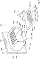
- FIG 1 an assembled state of the dummy plug 12a is shown, in which the dummy plug 12a is plugged into the mating data plug unit 16a.
- the figures 2 and 3 each show a detailed structure of the dummy plug 12a. While in the figure 2 Explicitly only one housing unit 46a of the blind plug 12a can be seen figure 3 the housing unit 46a and a circuit board 24a of the data connector unit 14a. In addition, you can figures 4 and 5 Detailed views of the circuit board 24a are removed, the figure 6 shows a schematic of circuit board 24a.
- the housing unit 46a has at least one cover element 52a so that the dummy plug 12a functions as a protection against dust. Once again figure 1 it can be seen that the cover element 52a covers the mating data connector unit 16a flush with the surface.
- the cover member 52a defines a front wall of the housing unit 46a.
- the housing unit 46a also has two side walls 54a, 56a, which are arranged perpendicularly on the cover element 52a. On a side of the side walls 54a, 56a facing away from the cover element 52a, the housing unit 46a has a rear wall 58a.
- the rear wall 58a delimits a depth direction of the housing unit 46a starting from the cover element 52a and is also arranged perpendicularly on the side walls 54a, 56a.
- the rear wall 58a and the cover element 52a extend at least essentially parallel to one another.
- the housing unit 46a has a bottom wall 60a.
- Bottom wall 60a is perpendicular to side walls 54a, 56a and perpendicular to cover member 52a and back wall 58a, respectively.
- the figures 2 and 3 show that the cover member 52a with the side walls 54a, 56a, the back wall 58a and the bottom wall 60a define a cavity 48a.
- the housing unit 46a is formed in one piece and is manufactured in one piece in a manufacturing process by means of an injection molding method.
- the housing unit 46a has at least one fixing element 50a for fixing the data plug unit 14a to the mating data plug unit 16a.
- the fixing element 50a is arranged on a respective upper side 96a, 98a of the side walls 54a, 56a facing away from the bottom wall 60a.
- the fixing element 50a is connected to the side 96a, 98a and a side 100a of the covering element which faces the rear wall 58a 52a connected to the cover member 52a.
- the fixing element 50a is provided to produce a clamping effect of the data connector unit 14a with the mating data connector unit 16a in the assembled state.
- the housing unit 46a has a recess 72a on an upper edge 110a of the cover element 52a facing the mating data plug unit 16a.
- the housing unit 46a has a further recess 74a on a lower edge 112a of the cover element 52a facing the mating data connector unit 16a.
- the upper edge 110a and the lower edge 112a are located on the side 100a of the cover element 52a facing the rear wall 58a.
- the figure 1 shows a section of the upper edge 110a and the lower edge 112a with the recess 72a and the further recess 74a.
- the side walls 54a, 56a each have a step 64a on a side facing the cavity 48a.
- an extension height of the step 64a is equal to an extension height of the rear wall 58a.
- a side 114a of the step 64a facing away from the bottom wall 60a and a side 116a of the back wall 58a facing away from the bottom wall 60a consequently lie in one plane, being arranged perpendicularly to one another.
- a guide element 62a of the housing unit 46a is arranged on the side walls 54a, 56a on the side facing the cavity 48a.
- the guide element 62a is integrally connected to the side wall 54a, 56a on a side 66a facing the side wall 54a, 56a.
- the guide element 62a extends over an extension height of the side 96a, 98a of the side wall 54a, 56a facing away from the bottom wall 60a and protrudes beyond these sides 96a, 98a.
- the guide element 62a is provided for correct positioning with the housing unit 46a when the printed circuit board 24a is inserted.
- the printed circuit board 24a has a pilot hole 124a in each case on a side 120a, 122a facing the side walls 54a, 56a.
- the guide member 62a is adapted to a shape of the pilot hole 124a.
- the housing unit 46a and the circuit board 24a are above the Pilot hole 124a and the guide element 62a connected to each other.
- the pilot hole 124a is intended to fix the printed circuit board 24a to the housing unit 46a with the guide element 62a.
- the data plug unit 14a has at least one output unit 18a for displaying a power supply capacity of the mating data plug unit 16a.
- the output unit 18a is connected to the circuit board 24a for an electrical supply.
- the printed circuit board 24a is inserted with an underside 78a of the printed circuit board 24a along a mounting direction 118a into the housing unit 46a.
- the housing unit 46a and the underside 78a of the printed circuit board 24a thus together form the at least essentially closed cavity 48a.
- the housing unit 46a is intended to accommodate the dispensing unit 18a.
- the output unit 18a is arranged on the underside 78a of the printed circuit board 24a.
- the output unit 18a is positioned in the cavity 48a.
- the output unit 18a has at least one light source designed as an LED 20a.
- the output unit 18a has at least one additional LED 22a as an additional light source.
- the LED 20a and the further LED 22a are arranged on the underside 78a of the printed circuit board 24a. The LED 20a and the further LED 22a are thus located in at least the cavity 48a in the assembled state.
- the housing unit 46a is designed to be at least partially transparent in order to display the power supply capacity of the mating data connector unit 16a by means of the LED 20a and the further LED 22a.
- the printed circuit board 24a has contacts 101a, 102a, 103a, 104a, 105a, 106a, 107a, 108a for contacting with mating contacts (not shown) of the mating data plug unit 16a.
- the contacts 101a, 102a, 103a, 104a, 105a, 106a, 107a, 108a are arranged in indentations on a side 26a facing the mating data connector unit 16a.
- the printed circuit board 24a has at least one first conductive path 28a, which electrically conductively connects at least a first of the contacts 101a, 102a to a first terminal 30a of the LED 20a.
- the printed circuit board 24a has a second conductive path 32a, which electrically conductively connects at least a second of the contacts 103a, 106a to a second terminal 34a of the LED 20a.
- the LED 20a is electrically conductively connected to at least two of the contacts 101a, 102a, 103a, 106a by means of the first conductive path 28a and by means of the second conductive path 32a (cf. figure 5 ).
- the printed circuit board 24a has at least one further first conduction path 36a, which electrically conductively connects at least one further first of the contacts 107a, 108a to a further first terminal 38a of the further LED 22a.
- the printed circuit board 24a has a further second conduction path 40a, which electrically conductively connects at least one further second of the contacts 104a, 105a to a further second connection 42a of the further LED 22a.
- the additional LED 22a is thus electrically conductively connected via the additional first conduction path 36a and the additional second conduction path 40a to at least two additional contacts 104a, 105a, 107a, 108a (cf. figure 5 ).
- first connection 30a, the second connection 34a, the further first connection 38a and the further second connection 42a are arranged on the underside 78a of the printed circuit board 24a.
- the illustrated scheme of the circuit board 24a shows that the first conduction path 28a has a first conduction path section 80a and an additional first conduction path section 82a.
- the first conduction path section 80a is connected to the first contact 101a and the additional first conduction path section 82a is connected to the one additional first contact 102a.
- the first contact 101a and the additional first contact 102a are adjacent.
- the second conduction path 32a also has a second conduction path section 84a and an additional second conduction path section 90a.
- the second conduction path section 84a is connected to the second contact 103a and the additional second conduction path section 90a to the one additional second contact 106a.
- the figures 4 and 6 show that the first conductive path portion 80a is shorted to the additional first conductive path portion 82a on the top surface 76a of the printed circuit board 24a.
- the second line path section 84a is also included shorted to the additional second conduction path section 90a on the top side 76a of the printed circuit board 24a.
- the further first conduction path 36a has a further first conduction path section 92a and a further additional first conduction path section 94a.
- the further first conduction path section 92a is connected to the further first contact 107a and the further additional first conduction path section 94a is connected to the one further additional first contact 108a.
- the further first contact 107a and the further additional first contact 108a are adjacent.
- the further second conduction path 40a likewise has a further second conduction path section 86a and a further additional second conduction path section 88a.
- the further second conduction path section 86a is connected to the further second contact 104a and the further additional second conduction path section 88a to the one further additional second contact 105a.
- the further second contact 104a and the further additional second contact 105a are arranged adjacently.
- the figures 4 and 6 show that the further first conduction path section 92a is short-circuited to the further additional first conduction path section 94a on the upper side 76a of the printed circuit board 24a.
- the figures 4 and 6 it can be seen that the further second conduction path section 86a is short-circuited with the further additional second conduction path section 88a on the upper side 76a of the printed circuit board 24a.
- the first conductive path 28a and the second conductive path 32a and the further first conductive path 36a and the further second conductive path 40a run over an edge 44a of the printed circuit board 24a to establish an electrical connection between the upper side 76a of the printed circuit board 24a and the lower side 78a of the printed circuit board 24a.
- the edge 44a is located on the side 26a of the printed circuit board 24a facing the mating data connector unit 16a.
- the figure 7 shows a dummy plug 12b of a further embodiment.
- the dummy plug 12b has a data plug unit 14b with at least one printed circuit board 24b.
- the dummy plug 12b has a housing unit 46b.
- the circuit board 24b is connected to the housing unit 46b.
- the dummy plug 12b of the present exemplary embodiment differs from the dummy plug 12a of exemplary embodiment a at least in one arrangement and/or connection of the printed circuit board 24b with and/or on the housing unit 46b.
- the printed circuit board 24b is plugged into the housing unit 46b parallel to a plug-in direction.
- figure 7 illustrates a mounting direction 118b, which runs parallel to the plug-in direction.
- the printed circuit board 24b is inserted into the housing unit 46b along the mounting direction 118b.
- the housing unit 46b has at least one guide bar 132b. Furthermore, the housing unit 46b has a further guide web 136b arranged opposite the guide web 132b.
- the printed circuit board 24b is inserted into the housing unit 46b along the guide web 132b and the further guide web 136b (cf. Figures 8 to 10 ). In a mounted state, the printed circuit board 24b rests on the guide web 132b and the further guide web 136b.
- the Figures 7 to 10 it can be seen that an area below the circuit board 24b and inside the housing unit 46b is presently empty. Alternatively, this area could also be at least partially filled with at least one material and/or a material composition, such as plastic and/or resin and/or a composite material.
- the housing unit 46b has at least one light guide 126b, which deflects a beam path at least once (cf. Figures 9 and 10 ).
- the housing unit 46b forms the light guide 126b.
- the data connector unit 14b includes an output unit 18b, which has at least one light source 20b.
- the output unit 18b has at least one additional light source 22b.
- circuit board 24b is arranged in housing unit 46b in such a way that at least illuminant 20b and/or the additional illuminant 22b is/are aligned at least substantially perpendicular to an entry region 138b of light guide 126b (see. figure 10 ).
- the entry area 138b of the light guide 126b is adapted to a dimension and/or shape and/or size of the illuminant 20b and/or the further illuminant 22b.
- the light guide 126b is intended to guide the light provided by the illuminant 20b and/or the additional illuminant 22b directly and in this case unprocessed in the direction of at least one front side 128b of the housing unit 46b (cf. figure 10 ).
- the dummy plug 12b of the present exemplary embodiment differs from the dummy plug 12a of exemplary embodiment a by a different configuration of a fixing element 50b of housing unit 46b.
- the fixing element 50b is designed as a detent lever 140b (cf. Figures 7 to 10 ).
- the fixing element 50b is intended to produce a clamping effect and/or latching connection of the data plug unit 14b with a mating data plug unit (not shown) in the assembled state.
Landscapes
- Engineering & Computer Science (AREA)
- Microelectronics & Electronic Packaging (AREA)
- Physics & Mathematics (AREA)
- Optics & Photonics (AREA)
- Manufacturing & Machinery (AREA)
- General Physics & Mathematics (AREA)
- Details Of Connecting Devices For Male And Female Coupling (AREA)
Applications Claiming Priority (1)
| Application Number | Priority Date | Filing Date | Title |
|---|---|---|---|
| DE102020128513.2A DE102020128513A1 (de) | 2020-10-29 | 2020-10-29 | Blindstecker und Verfahren zur Anzeige einer Stromversorgungskapazität |
Publications (1)
| Publication Number | Publication Date |
|---|---|
| EP3993171A1 true EP3993171A1 (fr) | 2022-05-04 |
Family
ID=78413788
Family Applications (1)
| Application Number | Title | Priority Date | Filing Date |
|---|---|---|---|
| EP21204972.0A Pending EP3993171A1 (fr) | 2020-10-29 | 2021-10-27 | Connecteur enfichable aveugle, système de transfert de données et procédé d'affichage d'une capacité d'alimentation électrique |
Country Status (3)
| Country | Link |
|---|---|
| US (1) | US12191610B2 (fr) |
| EP (1) | EP3993171A1 (fr) |
| DE (1) | DE102020128513A1 (fr) |
Families Citing this family (2)
| Publication number | Priority date | Publication date | Assignee | Title |
|---|---|---|---|---|
| US11916327B2 (en) * | 2021-08-10 | 2024-02-27 | Dell Products L.P. | Space-optimized cable connector interface |
| CN217522314U (zh) * | 2022-05-11 | 2022-09-30 | 景霞荣 | 一种用于插头或插座的旋转手柄 |
Citations (4)
| Publication number | Priority date | Publication date | Assignee | Title |
|---|---|---|---|---|
| US5692925A (en) * | 1986-07-23 | 1997-12-02 | Virginia Patent Development Corporation | Modular plug comprising circuit elements |
| WO2000017968A1 (fr) * | 1998-09-24 | 2000-03-30 | Xircom, Inc. | Indicateur d'etat pour un dispositif electronique |
| US20120270436A1 (en) * | 2011-04-19 | 2012-10-25 | Blythe Stephen P | Identifying individual copper network cables on a patch panel |
| GB2527310A (en) * | 2014-06-17 | 2015-12-23 | Andrew Alphonso Robotham | Patchmate cable tracer and continuity tester |
Family Cites Families (7)
| Publication number | Priority date | Publication date | Assignee | Title |
|---|---|---|---|---|
| US7384300B1 (en) * | 1999-12-22 | 2008-06-10 | Xerox Corporation | Method and apparatus for a connection sensing apparatus |
| US8113721B1 (en) * | 2009-06-12 | 2012-02-14 | Applied Micro Circuits Corporation | Off-axis misalignment compensating fiber optic cable interface |
| US8376760B1 (en) * | 2011-01-27 | 2013-02-19 | Physical Optics Corporation | Avionics data storage device and transfer system with electro-opto-mechanical identification |
| CN107706685B (zh) * | 2017-11-24 | 2024-06-18 | 深圳市乐得瑞科技有限公司 | 一种连接器 |
| US11038307B2 (en) * | 2018-05-25 | 2021-06-15 | Cisco Technology, Inc. | Cable power rating identification for power distribution over communications cabling |
| US10754103B2 (en) * | 2018-10-08 | 2020-08-25 | Hewlett Packard Enterprise Development Lp | Universal-blindmate sleeve and blindmate connectors |
| US11689247B2 (en) * | 2019-01-16 | 2023-06-27 | Mertek Industries, Llc | Patch cord including wireless components |
-
2020
- 2020-10-29 DE DE102020128513.2A patent/DE102020128513A1/de not_active Withdrawn
-
2021
- 2021-10-27 US US17/511,809 patent/US12191610B2/en active Active
- 2021-10-27 EP EP21204972.0A patent/EP3993171A1/fr active Pending
Patent Citations (4)
| Publication number | Priority date | Publication date | Assignee | Title |
|---|---|---|---|---|
| US5692925A (en) * | 1986-07-23 | 1997-12-02 | Virginia Patent Development Corporation | Modular plug comprising circuit elements |
| WO2000017968A1 (fr) * | 1998-09-24 | 2000-03-30 | Xircom, Inc. | Indicateur d'etat pour un dispositif electronique |
| US20120270436A1 (en) * | 2011-04-19 | 2012-10-25 | Blythe Stephen P | Identifying individual copper network cables on a patch panel |
| GB2527310A (en) * | 2014-06-17 | 2015-12-23 | Andrew Alphonso Robotham | Patchmate cable tracer and continuity tester |
Also Published As
| Publication number | Publication date |
|---|---|
| DE102020128513A1 (de) | 2022-05-05 |
| US12191610B2 (en) | 2025-01-07 |
| US20220140546A1 (en) | 2022-05-05 |
Similar Documents
| Publication | Publication Date | Title |
|---|---|---|
| DE60128235T2 (de) | Drahtverbinder | |
| DE10212895A1 (de) | Signalsäule | |
| EP4089852B1 (fr) | Prise modulaire de courant et procédé de paramétrage / installation automatique | |
| DE102015117486A1 (de) | Organische Leuchtdiode und Anordnung mit einer organischen Leuchtdiode | |
| EP3819999A1 (fr) | Connecteur enfichable à encastrer | |
| DE102020128513A1 (de) | Blindstecker und Verfahren zur Anzeige einer Stromversorgungskapazität | |
| DE102013207006A1 (de) | System und Verfahren zum Verifizieren der Montage eines Verbinders | |
| DE202008017697U1 (de) | Steckverbinder und Steckbuchse für Telekommunikations- oder Datenkabel | |
| EP3741011B1 (fr) | Dispositif de protection pour ensemble de raccordement par enfichage | |
| DE102020110237B4 (de) | Steckverbinderanordnung und verfahren zur herstellung einer steckverbinderanordnung | |
| DE102008060430B4 (de) | Steckverbindergehäuse mit Lichtleitelement | |
| DE102015101796A1 (de) | Lichtemittierendes Modul und dieses verwendende Beleuchtungseinrichtung | |
| DE102010043295B4 (de) | Lichtemittermodul | |
| DE202014105629U1 (de) | LED-Lampe | |
| DE19521735A1 (de) | Fahrzeugleuchte mit verbesserter Steckelementstruktur | |
| DE102010043296A1 (de) | Lichtemittermodul mit Umlenkoptik | |
| EP2196982B1 (fr) | Afficheur segmenté doté d'un guide de lumière | |
| DE10316512A1 (de) | Signalgerät | |
| DE102016117099A1 (de) | Gurtschloss mit Beleuchtung | |
| EP3729152A2 (fr) | Système formant connecteur enfichable | |
| DE202024103976U1 (de) | Ladekabel | |
| WO1987004771A1 (fr) | Lampe fluorescente | |
| DE102014208173A1 (de) | Einrichtungen und Anordnungen zum berührungslosen Erfassen eines Tastenknopfhubes, Verfahren zum Herstellen einer solchen Einrichtung und Verfahren zum berührungslosen Erfassen eines Tastenknopfhubes | |
| DE112017003554T5 (de) | Leuchtvorrichtung unter Verwendung eines drahtlosen Leistungsübertragungsmoduls | |
| DE102018129122A1 (de) | Ladesteckverbinder mit einem Streuelement zum Abstrahlen und/oder Empfangen von Licht |
Legal Events
| Date | Code | Title | Description |
|---|---|---|---|
| PUAI | Public reference made under article 153(3) epc to a published international application that has entered the european phase |
Free format text: ORIGINAL CODE: 0009012 |
|
| STAA | Information on the status of an ep patent application or granted ep patent |
Free format text: STATUS: THE APPLICATION HAS BEEN PUBLISHED |
|
| AK | Designated contracting states |
Kind code of ref document: A1 Designated state(s): AL AT BE BG CH CY CZ DE DK EE ES FI FR GB GR HR HU IE IS IT LI LT LU LV MC MK MT NL NO PL PT RO RS SE SI SK SM TR |
|
| STAA | Information on the status of an ep patent application or granted ep patent |
Free format text: STATUS: REQUEST FOR EXAMINATION WAS MADE |
|
| 17P | Request for examination filed |
Effective date: 20221028 |
|
| RBV | Designated contracting states (corrected) |
Designated state(s): AL AT BE BG CH CY CZ DE DK EE ES FI FR GB GR HR HU IE IS IT LI LT LU LV MC MK MT NL NO PL PT RO RS SE SI SK SM TR |
|
| STAA | Information on the status of an ep patent application or granted ep patent |
Free format text: STATUS: EXAMINATION IS IN PROGRESS |
|
| 17Q | First examination report despatched |
Effective date: 20231129 |