EP3993262A1 - Funkgerät - Google Patents
Funkgerät Download PDFInfo
- Publication number
- EP3993262A1 EP3993262A1 EP21204635.3A EP21204635A EP3993262A1 EP 3993262 A1 EP3993262 A1 EP 3993262A1 EP 21204635 A EP21204635 A EP 21204635A EP 3993262 A1 EP3993262 A1 EP 3993262A1
- Authority
- EP
- European Patent Office
- Prior art keywords
- gain
- amplifiers
- dpd
- signal
- input
- Prior art date
- Legal status (The legal status is an assumption and is not a legal conclusion. Google has not performed a legal analysis and makes no representation as to the accuracy of the status listed.)
- Pending
Links
Images




Classifications
-
- H—ELECTRICITY
- H03—ELECTRONIC CIRCUITRY
- H03F—AMPLIFIERS
- H03F3/00—Amplifiers with only discharge tubes or only semiconductor devices as amplifying elements
- H03F3/72—Gated amplifiers, i.e. amplifiers which are rendered operative or inoperative by means of a control signal
-
- H—ELECTRICITY
- H04—ELECTRIC COMMUNICATION TECHNIQUE
- H04B—TRANSMISSION
- H04B1/00—Details of transmission systems, not covered by a single one of groups H04B3/00 - H04B13/00; Details of transmission systems not characterised by the medium used for transmission
- H04B1/62—Details of transmission systems, not covered by a single one of groups H04B3/00 - H04B13/00; Details of transmission systems not characterised by the medium used for transmission for providing a predistortion of the signal in the transmitter and corresponding correction in the receiver, e.g. for improving the signal/noise ratio
-
- H—ELECTRICITY
- H03—ELECTRONIC CIRCUITRY
- H03F—AMPLIFIERS
- H03F1/00—Details of amplifiers with only discharge tubes, only semiconductor devices or only unspecified devices as amplifying elements
- H03F1/32—Modifications of amplifiers to reduce non-linear distortion
- H03F1/3241—Modifications of amplifiers to reduce non-linear distortion using predistortion circuits
-
- H—ELECTRICITY
- H03—ELECTRONIC CIRCUITRY
- H03F—AMPLIFIERS
- H03F1/00—Details of amplifiers with only discharge tubes, only semiconductor devices or only unspecified devices as amplifying elements
- H03F1/32—Modifications of amplifiers to reduce non-linear distortion
- H03F1/3241—Modifications of amplifiers to reduce non-linear distortion using predistortion circuits
- H03F1/3247—Modifications of amplifiers to reduce non-linear distortion using predistortion circuits using feedback acting on predistortion circuits
-
- H—ELECTRICITY
- H03—ELECTRONIC CIRCUITRY
- H03F—AMPLIFIERS
- H03F3/00—Amplifiers with only discharge tubes or only semiconductor devices as amplifying elements
- H03F3/189—High-frequency amplifiers, e.g. radio frequency amplifiers
- H03F3/19—High-frequency amplifiers, e.g. radio frequency amplifiers with semiconductor devices only
-
- H—ELECTRICITY
- H03—ELECTRONIC CIRCUITRY
- H03F—AMPLIFIERS
- H03F3/00—Amplifiers with only discharge tubes or only semiconductor devices as amplifying elements
- H03F3/189—High-frequency amplifiers, e.g. radio frequency amplifiers
- H03F3/19—High-frequency amplifiers, e.g. radio frequency amplifiers with semiconductor devices only
- H03F3/195—High-frequency amplifiers, e.g. radio frequency amplifiers with semiconductor devices only in integrated circuits
-
- H—ELECTRICITY
- H03—ELECTRONIC CIRCUITRY
- H03F—AMPLIFIERS
- H03F3/00—Amplifiers with only discharge tubes or only semiconductor devices as amplifying elements
- H03F3/20—Power amplifiers, e.g. Class B amplifiers, Class C amplifiers
- H03F3/21—Power amplifiers, e.g. Class B amplifiers, Class C amplifiers with semiconductor devices only
- H03F3/213—Power amplifiers, e.g. Class B amplifiers, Class C amplifiers with semiconductor devices only in integrated circuits
-
- H—ELECTRICITY
- H03—ELECTRONIC CIRCUITRY
- H03F—AMPLIFIERS
- H03F3/00—Amplifiers with only discharge tubes or only semiconductor devices as amplifying elements
- H03F3/20—Power amplifiers, e.g. Class B amplifiers, Class C amplifiers
- H03F3/24—Power amplifiers, e.g. Class B amplifiers, Class C amplifiers of transmitter output stages
- H03F3/245—Power amplifiers, e.g. Class B amplifiers, Class C amplifiers of transmitter output stages with semiconductor devices only
-
- H—ELECTRICITY
- H04—ELECTRIC COMMUNICATION TECHNIQUE
- H04B—TRANSMISSION
- H04B1/00—Details of transmission systems, not covered by a single one of groups H04B3/00 - H04B13/00; Details of transmission systems not characterised by the medium used for transmission
- H04B1/005—Details of transmission systems, not covered by a single one of groups H04B3/00 - H04B13/00; Details of transmission systems not characterised by the medium used for transmission adapting radio receivers, transmitters andtransceivers for operation on two or more bands, i.e. frequency ranges
-
- H—ELECTRICITY
- H04—ELECTRIC COMMUNICATION TECHNIQUE
- H04B—TRANSMISSION
- H04B1/00—Details of transmission systems, not covered by a single one of groups H04B3/00 - H04B13/00; Details of transmission systems not characterised by the medium used for transmission
- H04B1/005—Details of transmission systems, not covered by a single one of groups H04B3/00 - H04B13/00; Details of transmission systems not characterised by the medium used for transmission adapting radio receivers, transmitters andtransceivers for operation on two or more bands, i.e. frequency ranges
- H04B1/0067—Details of transmission systems, not covered by a single one of groups H04B3/00 - H04B13/00; Details of transmission systems not characterised by the medium used for transmission adapting radio receivers, transmitters andtransceivers for operation on two or more bands, i.e. frequency ranges with one or more circuit blocks in common for different bands
- H04B1/0075—Details of transmission systems, not covered by a single one of groups H04B3/00 - H04B13/00; Details of transmission systems not characterised by the medium used for transmission adapting radio receivers, transmitters andtransceivers for operation on two or more bands, i.e. frequency ranges with one or more circuit blocks in common for different bands using different intermediate frequencied for the different bands
- H04B1/0078—Details of transmission systems, not covered by a single one of groups H04B3/00 - H04B13/00; Details of transmission systems not characterised by the medium used for transmission adapting radio receivers, transmitters andtransceivers for operation on two or more bands, i.e. frequency ranges with one or more circuit blocks in common for different bands using different intermediate frequencied for the different bands with a common intermediate frequency amplifier for the different intermediate frequencies, e.g. when using switched intermediate frequency filters
-
- H—ELECTRICITY
- H04—ELECTRIC COMMUNICATION TECHNIQUE
- H04B—TRANSMISSION
- H04B1/00—Details of transmission systems, not covered by a single one of groups H04B3/00 - H04B13/00; Details of transmission systems not characterised by the medium used for transmission
- H04B1/02—Transmitters
- H04B1/04—Circuits
- H04B1/0458—Arrangements for matching and coupling between power amplifier and antenna or between amplifying stages
-
- H—ELECTRICITY
- H04—ELECTRIC COMMUNICATION TECHNIQUE
- H04B—TRANSMISSION
- H04B1/00—Details of transmission systems, not covered by a single one of groups H04B3/00 - H04B13/00; Details of transmission systems not characterised by the medium used for transmission
- H04B1/02—Transmitters
- H04B1/04—Circuits
- H04B1/0475—Circuits with means for limiting noise, interference or distortion
-
- H—ELECTRICITY
- H04—ELECTRIC COMMUNICATION TECHNIQUE
- H04B—TRANSMISSION
- H04B1/00—Details of transmission systems, not covered by a single one of groups H04B3/00 - H04B13/00; Details of transmission systems not characterised by the medium used for transmission
- H04B1/02—Transmitters
- H04B1/04—Circuits
- H04B1/0483—Transmitters with multiple parallel paths
-
- H—ELECTRICITY
- H03—ELECTRONIC CIRCUITRY
- H03F—AMPLIFIERS
- H03F2200/00—Indexing scheme relating to amplifiers
- H03F2200/111—Indexing scheme relating to amplifiers the amplifier being a dual or triple band amplifier, e.g. 900 and 1800 MHz, e.g. switched or not switched, simultaneously or not
-
- H—ELECTRICITY
- H03—ELECTRONIC CIRCUITRY
- H03F—AMPLIFIERS
- H03F2200/00—Indexing scheme relating to amplifiers
- H03F2200/451—Indexing scheme relating to amplifiers the amplifier being a radio frequency amplifier
-
- H—ELECTRICITY
- H03—ELECTRONIC CIRCUITRY
- H03F—AMPLIFIERS
- H03F2203/00—Indexing scheme relating to amplifiers with only discharge tubes or only semiconductor devices as amplifying elements covered by H03F3/00
- H03F2203/72—Indexing scheme relating to gated amplifiers, i.e. amplifiers which are rendered operative or inoperative by means of a control signal
- H03F2203/7209—Indexing scheme relating to gated amplifiers, i.e. amplifiers which are rendered operative or inoperative by means of a control signal the gated amplifier being switched from a first band to a second band
-
- H—ELECTRICITY
- H04—ELECTRIC COMMUNICATION TECHNIQUE
- H04B—TRANSMISSION
- H04B1/00—Details of transmission systems, not covered by a single one of groups H04B3/00 - H04B13/00; Details of transmission systems not characterised by the medium used for transmission
- H04B1/02—Transmitters
- H04B1/04—Circuits
- H04B2001/0408—Circuits with power amplifiers
-
- H—ELECTRICITY
- H04—ELECTRIC COMMUNICATION TECHNIQUE
- H04B—TRANSMISSION
- H04B1/00—Details of transmission systems, not covered by a single one of groups H04B3/00 - H04B13/00; Details of transmission systems not characterised by the medium used for transmission
- H04B1/02—Transmitters
- H04B1/04—Circuits
- H04B2001/0408—Circuits with power amplifiers
- H04B2001/0425—Circuits with power amplifiers with linearisation using predistortion
Definitions
- Embodiments relate to a radio apparatus and signal processing methods for the radio apparatus.
- an apparatus comprising means for: providing two or more amplifiers for amplifying signals in two or more respective frequency bands; receiving a composite signal comprising first and second predistorted input signals in first and second frequency bands; filtering the composite signal to provide (i) the first predistorted signal for input to a first amplifier of the two or more amplifiers for producing an amplified first output signal and (ii) the second predistorted signal for input to a second amplifier of the two or more amplifiers for producing an amplified second output signal; routing, at non-overlapping times, the first and second output signals to a common feedback path; and linearizing received first and second input signals based on the respective first and second output signals received on the common feedback path.
- the linearizing means may comprise first and second DPDs for applying a predistortion to the respective first and second input signals prior to combining, wherein the routing means is configured to route either the first output signal to the first DPD or to route the second output signal to the second DPD.
- Each of the first and second DPDs may comprise first and second sub-models defined by first and second DPD filters, the first and second sub-models being configured to predistort respective first and second subsets of frequency components of the input signal.
- a technical effect may be to minimize effects to the DPDs due to significant group delay.
- the apparatus may further comprise: a common gain controller for controlling the gain of the composite signal; and first and second post-scaling controllers for individually controlling the gain of the respective first and second input signals subsequent to predistortion by the respective first and second DPDs.
- the apparatus may further comprise means for determining residual first and second gain errors associated with the first and second input signals subsequent to applying the common gain adjustment value.
- the apparatus may further comprise means for determining and applying individual gain adjustment values for the respective first and second post-scaling controllers to reduce or substantially remove the residual first and second gain errors.
- the apparatus may further comprise means for clipping the respective first and second input signals prior to mixing so as not to exceed a predetermined peak to average value.
- the two or more amplifiers may be power amplifiers for connection to a common antenna.
- the apparatus may comprise a radio module for a radio access network base station.
- a method comprising: routing, at non-overlapping times, first and second output signals from respective first and second amplifiers to a common feedback path, the first and second amplifiers being for amplifying signals in two or more respective frequency bands; and causing linearizing of received first and second input signals for the first and second amplifiers.
- the routing may be performed by controlling a digital switch.
- the linearizing may comprise use of one or more digital predistorters (DPDs).
- DPDs digital predistorters
- Each of the first and second DPDs may comprise first and second sub-models defined by first and second DPD filters, the first and second sub-models being configured to predistort respective first and second subsets of frequency components of the input signal.
- the technical effect may be to minimize effects to the DPDs due to significant group delay.
- the first and second DPD filters may be complementary half-band filters.
- the method may further comprise: controlling a common gain controller for controlling the gain of the composite signal; and controlling first and second post-scaling controllers for individually controlling the gain of the respective first and second input signals subsequent to predistortion by the respective first and second DPDs.
- the method may further comprise determining residual first and second gain errors associated with the first and second input signals subsequent to applying the common gain adjustment value.
- the method may comprise controlling the first and second post-scaling controllers by determining and applying individual gain adjustment values for the respective first and second post-scaling controllers to reduce or substantially remove the residual first and second gain errors.
- a computer program product comprising a set of instructions which, when executed on an apparatus, is configured to cause the apparatus to carry out the method of any preceding method definition.
- a non-transitory computer readable medium comprising program instructions stored thereon for performing a method, comprising: routing, at non-overlapping times, first and second output signals from respective first and second amplifiers to a common feedback path, the first and second amplifiers being for amplifying signals in two or more respective frequency bands; and causing linearizing of received first and second input signals for the first and second amplifiers.
- a radio apparatus may be referred to herein as a radio frequency module (RFM).
- RFMs may be installed by a radio access network (RAN) operator at each of one or more base stations.
- a RFM may be considered self-contained unit comprising digital and analogue components for receiving and processing baseband input signals for coding, modulation and amplification via one or more power amplifiers, and transmission via an antenna connected to an output port of the apparatus.
- the RFM may also be configured to receive RF signals for demodulation although this disclosure may focus on the transmission chain.
- the antenna may be local or remote to the RFM.
- the RFM may be connected to the antenna via a fibre cable for remote situations.
- PA diplexed power amplifier
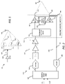
- the RFM 110 may comprise a digital front end (DFE) 112.
- DFE digital front end
- the DFE 112 may comprise one or more digital processing modules, for example one or more Field Programmable Gate Arrays (FPGAs), Application Specific Integrated Circuits (ASICs) or any one or more processors or controllers configured to perform digital signal processing (DSP) operations on respective input signals x1 , x2 to be transmitted on the two or more different bands.
- FPGAs Field Programmable Gate Arrays
- ASICs Application Specific Integrated Circuits
- DSP digital signal processing
- DSP operations may comprise encoding and/or modulation of input signals using carriers appropriate for the respective bands.
- the DFE 112 may also sum or combine the first and second predistorted and modulated signals x1 , x2 to provide the composite signal x which forms an output of the DFE 112.
- the composite signal x is provided to an RF Digital to Analogue Converter (DAC) 114, a LPTX stage 115, and then, as shown in FIG. 2 , a so-called frequency selective amplifier 116.
- DAC Digital to Analogue Converter
- the frequency selective amplifier 116 may comprise a so-called frequency selective block (FSB) 120 which may be a diplexer such as that indicated in the FIG. 1 topology, including bandpass filters appropriate to the required first and second (and any additional) bands.
- FFB frequency selective block
- a power supply 126 may provide one or more of d.c. and bias voltages to the first and second PAs 122, 124. Their values may be independent of one another. For example, the power supply 126 may provide a certain drain voltage (VDD1) to the first PA 122 and the same or a different drain voltage (VDD2) to the second PA 124. For example, the power supply 126 may provide a certain gate bias voltage (Vgsi) to the first PA 122 and the same or a different gate voltage (Vgs2) to the second PA 124.
- VDD1 drain voltage
- VDD2 drain voltage
- Vgsi gate bias voltage
- the outputs of the first and second PAs 122, 134 may also be fed-back to the DFE 112 using a common feedback line 141, via an RF Analogue to Digital Converter (ADC) 142, to provide a reference signal for the DPD as mentioned above.
- ADC Analogue to Digital Converter
- a switch 146 may be provided for this purpose, for example configured so that only one respective output of the first and second PAs 122, 124 is connected to the common feedback line 141 at a given time.
- FIG. 3 is a block diagram showing some components of the DFE 112.
- the common feedback line 141 provides a reference signal to the DPD 302 from, at a particular time, one of the first and second PAs 122, 124.
- a reference signal based on the output of the first PA 122 is compared with the corresponding input signal x1 to determine, in effect, the transfer function of the first PA.
- This may generate a first DPD model.
- a reference signal based on the output of the second PA 124 is compared with the corresponding input signal x2 to determine, in effect, the transfer function of the second PA. This may generate a second DPD model.
- first and second post scalers 340, 350 and the WA 360 are explained below.
- the DFE 112 may also comprise a controller 304.
- the controller 304 may be a dedicated processor separate from the DFE 112.
- the controller 304 may be configured by means of hardware, software or firmware to perform certain processing functions within, or in association with, the RFM 110.
- the composite signal x comprises two sub-band signals, for example x1 for band 25 and x2 for band 66 etc.
- the composite signal x may consist of n components for an n band multiplex design.
- x1 and x2 are two separate signals. x1 and x2 are clipped to a specified PAR threshold.
- a routing means such as a switch 146 may be provided for this purpose.
- the switch may, for example, be configured such that only one respective output of the first and second PAs 122, 124 is connected to the common feedback line 141 at a given time. Put another way, the outputs of the first and second PAs 122, 124 are routed, at non-overlapping times, to the common feedback line 141.
- the diplexer filters of the FSB 120 needs to cover frequencies where DPD correction is desired. This may include the transmit band and the receive band where significant transmit IM products fall, usually to one side of IM3.
- the diplexer filters also need to reject the other transmit bands sufficiently. This poses a significant problem for cases where the transmit bands are close to each other. Specifically, B25/B66 is one such example where the large rejection of the other transmit band does not lend itself to cover the frequencies between B25 and B66.
- B25 upper-side IM products will largely be in the roll-off region, or the rejection region of the B25 filter
- B66 lower-side IM products will largely be in the roll-off region, or the rejection region of the B66 filter.
- the first and second DPD engines 302A, 302B then will not attempt to generate a predistortion signal in between the B25 and B66 frequencies, except for a small region immediately adjacent to them. This means that, if we consider the predistortion signal at the input of the diplexer, focusing on the region between the B25 and B66 frequencies, we will only see significant frequency components close to each transmit band. No correction will be anticipated for a large part of the frequencies in-between the bands.
- Equation (2) is the basis of a single-band DPD model, commonly used in the industry. The following paragraphs describe equation (2) with limited terms.
- Equations (3) to (5) describe the split band DPD engine in accordance with example embodiments.
- each column in the matric X as a signal can be filtered to generate another signal of the same length. Since filtering is a linear operation on signals, it can be represented by a linear function.
- a linear function on a signal of finite length can be represented by a matrix, and consequently all the usual matrix operations will apply.
- filters may be applied to each column of X .
- a primary candidate for the filters f 1 and f 2 are complementary half-band filters.
- complementary filters there are other forms of complementary filters as well, which are power and magnitude based complementary forms and are also applicable herein.
- complementary filters can be complex, achieving a split which can occur at any point in the frequency axis.
- X 1 the matrix associated with split band 1. Note how the non-linear terms are filtered with the complementary filter f 1 . Filtering occurs on the time domain samples per each term (per column).
- the least square problem is: X 1 ⁇ 1 ⁇ y 1
- the least square problem is: X 2 ⁇ 2 ⁇ y 2
- the example above shows a single band can be split into two independent DPD engines. Both DPD split bands are solved independently thus, accommodating a wider frequency span to two smaller frequency spans.
- the matrices X 1 and X 2 can be combined to a single matrix, thus solving for both engines at once.
- the diplexer may be configured to cover these bands only.
- the first two rows show results for a standard DPD bandwidth of 270MHz without a diplexer. Such a case is only possible if a dedicated LPTX and PA chain is used for B25 and B66 respectively, unlike the topologies shown in FIGs. 1 and 2 . Even here, introducing a split band DPD itself provides a gain of 1.87dB (-19.64 dBm/MHz - (-21.51 dBm/MHz)) over the standard single band DPD engine.
- the third and fourth rows show results for a traditional DPD algorithm with a DPD bandwidth of 270MHz when a diplexer is placed between the LPTX 115 and the PA 122.
- the single band DPD algorithm degrades dramatically.
- the split band in row 4 is able to improve the result by 3.37dB (-11.74 - (-15.03)) over the standard, single band DPD engine.
- the DPD algorithm is exposed to severe group delay including resonance peaks, as indicated in FIG. 5 .
- 1.87dB of the 3.37dB gain was due to the split band itself when the additional group delay is not present.
- Rows 3 and 4 explain how the example embodiment is able to tolerate large group delays.
- Example embodiments may not be exposed to a wider bandwidth of 270 MHz. Rather, the exposure is only limited to the transmit passband and the receive passband only..
- the DPD engine will be operational with a limited DPD bandwidth of 160MHz as reflected in rows 5 and 6. This may be quite adequate for linearizing the important frequencies per each band. Group delay exposure is also low within 160 MHz bandwidth. Hence, an improvement of the single band DPD is also shown in row 5. Row 6 shows the result of the example embodiments described above where an improvement of 2.55 dB is seen over the single band DPD. This improvement is less when compared to rows 3 and 4 which is because, for these experiments, the system was not exposed to severe group delay in order to obtain a better absolute dBm/MHz emission number. Choosing an optimum DPD bandwidth is an iterative process with the final dBm/MHz in mind.
- Gain control is an inherent part of a DPD algorithm. Gain control is required for power accuracy of the PA output, positioning the DPD signal within the digital dynamic range and monitoring stability of the DPD algorithm in case a temporary DPD model error occurs.
- one gain control entity is provided.
- half of the RF chain is serving both PAs 122, 124, while the remaining RF part is split to serve each PA independently.
- a particular solution is required.
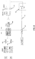
- FIG. 6 is a simplified version of the FIG. 2 topology, showing the two DPD engines 302A, 302B, the first and second post scalers 340, 350 and the VVA 360.
- the controller 304 of the DFE 112 is configured to set gain control (adjustment) values for the VVA 360 and the first and second post scalers 340, 350 based on, for example, equations below.
- Equations 6a and 6b show a mathematical form of the GC algorithm for the first PA 122, while equations 7a and 7b show the same for the second PA 124.
- first and second post scalers 340, 350 need to be modified while the common VVA can be kept constant, preserving the simplicity.
- FIG. 6 also indicates where certain terms are derived, for which see the italicised text.
- the controller 304 may operate as follows.
- Step 1 values for scaler1 and scaler2 may be calibrated to a known rated power level such that the values of error1 and error2 shown in equations 6b and 7b will be zero. Gpsi, Gps2 and Gvva are fixed during this operation.
- Step 2 with the RFM 110 powered up, RF software will compute the mean of error1 and error2.
- VVA adjustment mean error 1 + mean error 2 / 2 .
- the controller 304 accounts for the fact that one diplex path may be slightly overpowered from the target power and the other may be slightly underpowered from the target power.
- Step 2 ensures power errors of both paths will be at, or close to, a minimum. However, residual power error (over and under power from the target) is not handled. For this reason, the controller 304 requires to control the first and second post scalers 340, 350 using values of Gps 1_ adjsutment and Gps 2 _adjsutment to ensure the power of the diplex paths are now accurate.
- Step 2 indicates an embodiment where the mean error powers are computed to bring diplex path powers close to the targeted power.
- max(error1, error2) can also be used to adjust the VVA 360. This brings the path with the maximum power to the targeted power value, while the other path will be underpowered, which can be adjusted by the corresponding post scaler 340, 350.
- FIG. 7 is a flow diagram showing processing operations that may be performed, for example by the controller 304 or any one or more elements of the DFE 112 in combination.
- the controller 304 may perform at least the fourth and fifth operations relating to routing and causation of linearization.
- a first operation 701 may comprise receiving a composite signal comprising first and second predistorted input signals in first and second frequency bands.
- a third operation 703 may comprise filtering the composite signal to provide the second predistorted signal for input to a second amplifier for producing an amplified second output signal.
- a fourth operation 704 may comprise routing, at non-overlapping times, the first and second output signals to a common feedback path.
- a fifth operation 705 may comprise causing linearizing received first and second input signals based on the respective first and second output signals received on the common feedback path.
- the memory may take any suitable form.
- FIG. 9 shows a non-transitory media 1400 according to some embodiments.
- the non-transitory media 1400 is a computer readable storage medium. It may be e.g. a CD, a DVD, a USB stick, a blue ray disk, etc.
- the non-transitory media 1400 stores computer program code causing an apparatus to perform operations described above when executed by a processor such as processor 1300 of FIG 8 .
- any mentioned apparatus and/or other features of particular mentioned apparatus may be provided by apparatus arranged such that they become configured to carry out the desired operations only when enabled, e.g. switched on, or the like. In such cases, they may not necessarily have the appropriate software loaded into the active memory in the non-enabled (e.g. switched off state) and only load the appropriate software in the enabled (e.g. on state).
- the apparatus may comprise hardware circuitry and/or firmware.
- the apparatus may comprise software loaded onto memory.
- Such software/computer programs may be recorded on the same memory/processor/functional units and/or on one or more memories/processors/ functional units.
- a particular mentioned apparatus may be pre-programmed with the appropriate software to carry out desired operations, and wherein the appropriate software can be enabled for use by a user downloading a "key", for example, to unlock/enable the software and its associated functionality.
- Advantages associated with such examples can include a reduced requirement to download data when further functionality is required for a device, and this can be useful in examples where a device is perceived to have sufficient capacity to store such pre-programmed software for functionality that may not be enabled by a user.
- Any "computer” described herein can comprise a collection of one or more individual processors/processing elements that may or may not be located on the same circuit board, or the same region/position of a circuit board or even the same device. In some examples one or more of any mentioned processors may be distributed over a plurality of devices. The same or different processor/processing elements may perform one or more functions described herein.
- signal may refer to one or more signals transmitted as a series of transmitted and/or received electrical/optical signals.
- the series of signals may comprise one, two, three, four or even more individual signal components or distinct signals to make up said signalling. Some or all of these individual signals may be transmitted/received by wireless or wired communication simultaneously, in sequence, and/or such that they temporally overlap one another.
- processors and memory may comprise a computer processor, Application Specific Integrated Circuit (ASIC), field-programmable gate array (FPGA), and/or other hardware components that have been programmed in such a way to carry out the inventive function.
- ASIC Application Specific Integrated Circuit
- FPGA field-programmable gate array
Landscapes
- Engineering & Computer Science (AREA)
- Computer Networks & Wireless Communication (AREA)
- Signal Processing (AREA)
- Power Engineering (AREA)
- Microelectronics & Electronic Packaging (AREA)
- Physics & Mathematics (AREA)
- Nonlinear Science (AREA)
- Amplifiers (AREA)
Applications Claiming Priority (1)
| Application Number | Priority Date | Filing Date | Title |
|---|---|---|---|
| FI20206097 | 2020-11-02 |
Publications (1)
| Publication Number | Publication Date |
|---|---|
| EP3993262A1 true EP3993262A1 (de) | 2022-05-04 |
Family
ID=78649113
Family Applications (1)
| Application Number | Title | Priority Date | Filing Date |
|---|---|---|---|
| EP21204635.3A Pending EP3993262A1 (de) | 2020-11-02 | 2021-10-26 | Funkgerät |
Country Status (3)
| Country | Link |
|---|---|
| US (1) | US12034470B2 (de) |
| EP (1) | EP3993262A1 (de) |
| CN (1) | CN114448363B (de) |
Citations (4)
| Publication number | Priority date | Publication date | Assignee | Title |
|---|---|---|---|---|
| US20090184763A1 (en) * | 2008-01-23 | 2009-07-23 | Samsung Electronics Co. Ltd. | Apparatus and method for digital pre-distortion, sharing feedback path in a multiple antenna wireless communication system |
| US20120083229A1 (en) * | 2010-10-05 | 2012-04-05 | Peter Kenington | Radio transmitter and method for transmission of combined signal |
| CN107529215A (zh) * | 2016-06-21 | 2017-12-29 | 中兴通讯股份有限公司 | 射频发送模块的功率控制方法及射频发送模块 |
| WO2019032337A1 (en) * | 2017-08-10 | 2019-02-14 | Commscope Technologies Llc | METHODS AND APPARATUSES FOR DIGITAL PRE-DISTORTION |
Family Cites Families (24)
| Publication number | Priority date | Publication date | Assignee | Title |
|---|---|---|---|---|
| US5101173A (en) | 1990-11-28 | 1992-03-31 | The United States Of America As Represented By The Secretary Of The Air Force | Stored program controlled module amplifier bias and amplitude/phase compensation apparatus |
| US7817973B1 (en) | 2006-10-05 | 2010-10-19 | DAC Semiconductor Corporation | Method and apparatus of Doherty-type power amplifier subsystem for wireless communications systems |
| US8391812B2 (en) | 2009-08-27 | 2013-03-05 | Sige Semiconductor, Inc. | Method and system for amplifier control |
| US20110235749A1 (en) * | 2010-03-26 | 2011-09-29 | Peter Kenington | Active antenna array having analogue transmitter linearisation and a method for predistortion of radio signals |
| EP2372905B1 (de) | 2010-04-01 | 2012-06-20 | Alcatel Lucent | Doherty-Verstärkeranordnung mit verbessertem Wirkungsgrad |
| US9184710B2 (en) | 2011-02-09 | 2015-11-10 | Intel Corporation | Digital predistortion of a power amplifier for signals comprising widely spaced carriers |
| US8660207B2 (en) * | 2011-05-12 | 2014-02-25 | Andrew Llc | Digital pre-distortion with carrier cancellation |
| US9071302B2 (en) | 2011-09-06 | 2015-06-30 | Apple Inc. | Radio-frequency power amplifier circuitry with power supply voltage optimization capabilities |
| US8817859B2 (en) * | 2011-10-14 | 2014-08-26 | Fadhel Ghannouchi | Digital multi-band predistortion linearizer with nonlinear subsampling algorithm in the feedback loop |
| CN102594749A (zh) * | 2012-02-28 | 2012-07-18 | 中兴通讯股份有限公司 | 一种数字预失真处理方法及装置 |
| DE102013003903B4 (de) | 2013-03-08 | 2014-12-24 | Tesat-Spacecom Gmbh & Co.Kg | Verfahren zum Betreiben eines Verstärkermoduls eines Satelliten |
| KR101975830B1 (ko) * | 2013-04-02 | 2019-05-09 | 한국전자통신연구원 | 빔 형성 장치 및 그것의 빔 형성 방법 |
| US9385762B2 (en) | 2013-05-22 | 2016-07-05 | Telefonaktiebolaget L M Ericsson (Publ) | Linearization of intermodulation bands for concurrent dual-band power amplifiers |
| TWI554060B (zh) | 2015-03-13 | 2016-10-11 | 瑞昱半導體股份有限公司 | 傳送器以及用來降低輸入訊號失真的方法 |
| WO2016151518A1 (en) * | 2015-03-26 | 2016-09-29 | Telefonaktiebolaget Lm Ericsson (Publ) | Method and apparatus for multiband predistortion using time-shared adaptation loop |
| US9338039B1 (en) | 2015-08-26 | 2016-05-10 | Xilinx, Inc. | Efficient signal classification in digital pre-distortion systems |
| US11025203B2 (en) * | 2016-02-15 | 2021-06-01 | Solid, Inc. | Communication device and operating method thereof |
| EP3255799B1 (de) * | 2016-06-09 | 2019-07-24 | Alcatel Lucent | Verringerung von verzerrungen in verstärkten, durch ein mehrantennensystem ausgestrahlten signalen |
| WO2018126010A2 (en) * | 2016-12-29 | 2018-07-05 | Analog Devices Global | Digital predistortion for multiple power amplifiers |
| KR20190121825A (ko) | 2017-02-25 | 2019-10-28 | 나노세미, 인크. | 멀티밴드 디지털 전치왜곡기 |
| US10218318B2 (en) * | 2017-07-20 | 2019-02-26 | Arris Enterprises Llc | Amplifier with digital linearization and multiple output stages |
| GB2569121A (en) | 2017-12-05 | 2019-06-12 | Nokia Technologies Oy | Method, apparatus and arrangement for linearizing of a transmitter array |
| CN109088646B (zh) | 2018-09-06 | 2019-11-12 | 东南大学 | 针对多输入多输出发射机的共享数字预失真系统及方法 |
| KR20210108196A (ko) * | 2020-02-25 | 2021-09-02 | 주식회사 케이엠더블유 | 멀티 밴드 송신기 |
-
2021
- 2021-10-26 EP EP21204635.3A patent/EP3993262A1/de active Pending
- 2021-10-26 US US17/511,191 patent/US12034470B2/en active Active
- 2021-11-01 CN CN202111281956.XA patent/CN114448363B/zh active Active
Patent Citations (4)
| Publication number | Priority date | Publication date | Assignee | Title |
|---|---|---|---|---|
| US20090184763A1 (en) * | 2008-01-23 | 2009-07-23 | Samsung Electronics Co. Ltd. | Apparatus and method for digital pre-distortion, sharing feedback path in a multiple antenna wireless communication system |
| US20120083229A1 (en) * | 2010-10-05 | 2012-04-05 | Peter Kenington | Radio transmitter and method for transmission of combined signal |
| CN107529215A (zh) * | 2016-06-21 | 2017-12-29 | 中兴通讯股份有限公司 | 射频发送模块的功率控制方法及射频发送模块 |
| WO2019032337A1 (en) * | 2017-08-10 | 2019-02-14 | Commscope Technologies Llc | METHODS AND APPARATUSES FOR DIGITAL PRE-DISTORTION |
Also Published As
| Publication number | Publication date |
|---|---|
| CN114448363B (zh) | 2026-01-09 |
| US12034470B2 (en) | 2024-07-09 |
| CN114448363A (zh) | 2022-05-06 |
| US20220140858A1 (en) | 2022-05-05 |
Similar Documents
| Publication | Publication Date | Title |
|---|---|---|
| US9432228B2 (en) | Digital pre-distortion filter system and method | |
| US11394412B2 (en) | Predistortion circuit, method for generating a predistorted baseband signal, control circuit for a predistortion circuit, method to determine parameters for a predistortion circuit, and apparatus and method for predistorting a baseband signal | |
| US7907678B2 (en) | Power series predistorter and control method thereof | |
| EP3111554B1 (de) | Dualbandsignalübertragung | |
| US8380144B1 (en) | Systems and methods for digital predistortion in a dual band transmitter | |
| EP2754239B1 (de) | Linearisierung für einen einzelnen leistungsverstärker bei einem mehrfrequenzbandsender | |
| KR101440121B1 (ko) | 왜곡 보상 장치, 신호 송신 장치 및 그 방법 | |
| US7729668B2 (en) | Independence between paths that predistort for memory and memory-less distortion in power amplifiers | |
| US20110235749A1 (en) | Active antenna array having analogue transmitter linearisation and a method for predistortion of radio signals | |
| US20140139286A1 (en) | Systems and methods for band-limited adaptation for pa linearization | |
| US8736365B2 (en) | Broadband linearization module and method | |
| US6242978B1 (en) | Method and apparatus for linearizing an amplifier | |
| US20110235748A1 (en) | Active antenna array having analogue transmitter linearisation and a method for predistortion of radio signals | |
| US10763806B2 (en) | Envelope tracking method, system, and device employing the method | |
| US10637403B2 (en) | Digital upconversion for multi-band multi-order power amplifiers | |
| EP2779440B1 (de) | Digitale Basisband-Vorverzerrungsarchitektur | |
| CN114531168B (zh) | 无线电装置 | |
| EP0982851B1 (de) | Lineare Verstärkeranordnung | |
| US20020047746A1 (en) | Method for linearizing, over a wide frequency band a transmission chain comprising a power amplifier | |
| US12034470B2 (en) | Radio apparatus | |
| CN116982256A (zh) | 用于支持在具有数字预失真和前馈线性化的发射机系统中的互调分量抑制的方法和装置 | |
| EP2365628A1 (de) | Signalvorverarbeitung für Hüllkurvenmodulatoren | |
| KR100723541B1 (ko) | 리미터를 구비한 피드포워드 선형화 장치 | |
| KR20050077855A (ko) | 무선 통신 시스템용 전력증폭기의 채널별 송신 전력제어방법 | |
| EP2667507B1 (de) | Verstärker |
Legal Events
| Date | Code | Title | Description |
|---|---|---|---|
| PUAI | Public reference made under article 153(3) epc to a published international application that has entered the european phase |
Free format text: ORIGINAL CODE: 0009012 |
|
| STAA | Information on the status of an ep patent application or granted ep patent |
Free format text: STATUS: THE APPLICATION HAS BEEN PUBLISHED |
|
| AK | Designated contracting states |
Kind code of ref document: A1 Designated state(s): AL AT BE BG CH CY CZ DE DK EE ES FI FR GB GR HR HU IE IS IT LI LT LU LV MC MK MT NL NO PL PT RO RS SE SI SK SM TR |
|
| STAA | Information on the status of an ep patent application or granted ep patent |
Free format text: STATUS: REQUEST FOR EXAMINATION WAS MADE |
|
| 17P | Request for examination filed |
Effective date: 20221104 |
|
| RBV | Designated contracting states (corrected) |
Designated state(s): AL AT BE BG CH CY CZ DE DK EE ES FI FR GB GR HR HU IE IS IT LI LT LU LV MC MK MT NL NO PL PT RO RS SE SI SK SM TR |
|
| STAA | Information on the status of an ep patent application or granted ep patent |
Free format text: STATUS: EXAMINATION IS IN PROGRESS |
|
| 17Q | First examination report despatched |
Effective date: 20251111 |