EP3993368A1 - Module d'affichage et terminal mobile - Google Patents
Module d'affichage et terminal mobile Download PDFInfo
- Publication number
- EP3993368A1 EP3993368A1 EP20830933.6A EP20830933A EP3993368A1 EP 3993368 A1 EP3993368 A1 EP 3993368A1 EP 20830933 A EP20830933 A EP 20830933A EP 3993368 A1 EP3993368 A1 EP 3993368A1
- Authority
- EP
- European Patent Office
- Prior art keywords
- antenna array
- display module
- radio frequency
- integrated circuit
- frequency integrated
- Prior art date
- Legal status (The legal status is an assumption and is not a legal conclusion. Google has not performed a legal analysis and makes no representation as to the accuracy of the status listed.)
- Granted
Links
Images
Classifications
-
- H—ELECTRICITY
- H01—ELECTRIC ELEMENTS
- H01Q—ANTENNAS, i.e. RADIO AERIALS
- H01Q21/00—Antenna arrays or systems
- H01Q21/06—Arrays of individually energised antenna units similarly polarised and spaced apart
- H01Q21/08—Arrays of individually energised antenna units similarly polarised and spaced apart the units being spaced along or adjacent to a rectilinear path
- H01Q21/12—Parallel arrangements of substantially straight elongated conductive units
-
- H—ELECTRICITY
- H01—ELECTRIC ELEMENTS
- H01Q—ANTENNAS, i.e. RADIO AERIALS
- H01Q1/00—Details of, or arrangements associated with, antennas
- H01Q1/12—Supports; Mounting means
- H01Q1/22—Supports; Mounting means by structural association with other equipment or articles
- H01Q1/24—Supports; Mounting means by structural association with other equipment or articles with receiving set
- H01Q1/241—Supports; Mounting means by structural association with other equipment or articles with receiving set used in mobile communications, e.g. GSM
- H01Q1/242—Supports; Mounting means by structural association with other equipment or articles with receiving set used in mobile communications, e.g. GSM specially adapted for hand-held use
- H01Q1/243—Supports; Mounting means by structural association with other equipment or articles with receiving set used in mobile communications, e.g. GSM specially adapted for hand-held use with built-in antennas
-
- H—ELECTRICITY
- H01—ELECTRIC ELEMENTS
- H01Q—ANTENNAS, i.e. RADIO AERIALS
- H01Q1/00—Details of, or arrangements associated with, antennas
- H01Q1/12—Supports; Mounting means
- H01Q1/22—Supports; Mounting means by structural association with other equipment or articles
-
- G—PHYSICS
- G06—COMPUTING OR CALCULATING; COUNTING
- G06F—ELECTRIC DIGITAL DATA PROCESSING
- G06F3/00—Input arrangements for transferring data to be processed into a form capable of being handled by the computer; Output arrangements for transferring data from processing unit to output unit, e.g. interface arrangements
- G06F3/01—Input arrangements or combined input and output arrangements for interaction between user and computer
- G06F3/03—Arrangements for converting the position or the displacement of a member into a coded form
- G06F3/041—Digitisers, e.g. for touch screens or touch pads, characterised by the transducing means
- G06F3/0412—Digitisers structurally integrated in a display
-
- H—ELECTRICITY
- H01—ELECTRIC ELEMENTS
- H01Q—ANTENNAS, i.e. RADIO AERIALS
- H01Q21/00—Antenna arrays or systems
- H01Q21/06—Arrays of individually energised antenna units similarly polarised and spaced apart
- H01Q21/08—Arrays of individually energised antenna units similarly polarised and spaced apart the units being spaced along or adjacent to a rectilinear path
-
- H—ELECTRICITY
- H01—ELECTRIC ELEMENTS
- H01Q—ANTENNAS, i.e. RADIO AERIALS
- H01Q21/00—Antenna arrays or systems
- H01Q21/28—Combinations of substantially independent non-interacting antenna units or systems
-
- H—ELECTRICITY
- H01—ELECTRIC ELEMENTS
- H01Q—ANTENNAS, i.e. RADIO AERIALS
- H01Q9/00—Electrically-short antennas having dimensions not more than twice the operating wavelength and consisting of conductive active radiating elements
- H01Q9/04—Resonant antennas
- H01Q9/16—Resonant antennas with feed intermediate between the extremities of the antenna, e.g. centre-fed dipole
-
- H—ELECTRICITY
- H01—ELECTRIC ELEMENTS
- H01Q—ANTENNAS, i.e. RADIO AERIALS
- H01Q9/00—Electrically-short antennas having dimensions not more than twice the operating wavelength and consisting of conductive active radiating elements
- H01Q9/04—Resonant antennas
- H01Q9/16—Resonant antennas with feed intermediate between the extremities of the antenna, e.g. centre-fed dipole
- H01Q9/28—Conical, cylindrical, cage, strip, gauze, or like elements having an extended radiating surface; Elements comprising two conical surfaces having collinear axes and adjacent apices and fed by two-conductor transmission lines
- H01Q9/285—Planar dipole
-
- H—ELECTRICITY
- H04—ELECTRIC COMMUNICATION TECHNIQUE
- H04M—TELEPHONIC COMMUNICATION
- H04M1/00—Substation equipment, e.g. for use by subscribers
- H04M1/02—Constructional features of telephone sets
- H04M1/0202—Portable telephone sets, e.g. cordless phones, mobile phones or bar type handsets
- H04M1/026—Details of the structure or mounting of specific components
-
- H—ELECTRICITY
- H04—ELECTRIC COMMUNICATION TECHNIQUE
- H04M—TELEPHONIC COMMUNICATION
- H04M1/00—Substation equipment, e.g. for use by subscribers
- H04M1/02—Constructional features of telephone sets
- H04M1/0202—Portable telephone sets, e.g. cordless phones, mobile phones or bar type handsets
- H04M1/026—Details of the structure or mounting of specific components
- H04M1/0266—Details of the structure or mounting of specific components for a display module assembly
-
- H—ELECTRICITY
- H04—ELECTRIC COMMUNICATION TECHNIQUE
- H04M—TELEPHONIC COMMUNICATION
- H04M1/00—Substation equipment, e.g. for use by subscribers
- H04M1/02—Constructional features of telephone sets
- H04M1/0202—Portable telephone sets, e.g. cordless phones, mobile phones or bar type handsets
- H04M1/026—Details of the structure or mounting of specific components
- H04M1/0266—Details of the structure or mounting of specific components for a display module assembly
- H04M1/0268—Details of the structure or mounting of specific components for a display module assembly including a flexible display panel
-
- H—ELECTRICITY
- H04—ELECTRIC COMMUNICATION TECHNIQUE
- H04M—TELEPHONIC COMMUNICATION
- H04M1/00—Substation equipment, e.g. for use by subscribers
- H04M1/02—Constructional features of telephone sets
- H04M1/0202—Portable telephone sets, e.g. cordless phones, mobile phones or bar type handsets
- H04M1/026—Details of the structure or mounting of specific components
- H04M1/0277—Details of the structure or mounting of specific components for a printed circuit board assembly
-
- G—PHYSICS
- G06—COMPUTING OR CALCULATING; COUNTING
- G06F—ELECTRIC DIGITAL DATA PROCESSING
- G06F2203/00—Indexing scheme relating to G06F3/00 - G06F3/048
- G06F2203/041—Indexing scheme relating to G06F3/041 - G06F3/045
- G06F2203/04102—Flexible digitiser, i.e. constructional details for allowing the whole digitising part of a device to be flexed or rolled like a sheet of paper
Definitions
- the present disclosure relates to the technical field of communications equipment, and in particular, to a display module and a mobile terminal.
- phased antenna array phased antenna array
- 5G and the popular full screens of mobile phones (or other radio communications products) have increased the number of antennas, while pursuing the effect of ultimate full screen has led to continuous compression of the space for antennas.
- the current mainstream design solutions for millimeter-wave antennas primarily use the Antenna in Package (Antenna in package, AIP) technology and process, that is, to integrate the millimeter-wave array antenna, radio frequency integrated circuit (Radio Frequency Integrated Circuit, RFIC) and power management integrated module (Power Management Integrated Circuit, PMIC) into one module.
- AIP Antenna in Package
- RFIC Radio Frequency Integrated Circuit
- PMIC Power Management Integrated Circuit
- the embodiments of the present disclosure provide a display module and a mobile terminal to resolve the problem that an antenna array occupies the space for other current antennas, resulting in the degradation of antenna performance.
- an embodiment of the present disclosure provides a display module applied to a mobile terminal, the display module including a screen cover plate, a first antenna array, a first flexible circuit board, and a first radio frequency integrated circuit;
- an embodiment of the present disclosure further provides a mobile terminal, where the mobile terminal includes a display module and a carrier for carrying the display module; the display module includes a screen cover plate, a first antenna array, and a first flexible circuit board and a first radio frequency integrated circuit; where
- a first antenna array is arranged in a first region of a screen cover plate, and beam sweeping or beamforming is performed on a region above a screen by using the first antenna array.
- the antenna array designed in the embodiment of the present disclosure does not need to occupy the space for other antennas arranged on a back cover of a mobile terminal, thereby improving the performance of an antenna.
- by designing an antenna array on the glass substrate material of the screen, and multiplexing the dielectric substrate of the screen cover plate a size of the antenna can be further reduced due to the high dielectric constant of the glass substrate.
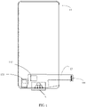
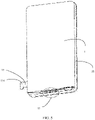
- an embodiment of the present disclosure provides a display module applied to a mobile terminal, including a screen cover plate 11, a first antenna array 12, a first flexible circuit board 13 and a first radio frequency integrated circuit 14;
- the foregoing screen cover plate is generally a glass cover plate. It is sure it may be made of other transparent non-metallic materials in the practical application.
- the foregoing first region is a region free of any metal component and only having glass medium or plastic medium, which is usually referred to as a clearance region, for example, in a mobile terminal.
- a position of the foregoing first region 111 may be set according to an actual need, and may be set at an upper or lower end of the screen cover plate 11.
- the upper and lower ends of the screen cover plate 11 are relative to the overall structure of a mobile terminal.
- a front-facing camera is set at an upper end of a mobile terminal and a microphone is set at a lower end of a mobile terminal.
- the foregoing first region 111 is located at the lower end of the screen cover plate 11.
- a width of the first region may be set according to an actual need.
- the foregoing first antenna array 12 may be set in a region with a width of less than 1mm.
- a frequency for the first antenna array 12 to receive and transmit a beam may be set according to an actual need.
- the frequency for the first antenna array 12 to receive and transmit a beam may be 60G.
- the foregoing first antenna array may be referred to as a millimeter-wave antenna array according to its wavelength.
- a connection point may be set on the first flexible circuit board 13. After the first flexible circuit board 13 is fitted with the screen cover plate 11, an electrical connection relationship between the first flexible circuit board 13 and a conductive wire on the screen cover plate 11 can be achieved based on this connection point, and an electrical connection between the first flexible circuit board 13 and the first antenna array 12 can be achieved at the same time.
- a conductive circuit is arranged on the first flexible circuit board 13, and the first radio frequency integrated circuit 14 can be electrically connected to the first antenna array 12 through the conductive circuit and the connection point.
- the first flexible circuit board 13 may be welded and fixed to the screen cover plate 11 through the connection point.
- a first antenna array 12 is arranged in a first region 111 of a screen cover plate 11, and beam sweeping or beamforming is performed on a region above the screen by using the first antenna array 12.
- the antenna array designed in the embodiment of the present disclosure does not need to occupy the space for other antennas arranged on a back cover of a mobile terminal, thereby improving the performance of an antenna.
- a size of the antenna can be further reduced due to the high dielectric constant of the glass substrate.
- the foregoing mobile terminal may include at least one of: a mobile phone, a tablet computer, an e-book reader, an MP3 player, an MP4 player, a digital camera, a laptop computer, a vehicle-mounted computer, a desktop computer, a set-top box, a smart television set, and a wearable device.
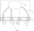
- a first connector 131 is arranged on the foregoing first flexible circuit board 13, and the first radio frequency integrated circuit 14 is electrically connected to the main board of the mobile terminal through the first connector 131.
- the foregoing first connector 131 may be a board to board (Board to Board, BTB) connector.
- the first connector 131 is configured to achieve electrical connection between the first flexible circuit board 13 and the main board, thereby ensuring the independence between the first flexible circuit board 13 and the main board while facilitating both disassembly and assembly.
- the foregoing first flexible circuit board 13 is further provided with a screen driver chip 132 and a touch detection chip 133, and the screen driver chip 132 and the touch detection chip 133 are connected to the main board through the first connector 131.
- the foregoing screen driver chip 132 may be a driver chip for a display screen to drive the display of the display screen, and the foregoing touch detection chip 133 is electrically connected to the screen cover plate 11 to detect information that the screen cover plate 11 is touched.
- the screen driver chip 132 and the touch detection chip 133 are arranged on the first flexible circuit board 13, and share the first connector 131 with the first radio frequency integrated circuit 14 to achieve a connection with the main board. For that reason, space can be saved in an effective way, which is advantageous to the miniaturization of the mobile terminal.
- the foregoing first antenna array 12 may be set according to an actual need.
- the foregoing first antenna array 12 includes at least two first dipole antenna elements 121, where the first dipole antenna element 121 includes two first dipole antennas 1211 arranged in parallel.
- a quantity of the foregoing first dipole antenna elements 121 may be set to four, where each of the first dipole antenna elements 121 includes two first dipole antennas 1211.
- the two first dipole antennas 1211 in the first dipole antenna element 121 are arranged at intervals in the length direction of the first dipole antenna 1211, and shapes and sizes of the two first dipole antennas 1211 may be consistent.
- a length of the first dipole antenna 1211 may be set to 0.55 mm
- a width may be set to 0.2 mm
- a distance between the two first dipole antennas 1211 may be 0.1 mm.
- a first bonding region (not shown in the figure) and a first feeder line 1212 corresponding to each of the first dipole antenna elements 1211 are arranged on the screen cover plate 11.
- One end of the first feeder line 1212 is electrically connected to a corresponding first dipole antenna element 1211, and the other end is electrically connected to a corresponding first bonding region, where the first bonding region is electrically connected to the first flexible circuit board 13.
- a connection point of the first flexible circuit board 13 may be electrically connected to the first bonding region through a process of thermal connection.
- the first feeder line 1212 is led out from ends (that is, opposite ends) of two opposite arms of the two first dipole antennas 1211, and extends to the first bonding region of the screen cover plate 11.
- differential feeding may be used for the two first dipole antennas 1211 of the foregoing first dipole antenna element 121, that is, amplitudes of signals from a pin of the first radio frequency integrated circuit 14 are equal, with a phase difference of 180°.
- the lengths of the two first feeder lines 1212 of the first dipole antenna element 121 are required to be the same as possible. If there is a difference, a phase of an output signal from the first radio frequency integrated circuit 14 may be compensated.
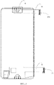
- the display module further includes a second antenna array 15, a second flexible circuit board 16, and a second radio frequency integrated circuit 17, where
- the foregoing second region 112 is located at the upper end of the screen cover plate 11, and a structure of this second region is consistent with that of the first region 111, but they are located in different positions.
- a structure of the second antenna array 15 may be consistent with that of the first antenna array 12.
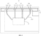
- the second antenna array 15 includes at least two second dipole antenna elements 151, and the second dipole antenna element 151 includes two second dipole antennas 1511 arranged in parallel.
- the two second dipole antennas 1511 in the second dipole antenna element 151 are arranged at intervals in the length direction of the second dipole antenna 1511, and shapes and sizes of the two second dipole antennas 1511 may be consistent.
- a length of the second dipole antenna 1511 may be set to 0.55 mm
- a width may be set to 0.2 mm
- a distance between the two second dipole antennas 1511 may be 0.1 mm.
- the second antenna array may be referred to as a millimeter-wave antenna array according to a wavelength of a beam transmitted and received by this second antenna array.
- the spatial coverage of the antenna can be improved.
- the first antenna array 12 and the second antenna array 15 may be switched for use. For example, when a user touches the first region 111, data may be transmitted and received through the second antenna array 15; when a user touches the second region 112, data may be transmitted and received through the first antenna array 12; in this way, the quality of radio communications is improved.
- a second bonding region (not shown in the figure) and a second feeder line 1512 corresponding to each of the second dipole antenna elements 1511 are arranged on the screen cover plate 11.
- One end of the second feeder line 1512 is electrically connected to a corresponding second dipole antenna element 1511, and the other end is electrically connected to a corresponding second bonding region, where the second bonding region is electrically connected to the second flexible circuit board 16.
- a connection point of the second flexible circuit board 16 may be electrically connected to the second bonding region through a process of thermal connection.
- the second feeder line 1512 is led out from ends (that is, opposite ends) of two opposite arms of the two first dipole antennas 1211, and extends to the second bonding region of the screen cover plate 11.
- differential feeding may be used for the two second dipole antennas 1511 of the foregoing second dipole antenna element 151, that is, amplitudes of signals from a pin of the second radio frequency integrated circuit 17 are equal, with a phase difference of 180°.
- the lengths of the two second feeder lines 1512 of the second dipole antenna element 151 are required to be the same as possible. If there is a difference, a phase of an output signal from the second radio frequency integrated circuit 17 may be compensated.
- a second connector 161 is arranged on the foregoing second flexible circuit board 16, and the second radio frequency integrated circuit 17 is electrically connected to the main board of the mobile terminal through the second connector 161.
- the foregoing second connector 161 may be a board to board (Board to Board, BTB) connector.
- the second connector 161 is configured to achieve electrical connection between the second flexible circuit board 16 and the main board, thereby ensuring the independence between the second flexible circuit board 16 and the main board while facilitating both disassembly and assembly.
- an embodiment of the present disclosure further provides a mobile terminal.
- the mobile terminal includes a display module and a carrier 18 carrying the display module.
- the carrier 18 may be a front case or a middle frame.
- the foregoing display module is the display module in the foregoing embodiment.
- a mobile terminal provided in this embodiment has all beneficial effects of the display module in the foregoing embodiment.
- the carrier 18 is a metal carrier, and the metal carrier is used as a reflector for the antenna array of the display module.
- This spacing may be understood as a vertical distance from each first dipole antenna element 121 in the first antenna array 12 to the carrier 18 in the thickness direction of the mobile terminal, and a vertical distance from each second dipole antenna element 151 in the second antenna array 15 to the carrier 18 in the thickness direction of the mobile terminal, and a size of such spacing may be set according to an actual need.
- the foregoing carrier 18 may be made of metal material at a position corresponding to the first antenna array 12 and the second antenna array 15 in the thickness direction, or may be made of metal material as a whole, which is not further limited herein.
- the carrier 18 is a metal carrier, it may act as a reflector for the antenna array, which can make the maximum radiation direction of the antenna array face the side of the screen, thereby increasing the gain of the first antenna array 12 and the second antenna array 15, and enhancing the radio communications quality.
- the vertical distance from each first dipole antenna element 121 to the carrier 18 is set to 0.37 mm, and the vertical distance from each second dipole antenna element 151 to the carrier 18 is set to 0.37 mm. In this way, the beam for 60G frequency can improve the communications quality to the greatest extent.
- the display module includes a first antenna array 12, a first radio frequency integrated circuit 14, a second antenna array 15 and a second radio frequency integrated circuit 17,
- the foregoing control chip may be set on the main board and configured to control work states of the first radio frequency integrated circuit 14 and the second radio frequency integrated circuit 17. Additionally, the control chip may further be electrically connected to a touch detection chip 133, and determine touch states of the first region 111 and the second region 112 according to a user's touch position detected by the touch detection chip 133, and thus control the work states of the first radio frequency integrated circuit 14 and the second radio frequency integrated circuit 17.
Landscapes
- Engineering & Computer Science (AREA)
- Signal Processing (AREA)
- Computer Networks & Wireless Communication (AREA)
- General Engineering & Computer Science (AREA)
- Theoretical Computer Science (AREA)
- Human Computer Interaction (AREA)
- Physics & Mathematics (AREA)
- General Physics & Mathematics (AREA)
- Variable-Direction Aerials And Aerial Arrays (AREA)
- Telephone Set Structure (AREA)
- Support Of Aerials (AREA)
- Details Of Aerials (AREA)
Applications Claiming Priority (2)
| Application Number | Priority Date | Filing Date | Title |
|---|---|---|---|
| CN201910562658.4A CN110312009B (zh) | 2019-06-26 | 2019-06-26 | 一种显示模组及移动终端 |
| PCT/CN2020/095548 WO2020259300A1 (fr) | 2019-06-26 | 2020-06-11 | Module d'affichage et terminal mobile |
Publications (3)
| Publication Number | Publication Date |
|---|---|
| EP3993368A1 true EP3993368A1 (fr) | 2022-05-04 |
| EP3993368A4 EP3993368A4 (fr) | 2022-08-10 |
| EP3993368B1 EP3993368B1 (fr) | 2023-10-25 |
Family
ID=68077595
Family Applications (1)
| Application Number | Title | Priority Date | Filing Date |
|---|---|---|---|
| EP20830933.6A Active EP3993368B1 (fr) | 2019-06-26 | 2020-06-11 | Module d'affichage et terminal mobile |
Country Status (7)
| Country | Link |
|---|---|
| US (1) | US12218406B2 (fr) |
| EP (1) | EP3993368B1 (fr) |
| JP (1) | JP7345571B2 (fr) |
| KR (1) | KR102582482B1 (fr) |
| CN (1) | CN110312009B (fr) |
| ES (1) | ES2965166T3 (fr) |
| WO (1) | WO2020259300A1 (fr) |
Families Citing this family (12)
| Publication number | Priority date | Publication date | Assignee | Title |
|---|---|---|---|---|
| CN112740478B (zh) * | 2019-03-04 | 2022-02-25 | 华为技术有限公司 | 毫米波组件 |
| CN110312009B (zh) | 2019-06-26 | 2021-03-02 | 维沃移动通信有限公司 | 一种显示模组及移动终端 |
| CN111276063B (zh) * | 2020-02-26 | 2022-04-26 | 维沃移动通信有限公司 | 一种显示模组及电子设备 |
| CN114122678A (zh) * | 2020-08-25 | 2022-03-01 | 深圳市万普拉斯科技有限公司 | 一种电子设备 |
| CN112054282A (zh) * | 2020-08-31 | 2020-12-08 | 瑞声新能源发展(常州)有限公司科教城分公司 | 天线结构及移动终端 |
| CN112054281A (zh) * | 2020-08-31 | 2020-12-08 | 瑞声新能源发展(常州)有限公司科教城分公司 | 天线结构及移动终端 |
| CN112448129A (zh) * | 2020-12-08 | 2021-03-05 | 维沃移动通信有限公司 | 一种显示模组及电子设备 |
| USD1059361S1 (en) * | 2020-12-11 | 2025-01-28 | Samsung Display Co., Ltd. | Display module |
| CN112929475B (zh) * | 2021-02-04 | 2023-12-08 | 维沃移动通信有限公司 | 电子设备 |
| CN116093636B (zh) * | 2022-01-12 | 2024-04-12 | 荣耀终端有限公司 | 毫米波模组电路及终端设备 |
| US20240097318A1 (en) * | 2022-05-16 | 2024-03-21 | Meta Platforms Technologies, Llc | Transparent antenna and touch display on a wearable device |
| CN116706580A (zh) * | 2023-08-03 | 2023-09-05 | 合肥国家实验室 | 基于fpc的多通道射频连接器 |
Family Cites Families (27)
| Publication number | Priority date | Publication date | Assignee | Title |
|---|---|---|---|---|
| JP2003110329A (ja) | 2001-07-25 | 2003-04-11 | Matsushita Electric Ind Co Ltd | 内蔵アンテナ装置 |
| WO2009029520A1 (fr) | 2007-08-27 | 2009-03-05 | Rambus Inc. | Antenne-réseau à interconnexion souple pour un dispositif mobile sans fil |
| KR101004405B1 (ko) * | 2008-08-20 | 2010-12-28 | 이미지랩(주) | 터치 패널 |
| US8686902B2 (en) * | 2009-05-13 | 2014-04-01 | Norberto Lopez | Antenna structures |
| US9268420B2 (en) | 2012-03-05 | 2016-02-23 | Htc Corporation | Touch panel structure and touch display panel structure having antenna pattern and related communications device having such touch panel structure |
| CN102882545B (zh) * | 2012-09-21 | 2015-08-05 | 敦泰科技有限公司 | 一种通信设备 |
| JP6437285B2 (ja) | 2014-11-21 | 2018-12-12 | シャープ株式会社 | 通信装置、および通信装置の制御方法 |
| CN106708298B (zh) * | 2015-07-17 | 2023-09-22 | 宸鸿科技(厦门)有限公司 | 触控面板及其接合结构 |
| US10418687B2 (en) * | 2016-07-22 | 2019-09-17 | Apple Inc. | Electronic device with millimeter wave antennas on printed circuits |
| CN106229626A (zh) | 2016-09-12 | 2016-12-14 | 深圳市金诺和信通讯有限公司 | 具有天线功能的透明面板、显示屏组件及无线通信设备 |
| CN206452415U (zh) * | 2017-01-10 | 2017-08-29 | 广东欧珀移动通信有限公司 | 移动终端 |
| KR102562001B1 (ko) * | 2017-01-13 | 2023-08-02 | 삼성전자주식회사 | 발광 장치를 포함하는 전자 장치 |
| CN206628591U (zh) * | 2017-03-24 | 2017-11-10 | 维沃移动通信有限公司 | 一种天线结构及移动终端 |
| CN106876881B (zh) * | 2017-03-27 | 2020-06-23 | 联想(北京)有限公司 | 移动终端 |
| KR102348241B1 (ko) * | 2017-05-30 | 2022-01-10 | 삼성전자주식회사 | 안테나 어레이 및 안테나 어레이를 포함하는 전자 장치 |
| US10476136B2 (en) * | 2017-07-20 | 2019-11-12 | Apple Inc. | Electronic device with speaker port aligned antennas |
| US11605883B2 (en) * | 2017-07-28 | 2023-03-14 | Samsung Electro-Mechanics Co., Ltd. | Antenna module including a flexible substrate |
| US10381750B2 (en) * | 2017-08-17 | 2019-08-13 | Lg Electronics Inc. | Electronic device |
| KR102439813B1 (ko) * | 2017-09-29 | 2022-09-02 | 엘지전자 주식회사 | 이동 단말기 |
| US10455065B2 (en) * | 2017-09-29 | 2019-10-22 | Lg Electronics Inc. | Mobile terminal |
| US10775490B2 (en) * | 2017-10-12 | 2020-09-15 | Infineon Technologies Ag | Radio frequency systems integrated with displays and methods of formation thereof |
| CN108521499B (zh) * | 2018-03-12 | 2020-11-13 | Oppo广东移动通信有限公司 | 天线切换方法、存储介质及电子设备 |
| CN108881527A (zh) * | 2018-05-23 | 2018-11-23 | 深圳市海德门电子有限公司 | 屏幕、设备、屏幕的制备方法 |
| KR102162228B1 (ko) * | 2018-07-05 | 2020-10-06 | 동우 화인켐 주식회사 | 안테나 구조체 및 이를 포함하는 디스플레이 장치 |
| CN110312009B (zh) * | 2019-06-26 | 2021-03-02 | 维沃移动通信有限公司 | 一种显示模组及移动终端 |
| US12451938B2 (en) * | 2020-03-05 | 2025-10-21 | Lg Electronics Inc. | Electronic device comprising antenna |
| KR20240129701A (ko) * | 2023-02-21 | 2024-08-28 | 동우 화인켐 주식회사 | 안테나 구조체 및 이를 포함하는 화상 표시 장치 |
-
2019
- 2019-06-26 CN CN201910562658.4A patent/CN110312009B/zh active Active
-
2020
- 2020-06-11 JP JP2021574993A patent/JP7345571B2/ja active Active
- 2020-06-11 KR KR1020217041499A patent/KR102582482B1/ko active Active
- 2020-06-11 EP EP20830933.6A patent/EP3993368B1/fr active Active
- 2020-06-11 WO PCT/CN2020/095548 patent/WO2020259300A1/fr not_active Ceased
- 2020-06-11 ES ES20830933T patent/ES2965166T3/es active Active
-
2021
- 2021-12-15 US US17/552,096 patent/US12218406B2/en active Active
Also Published As
| Publication number | Publication date |
|---|---|
| US20220109225A1 (en) | 2022-04-07 |
| EP3993368A4 (fr) | 2022-08-10 |
| EP3993368B1 (fr) | 2023-10-25 |
| US12218406B2 (en) | 2025-02-04 |
| WO2020259300A1 (fr) | 2020-12-30 |
| JP7345571B2 (ja) | 2023-09-15 |
| KR20220008348A (ko) | 2022-01-20 |
| JP2022537307A (ja) | 2022-08-25 |
| ES2965166T3 (es) | 2024-04-11 |
| CN110312009A (zh) | 2019-10-08 |
| KR102582482B1 (ko) | 2023-09-22 |
| CN110312009B (zh) | 2021-03-02 |
Similar Documents
| Publication | Publication Date | Title |
|---|---|---|
| US12218406B2 (en) | Display module and mobile terminal | |
| AU2021205050B2 (en) | Dual polarized antenna and electronic device including the same | |
| US11145993B2 (en) | Antenna module and terminal thereof | |
| CN112768904B (zh) | 天线辐射体、天线组件及电子设备 | |
| US12015192B2 (en) | Terminal device | |
| US12519217B2 (en) | Display apparatus and electronic device | |
| CN105655701B (zh) | 天线装置和移动终端 | |
| EP3920322B1 (fr) | Appareil d'antenne et dispositif électronique | |
| US20200144722A1 (en) | Antenna and electronic device including dielectric overlapped with at least portion of the antenna | |
| CN110867662A (zh) | 天线封装模组和电子设备 | |
| CN110854507A (zh) | 天线封装模组和电子设备 | |
| KR20150014152A (ko) | 무선 통신 장치 | |
| CN107331947A (zh) | 一种移动终端用缝隙天线以及移动终端 | |
| CN111276063B (zh) | 一种显示模组及电子设备 | |
| JP2017034652A (ja) | 移動端末 | |
| CN117882247A (zh) | 天线以及包括天线的电子装置 | |
| CN109728414A (zh) | 一种天线结构及终端设备 | |
| US9059500B2 (en) | Capacitive loop antenna and electronic device | |
| CN112333307A (zh) | 显示组件和电子设备 | |
| TWI734061B (zh) | 多天線系統及其電子裝置 | |
| CN112965634B (zh) | 显示模组和电子设备 | |
| CN115579633A (zh) | 天线及具有该天线的无线通信装置 | |
| KR20240070354A (ko) | 안테나 모듈 및 상기 안테나 모듈을 포함하는 전자 장치 | |
| WO2024103947A1 (fr) | Ensemble décoratif pour caméra, module de caméra et dispositif électronique | |
| CN102142615A (zh) | 天线模块 |
Legal Events
| Date | Code | Title | Description |
|---|---|---|---|
| STAA | Information on the status of an ep patent application or granted ep patent |
Free format text: STATUS: THE INTERNATIONAL PUBLICATION HAS BEEN MADE |
|
| PUAI | Public reference made under article 153(3) epc to a published international application that has entered the european phase |
Free format text: ORIGINAL CODE: 0009012 |
|
| STAA | Information on the status of an ep patent application or granted ep patent |
Free format text: STATUS: REQUEST FOR EXAMINATION WAS MADE |
|
| 17P | Request for examination filed |
Effective date: 20211215 |
|
| AK | Designated contracting states |
Kind code of ref document: A1 Designated state(s): AL AT BE BG CH CY CZ DE DK EE ES FI FR GB GR HR HU IE IS IT LI LT LU LV MC MK MT NL NO PL PT RO RS SE SI SK SM TR |
|
| A4 | Supplementary search report drawn up and despatched |
Effective date: 20220711 |
|
| RIC1 | Information provided on ipc code assigned before grant |
Ipc: H04B 7/06 20060101ALI20220705BHEP Ipc: H01Q 1/24 20060101ALI20220705BHEP Ipc: H04M 1/02 20060101AFI20220705BHEP |
|
| DAV | Request for validation of the european patent (deleted) | ||
| DAX | Request for extension of the european patent (deleted) | ||
| GRAP | Despatch of communication of intention to grant a patent |
Free format text: ORIGINAL CODE: EPIDOSNIGR1 |
|
| STAA | Information on the status of an ep patent application or granted ep patent |
Free format text: STATUS: GRANT OF PATENT IS INTENDED |
|
| INTG | Intention to grant announced |
Effective date: 20230524 |
|
| GRAS | Grant fee paid |
Free format text: ORIGINAL CODE: EPIDOSNIGR3 |
|
| GRAA | (expected) grant |
Free format text: ORIGINAL CODE: 0009210 |
|
| STAA | Information on the status of an ep patent application or granted ep patent |
Free format text: STATUS: THE PATENT HAS BEEN GRANTED |
|
| AK | Designated contracting states |
Kind code of ref document: B1 Designated state(s): AL AT BE BG CH CY CZ DE DK EE ES FI FR GB GR HR HU IE IS IT LI LT LU LV MC MK MT NL NO PL PT RO RS SE SI SK SM TR |
|
| REG | Reference to a national code |
Ref country code: GB Ref legal event code: FG4D |
|
| REG | Reference to a national code |
Ref country code: CH Ref legal event code: EP |
|
| REG | Reference to a national code |
Ref country code: DE Ref legal event code: R096 Ref document number: 602020019982 Country of ref document: DE |
|
| REG | Reference to a national code |
Ref country code: IE Ref legal event code: FG4D |
|
| REG | Reference to a national code |
Ref country code: NL Ref legal event code: FP |
|
| REG | Reference to a national code |
Ref country code: LT Ref legal event code: MG9D |
|
| REG | Reference to a national code |
Ref country code: AT Ref legal event code: MK05 Ref document number: 1625865 Country of ref document: AT Kind code of ref document: T Effective date: 20231025 |
|
| PG25 | Lapsed in a contracting state [announced via postgrant information from national office to epo] |
Ref country code: GR Free format text: LAPSE BECAUSE OF FAILURE TO SUBMIT A TRANSLATION OF THE DESCRIPTION OR TO PAY THE FEE WITHIN THE PRESCRIBED TIME-LIMIT Effective date: 20240126 |
|
| PG25 | Lapsed in a contracting state [announced via postgrant information from national office to epo] |
Ref country code: IS Free format text: LAPSE BECAUSE OF FAILURE TO SUBMIT A TRANSLATION OF THE DESCRIPTION OR TO PAY THE FEE WITHIN THE PRESCRIBED TIME-LIMIT Effective date: 20240225 |
|
| REG | Reference to a national code |
Ref country code: ES Ref legal event code: FG2A Ref document number: 2965166 Country of ref document: ES Kind code of ref document: T3 Effective date: 20240411 |
|
| PG25 | Lapsed in a contracting state [announced via postgrant information from national office to epo] |
Ref country code: LT Free format text: LAPSE BECAUSE OF FAILURE TO SUBMIT A TRANSLATION OF THE DESCRIPTION OR TO PAY THE FEE WITHIN THE PRESCRIBED TIME-LIMIT Effective date: 20231025 |
|
| PG25 | Lapsed in a contracting state [announced via postgrant information from national office to epo] |
Ref country code: AT Free format text: LAPSE BECAUSE OF FAILURE TO SUBMIT A TRANSLATION OF THE DESCRIPTION OR TO PAY THE FEE WITHIN THE PRESCRIBED TIME-LIMIT Effective date: 20231025 |
|
| PG25 | Lapsed in a contracting state [announced via postgrant information from national office to epo] |
Ref country code: LT Free format text: LAPSE BECAUSE OF FAILURE TO SUBMIT A TRANSLATION OF THE DESCRIPTION OR TO PAY THE FEE WITHIN THE PRESCRIBED TIME-LIMIT Effective date: 20231025 Ref country code: IS Free format text: LAPSE BECAUSE OF FAILURE TO SUBMIT A TRANSLATION OF THE DESCRIPTION OR TO PAY THE FEE WITHIN THE PRESCRIBED TIME-LIMIT Effective date: 20240225 Ref country code: GR Free format text: LAPSE BECAUSE OF FAILURE TO SUBMIT A TRANSLATION OF THE DESCRIPTION OR TO PAY THE FEE WITHIN THE PRESCRIBED TIME-LIMIT Effective date: 20240126 Ref country code: BG Free format text: LAPSE BECAUSE OF FAILURE TO SUBMIT A TRANSLATION OF THE DESCRIPTION OR TO PAY THE FEE WITHIN THE PRESCRIBED TIME-LIMIT Effective date: 20240125 Ref country code: AT Free format text: LAPSE BECAUSE OF FAILURE TO SUBMIT A TRANSLATION OF THE DESCRIPTION OR TO PAY THE FEE WITHIN THE PRESCRIBED TIME-LIMIT Effective date: 20231025 Ref country code: PT Free format text: LAPSE BECAUSE OF FAILURE TO SUBMIT A TRANSLATION OF THE DESCRIPTION OR TO PAY THE FEE WITHIN THE PRESCRIBED TIME-LIMIT Effective date: 20240226 |
|
| PG25 | Lapsed in a contracting state [announced via postgrant information from national office to epo] |
Ref country code: SE Free format text: LAPSE BECAUSE OF FAILURE TO SUBMIT A TRANSLATION OF THE DESCRIPTION OR TO PAY THE FEE WITHIN THE PRESCRIBED TIME-LIMIT Effective date: 20231025 Ref country code: RS Free format text: LAPSE BECAUSE OF FAILURE TO SUBMIT A TRANSLATION OF THE DESCRIPTION OR TO PAY THE FEE WITHIN THE PRESCRIBED TIME-LIMIT Effective date: 20231025 Ref country code: PL Free format text: LAPSE BECAUSE OF FAILURE TO SUBMIT A TRANSLATION OF THE DESCRIPTION OR TO PAY THE FEE WITHIN THE PRESCRIBED TIME-LIMIT Effective date: 20231025 Ref country code: NO Free format text: LAPSE BECAUSE OF FAILURE TO SUBMIT A TRANSLATION OF THE DESCRIPTION OR TO PAY THE FEE WITHIN THE PRESCRIBED TIME-LIMIT Effective date: 20240125 Ref country code: LV Free format text: LAPSE BECAUSE OF FAILURE TO SUBMIT A TRANSLATION OF THE DESCRIPTION OR TO PAY THE FEE WITHIN THE PRESCRIBED TIME-LIMIT Effective date: 20231025 Ref country code: HR Free format text: LAPSE BECAUSE OF FAILURE TO SUBMIT A TRANSLATION OF THE DESCRIPTION OR TO PAY THE FEE WITHIN THE PRESCRIBED TIME-LIMIT Effective date: 20231025 |
|
| PG25 | Lapsed in a contracting state [announced via postgrant information from national office to epo] |
Ref country code: DK Free format text: LAPSE BECAUSE OF FAILURE TO SUBMIT A TRANSLATION OF THE DESCRIPTION OR TO PAY THE FEE WITHIN THE PRESCRIBED TIME-LIMIT Effective date: 20231025 |
|
| PG25 | Lapsed in a contracting state [announced via postgrant information from national office to epo] |
Ref country code: CZ Free format text: LAPSE BECAUSE OF FAILURE TO SUBMIT A TRANSLATION OF THE DESCRIPTION OR TO PAY THE FEE WITHIN THE PRESCRIBED TIME-LIMIT Effective date: 20231025 |
|
| REG | Reference to a national code |
Ref country code: DE Ref legal event code: R097 Ref document number: 602020019982 Country of ref document: DE |
|
| PG25 | Lapsed in a contracting state [announced via postgrant information from national office to epo] |
Ref country code: SK Free format text: LAPSE BECAUSE OF FAILURE TO SUBMIT A TRANSLATION OF THE DESCRIPTION OR TO PAY THE FEE WITHIN THE PRESCRIBED TIME-LIMIT Effective date: 20231025 |
|
| PG25 | Lapsed in a contracting state [announced via postgrant information from national office to epo] |
Ref country code: SM Free format text: LAPSE BECAUSE OF FAILURE TO SUBMIT A TRANSLATION OF THE DESCRIPTION OR TO PAY THE FEE WITHIN THE PRESCRIBED TIME-LIMIT Effective date: 20231025 Ref country code: SK Free format text: LAPSE BECAUSE OF FAILURE TO SUBMIT A TRANSLATION OF THE DESCRIPTION OR TO PAY THE FEE WITHIN THE PRESCRIBED TIME-LIMIT Effective date: 20231025 Ref country code: RO Free format text: LAPSE BECAUSE OF FAILURE TO SUBMIT A TRANSLATION OF THE DESCRIPTION OR TO PAY THE FEE WITHIN THE PRESCRIBED TIME-LIMIT Effective date: 20231025 Ref country code: EE Free format text: LAPSE BECAUSE OF FAILURE TO SUBMIT A TRANSLATION OF THE DESCRIPTION OR TO PAY THE FEE WITHIN THE PRESCRIBED TIME-LIMIT Effective date: 20231025 Ref country code: DK Free format text: LAPSE BECAUSE OF FAILURE TO SUBMIT A TRANSLATION OF THE DESCRIPTION OR TO PAY THE FEE WITHIN THE PRESCRIBED TIME-LIMIT Effective date: 20231025 Ref country code: CZ Free format text: LAPSE BECAUSE OF FAILURE TO SUBMIT A TRANSLATION OF THE DESCRIPTION OR TO PAY THE FEE WITHIN THE PRESCRIBED TIME-LIMIT Effective date: 20231025 |
|
| PLBE | No opposition filed within time limit |
Free format text: ORIGINAL CODE: 0009261 |
|
| STAA | Information on the status of an ep patent application or granted ep patent |
Free format text: STATUS: NO OPPOSITION FILED WITHIN TIME LIMIT |
|
| 26N | No opposition filed |
Effective date: 20240726 |
|
| PG25 | Lapsed in a contracting state [announced via postgrant information from national office to epo] |
Ref country code: SI Free format text: LAPSE BECAUSE OF FAILURE TO SUBMIT A TRANSLATION OF THE DESCRIPTION OR TO PAY THE FEE WITHIN THE PRESCRIBED TIME-LIMIT Effective date: 20231025 |
|
| PG25 | Lapsed in a contracting state [announced via postgrant information from national office to epo] |
Ref country code: SI Free format text: LAPSE BECAUSE OF FAILURE TO SUBMIT A TRANSLATION OF THE DESCRIPTION OR TO PAY THE FEE WITHIN THE PRESCRIBED TIME-LIMIT Effective date: 20231025 |
|
| PG25 | Lapsed in a contracting state [announced via postgrant information from national office to epo] |
Ref country code: MC Free format text: LAPSE BECAUSE OF FAILURE TO SUBMIT A TRANSLATION OF THE DESCRIPTION OR TO PAY THE FEE WITHIN THE PRESCRIBED TIME-LIMIT Effective date: 20231025 |
|
| REG | Reference to a national code |
Ref country code: CH Ref legal event code: PL |
|
| PG25 | Lapsed in a contracting state [announced via postgrant information from national office to epo] |
Ref country code: LU Free format text: LAPSE BECAUSE OF NON-PAYMENT OF DUE FEES Effective date: 20240611 |
|
| PG25 | Lapsed in a contracting state [announced via postgrant information from national office to epo] |
Ref country code: IE Free format text: LAPSE BECAUSE OF NON-PAYMENT OF DUE FEES Effective date: 20240611 |
|
| PG25 | Lapsed in a contracting state [announced via postgrant information from national office to epo] |
Ref country code: BE Free format text: LAPSE BECAUSE OF NON-PAYMENT OF DUE FEES Effective date: 20240630 Ref country code: CH Free format text: LAPSE BECAUSE OF NON-PAYMENT OF DUE FEES Effective date: 20240630 |
|
| REG | Reference to a national code |
Ref country code: BE Ref legal event code: MM Effective date: 20240630 |
|
| PGFP | Annual fee paid to national office [announced via postgrant information from national office to epo] |
Ref country code: NL Payment date: 20250516 Year of fee payment: 6 |
|
| PGFP | Annual fee paid to national office [announced via postgrant information from national office to epo] |
Ref country code: DE Payment date: 20250429 Year of fee payment: 6 |
|
| PGFP | Annual fee paid to national office [announced via postgrant information from national office to epo] |
Ref country code: GB Payment date: 20250501 Year of fee payment: 6 |
|
| PGFP | Annual fee paid to national office [announced via postgrant information from national office to epo] |
Ref country code: IT Payment date: 20250522 Year of fee payment: 6 |
|
| PGFP | Annual fee paid to national office [announced via postgrant information from national office to epo] |
Ref country code: FR Payment date: 20250508 Year of fee payment: 6 |
|
| PG25 | Lapsed in a contracting state [announced via postgrant information from national office to epo] |
Ref country code: FI Free format text: LAPSE BECAUSE OF FAILURE TO SUBMIT A TRANSLATION OF THE DESCRIPTION OR TO PAY THE FEE WITHIN THE PRESCRIBED TIME-LIMIT Effective date: 20231025 |
|
| PGFP | Annual fee paid to national office [announced via postgrant information from national office to epo] |
Ref country code: ES Payment date: 20250703 Year of fee payment: 6 |
|
| PG25 | Lapsed in a contracting state [announced via postgrant information from national office to epo] |
Ref country code: CY Free format text: LAPSE BECAUSE OF FAILURE TO SUBMIT A TRANSLATION OF THE DESCRIPTION OR TO PAY THE FEE WITHIN THE PRESCRIBED TIME-LIMIT; INVALID AB INITIO Effective date: 20200611 |
|
| PG25 | Lapsed in a contracting state [announced via postgrant information from national office to epo] |
Ref country code: HU Free format text: LAPSE BECAUSE OF FAILURE TO SUBMIT A TRANSLATION OF THE DESCRIPTION OR TO PAY THE FEE WITHIN THE PRESCRIBED TIME-LIMIT; INVALID AB INITIO Effective date: 20200611 |