EP3993441A1 - Filtre miniature et dispositif acoustique - Google Patents
Filtre miniature et dispositif acoustique Download PDFInfo
- Publication number
- EP3993441A1 EP3993441A1 EP19935734.4A EP19935734A EP3993441A1 EP 3993441 A1 EP3993441 A1 EP 3993441A1 EP 19935734 A EP19935734 A EP 19935734A EP 3993441 A1 EP3993441 A1 EP 3993441A1
- Authority
- EP
- European Patent Office
- Prior art keywords
- filter
- micro
- film layer
- diaphragm
- substrate
- Prior art date
- Legal status (The legal status is an assumption and is not a legal conclusion. Google has not performed a legal analysis and makes no representation as to the accuracy of the status listed.)
- Granted
Links
Images


Classifications
-
- H—ELECTRICITY
- H04—ELECTRIC COMMUNICATION TECHNIQUE
- H04R—LOUDSPEAKERS, MICROPHONES, GRAMOPHONE PICK-UPS OR LIKE ACOUSTIC ELECTROMECHANICAL TRANSDUCERS; ELECTRIC HEARING AIDS; PUBLIC ADDRESS SYSTEMS
- H04R1/00—Details of transducers, loudspeakers or microphones
- H04R1/02—Casings; Cabinets ; Supports therefor; Mountings therein
- H04R1/023—Screens for loudspeakers
-
- B—PERFORMING OPERATIONS; TRANSPORTING
- B01—PHYSICAL OR CHEMICAL PROCESSES OR APPARATUS IN GENERAL
- B01D—SEPARATION
- B01D46/00—Filters or filtering processes specially modified for separating dispersed particles from gases or vapours
- B01D46/54—Particle separators, e.g. dust precipitators, using ultra-fine filter sheets or diaphragms
- B01D46/543—Particle separators, e.g. dust precipitators, using ultra-fine filter sheets or diaphragms using membranes
-
- H—ELECTRICITY
- H04—ELECTRIC COMMUNICATION TECHNIQUE
- H04R—LOUDSPEAKERS, MICROPHONES, GRAMOPHONE PICK-UPS OR LIKE ACOUSTIC ELECTROMECHANICAL TRANSDUCERS; ELECTRIC HEARING AIDS; PUBLIC ADDRESS SYSTEMS
- H04R1/00—Details of transducers, loudspeakers or microphones
- H04R1/08—Mouthpieces; Microphones; Attachments therefor
- H04R1/083—Special constructions of mouthpieces
- H04R1/086—Protective screens, e.g. all weather or wind screens
-
- H—ELECTRICITY
- H04—ELECTRIC COMMUNICATION TECHNIQUE
- H04R—LOUDSPEAKERS, MICROPHONES, GRAMOPHONE PICK-UPS OR LIKE ACOUSTIC ELECTROMECHANICAL TRANSDUCERS; ELECTRIC HEARING AIDS; PUBLIC ADDRESS SYSTEMS
- H04R7/00—Diaphragms for electromechanical transducers; Cones
- H04R7/02—Diaphragms for electromechanical transducers; Cones characterised by the construction
- H04R7/12—Non-planar diaphragms or cones
-
- H—ELECTRICITY
- H04—ELECTRIC COMMUNICATION TECHNIQUE
- H04R—LOUDSPEAKERS, MICROPHONES, GRAMOPHONE PICK-UPS OR LIKE ACOUSTIC ELECTROMECHANICAL TRANSDUCERS; ELECTRIC HEARING AIDS; PUBLIC ADDRESS SYSTEMS
- H04R9/00—Transducers of moving-coil, moving-strip, or moving-wire type
- H04R9/02—Details
-
- H—ELECTRICITY
- H04—ELECTRIC COMMUNICATION TECHNIQUE
- H04R—LOUDSPEAKERS, MICROPHONES, GRAMOPHONE PICK-UPS OR LIKE ACOUSTIC ELECTROMECHANICAL TRANSDUCERS; ELECTRIC HEARING AIDS; PUBLIC ADDRESS SYSTEMS
- H04R9/00—Transducers of moving-coil, moving-strip, or moving-wire type
- H04R9/06—Loudspeakers
-
- H—ELECTRICITY
- H04—ELECTRIC COMMUNICATION TECHNIQUE
- H04R—LOUDSPEAKERS, MICROPHONES, GRAMOPHONE PICK-UPS OR LIKE ACOUSTIC ELECTROMECHANICAL TRANSDUCERS; ELECTRIC HEARING AIDS; PUBLIC ADDRESS SYSTEMS
- H04R2207/00—Details of diaphragms or cones for electromechanical transducers or their suspension covered by H04R7/00 but not provided for in H04R7/00 or in H04R2307/00
- H04R2207/021—Diaphragm extensions, not necessarily integrally formed, e.g. skirts, rims, flanges
-
- H—ELECTRICITY
- H04—ELECTRIC COMMUNICATION TECHNIQUE
- H04R—LOUDSPEAKERS, MICROPHONES, GRAMOPHONE PICK-UPS OR LIKE ACOUSTIC ELECTROMECHANICAL TRANSDUCERS; ELECTRIC HEARING AIDS; PUBLIC ADDRESS SYSTEMS
- H04R2400/00—Loudspeakers
- H04R2400/11—Aspects regarding the frame of loudspeaker transducers
Definitions
- the present disclosure relates to a micro-filter, which may be a micro-filter suitable for an acoustic device so as to filter substances such as dust, particles or/and water that are not desired to enter into the interior of the acoustic device.
- Portable computing devices such as laptops and tablets are ubiquitous, and so are portable communication devices such as smart phones.
- portable communication devices such as smart phones.
- microphones and speakers are decreasing in size and are becoming more and more compact.
- microphones and speakers in such portable devices often need to be close to relevant acoustic input or output ports of a terminal, and thus tend to cause failure of these acoustic devices due to particle or water ingress of the microphones and speakers.
- a filter film was sometimes deployed in a prior art device to prevent certain types of debris from entering components thereof.
- Such filters tend to adversely affect operation of the microphone.
- performance of a microphone is sometimes significantly degraded when such prior art methods are used.
- Customers of the microphone often choose not to use such microphones in their applications due to the degraded performance.
- Ordinary metal films have stress limits when making a filter film. When an ordinary metal film is under stress and exhibits compression that forms a corrugation, the pressure cannot be detected with an optical automatic detection device.
- a film with low tensile stress is required when depositing a suitable thin metal film onto the substrate. A film without low tensile stress tend to peel, crack, crepe or otherwise detach from its substrate, inevitably resulting in frequent disposal of PB chips after putting into operation.
- An object of the present disclosure is to provide a new technical solution of a micro-filter.
- a micro-filter comprising a substrate with a back cavity and a film layer provided on the substrate and suspended above the back cavity; the film layer has through holes distributed thereon, and is made of an amorphous metal film.
- the amorphous metal film is metallic glass.
- the metallic glass has a glass transition temperature Tg of 150°C or higher.
- the metallic glass has a glass transition temperature Tg of 250°C or higher.
- the through holes in the film layer have an inner diameter of 1 nm to 100 ⁇ m.
- the through holes in the film layer have an inner diameter of 5 nm to 10 ⁇ m.
- the film layer has a thickness of 5 nm to 5 ⁇ m.
- the film layer has a thickness of 20 nm to 1000 nm.
- the substrate is made of polymer material, metal, silicon or SiO 2 .
- an acoustic device comprising the above micro-filter.
- the acoustic device is a microphone module or a microphone chip.
- the metallic glass as the film layer of the micro-filter, it is possible to increase the open porosity of the film layer while ensuring strength of the film layer, reduce the thickness of the film layer, make the permeation treatment easy and form smaller through holes, thereby avoiding the acoustic resistance of relatively thick traditional films after being opened due to the relatively large depth of the holes.
- the micro-filter provided by the present disclosure includes a substrate and a film layer provided on the substrate.
- the substrate has a hollow back cavity structure and is connected to the edge of the film layer, wherein the middle area of the film layer is suspended above the back cavity, so that the film layer constitutes a cantilever bridge structure.
- Fig. 1 shows a schematic structural diagram of one embodiment of the micro-filter of the present disclosure.
- a film layer 2 is connected to the upper part of a substrate 1 and is suspended above a hollow back cavity 3 of the substrate 1.
- the film layer 2 has through holes 4 for air to pass through.
- the substrate 1 may be made of metal, silicon or SiO 2
- the hollow back cavity 3 may be formed in a manner well known to those skilled in the art.
- the hollow back cavity 3 is formed by a process such as etching, which will not be described in detail herein.
- the film layer 2 may be a non-metallic film, such as polyimide material, SiO 2 , SiN, etc.
- the film layer 2 may alternatively be a metal film, such as a crystalline film containing Cr, Al, Ti, or Cu.
- the present disclosure preferably adopts an amorphous metal film, such as metallic glass.
- the amorphous metal films may be formed by ultra-rapid cooling, physical vapor deposition, electroplating, pulsed laser deposition, solid-state reaction, ion radiation, or mechanical alloying, which belong to the common knowledge of those skilled in the art and will not be described in detail herein.
- the metallic glass Since the metallic glass has irregular atomic arrangement but no specific slip plane, it has higher strength than crystalline metal, and has excellent fatigue performance and elastic deformation to resist deformation.
- Metallic glass has an elastic modulus about one third of that of crystalline metal and a tensile strength three times that of crystalline metal.
- Mg alloy has strength of 300MPa
- Mg base glass has strength of 800MPa
- FeCoBSiNb metal glass has strength of 4400MPa
- SUS304 stainless steel has strength of 1400MPa.
- the through holes 4 in the film layer 2 may have an inner diameter of 1 nm to 100 ⁇ m.
- the through holes 4 in the film layer 2 may have an inner diameter of 5 nm to 10 ⁇ m.
- the film layer 2 has a thickness of 5 nm to 5 ⁇ m.
- the film layer 2 has a thickness of 20 nm to 1000 nm.
- the metallic glass is an amorphous material, it is isotropic and uniform. In addition, there are basically no defects caused by such as grain boundaries and segregation of a polycrystalline structure, and the size effect is small. Therefore, when designing a micro-filter, it is not necessary to consider changes in physical properties due to anisotropy and size, which is beneficial to designing the structure of the micro-filter. In addition, since metallic glass is an alloy composed of multiple elements, it is possible to broaden the range of materials to be selected when designing the micro-filter, and design and manufacture a PB chip with higher performance.
- the metallic glass may contain multiple transition metal elements, and may optionally contain one or more non-metal elements.
- the metallic glass containing the transition metal elements may have at least one of Sc, Y, La, Al, Ti, Zr, Hf, V, Nb, Ta, Cr, Mo, W, Mn, Tc, Re, Fe, Ru, Os, Co, Rh, Ir, Ni, Pd, Pt, Cu, Ag, Au, Zn, Cd and Hg.
- any suitable transition metal elements or combination thereof may be used.
- Any suitable non-metallic elements or combination thereof may be used.
- non-metal elements may be any one of F, Cl, Br, I, At, O, S, Se, Te, Po, N, P, As, Sb, Bi, C, Si, Ge, Sn, Pb and B.
- the metallic glass has a glass transition temperature Tg of 150°C or higher.
- the metallic glass has a glass transition temperature Tg of 250°C or higher.
- micro-filter of the present disclosure there may be provided with one layer, or two, three or more layers of the film layer 2.
- the film layer includes a first diaphragm 2a and a second diaphragm 2b that are integrated together.
- the first diaphragm 2a has a tensile stress
- the second diaphragm 2b has a compressive stress.
- the first diaphragm 2a and the second diaphragm 2b may be made of the same material or different materials.
- the first diaphragm 2a and the second diaphragm 2b may be selected from a crystalline metal film, an amorphous metal film or a non-metal film.
- at least one diaphragm in the film layer 2 is the amorphous metal film.
- the diaphragm may exhibit various internal stresses, such as the tensile stress and the compressive stress, depending on the deposition conditions and deposition thickness of the film.
- the internal stress of the diaphragm may greatly change the performance of the diaphragm, such as mechanical properties. Therefore, by compounding the diaphragm with the tensile stress and the diaphragm with the compressive stress, it is possible to eliminate the internal stress of the diaphragm and adjust the internal stress thereof to a desired stress range.
- the stress of the film layer 2 is controlled between -300 MPa (compressive stress) and 300 MPa (tensile stress).
- the stress of the film layer 2 is controlled between 0 and 300 MPa (tensile stress).
- the film layer 2 may be in a tensioned state and maintain its own shape, which is beneficial to the flatness of the diaphragm 2 on the substrate 1 for optical automatic monitoring.
- the second diaphragm 2b is provided adjacent to the substrate 1 relative to the first diaphragm 2a.
- the second diaphragm 2b with compressive stress is provided on the side adjacent to the substrate 1, and the first diaphragm 2a with tensile stress is used to offset the compressive stress of the second diaphragm 2b.
- the first diaphragm 2a is provided adjacent to the substrate 1 relative to the second diaphragm 2b.
- the first diaphragm 2a with tensile stress is provided on the side adjacent to the substrate 1, and the second diaphragm 2b with compressive stress is used to offset the tensile stress of the first diaphragm 2a; and since the first diaphragm 2a itself has tensile stress, it is possible to further avoid problems such as separation of the first diaphragm 2a from the substrate 1.
- Fig. 4 shows a schematic structural diagram of another embodiment of the micro-filter of the present disclosure.
- the film layer on the substrate 10 includes a three-layer diaphragm that is suspended above the hollow back cavity 30 of the substrate 10.
- the three-layer diaphragm includes one layer of the first diaphragm 20a with tensile stress and two layers of the second diaphragms 20b with compressive stress.
- the first diaphragm 20a is located between the two layers of the second diaphragms 20b, and the three layers of diaphragms are compounded together.
- the second diaphragms with compressive stress located on both sides offset the tensile stress of the first diaphragm located in the middle; conversely, the first diaphragm with tensile stress located in the middle also offsets compressive stress of the second diaphragms on both sides, which will not be described in detail herein.
- the three-layer diaphragm structure of the film layer may also include two layers of the first diaphragms 20a with tensile stress and one layer of the second diaphragm 20b with compressive stress.
- the second diaphragm 20b is located between the two layers of first diaphragm 20a.
- the first diaphragm and the second diaphragm in the film layer may be provided with a plurality of layers, for example, four layers, five layers or more.
- the first diaphragm and the second diaphragm are provided to be spaced apart from each other.
- the substrate is made of a photosensitive polymer material, and is shaped through an exposure process and a polymerization process.
- the substrate may be made of epoxy resin or polyimide resin.
- the epoxy resin and the polyimide resin are selected as dry film or liquid type.
- the substrate is made of photosensitive polymer, for example, epoxy-based negative photoresist or photosensitive polyimide may be used, which makes the manufacturing process easy.
- Negativity refers to the photoresist in which the part exposed to UV becomes cross-linked, while the remaining part remains soluble and can be washed off during development.
- Polyimide is a polymer of imide monomers. Polyimide has high heat resistance and has many applications in processes that require strong and durable organic materials. Polyimide may be used as photoresist, for example, "positive” and “negative” types of photoresist-based polyimide.
- the micro-filter may be manufactured on a wafer at the same time.
- a film layer may be formed on a base by deposition, etching and other processes; then, the photopolymer may be bonded as a substrate by laminating; subsequently, a substrate with a back cavity is formed by exposure and polymerization; finally, the film layer is separated from the substrate.
- the metal film or polyimide film is carried on the substrate of the photosensitive material, and supports the film layer through the substrate, so that the micro-filter may be made small while ensuring its structure.
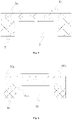
- Fig. 5 shows a schematic structural diagram of another embodiment of the micro-filter of the present disclosure.
- the metal film 6a is provided on the substrate 5 and is suspended above the hollow back cavity 7 of the substrate 5.
- the metal film 6a may be an amorphous metal film, for example, metallic glass.
- the substrate 5 may be made of polymer material, metal, silicon or SiO 2 .
- the outer surface of the metal film 6a is coated with a nonstick layer 6b.
- the adhesion between the nonstick layer 6b and the particles is lower than the adhesion between the metal film 6a and the particles; the metal film 6a and the nonstick layer 6b are arranged with through holes (not shown in the figures).
- the nonstick layer 6b is a silicone compound coating or a fluoropolymer coating.
- the nonstick layer 6b is a Teflon coating. Teflon has high temperature characteristic and a low coefficient of friction.
- the metal film 6a is configured to have compressive stress; the nonstick layer 6b is configured to have tensile stress; by compounding the metal film 6a and the nonstick layer 6b together, it is possible to reduce the stress of the entire film.
- the metal film 6a is configured to have tensile stress, and the nonstick layer 6b is configured to have compressive stress.
- the specific principle is the same as the embodiment shown in FIG. 2 and FIG. 4 , and will not be described in detail herein.
- the stress of the composite film layers is controlled between -300 MPa (compressive stress) and 300 MPa (tensile stress).
- the stress of the composite film layers is controlled between 0 and 300 MPa (tensile stress).
- Fig. 6 shows a schematic structural diagram of another embodiment of the micro-filter of the present disclosure.
- the film layer on the substrate 50 includes a three-layer diaphragm that is suspended above the hollow back cavity 70 of the substrate 50.
- the three-layer diaphragm includes one layer of the metal film 60a with compressive stress and two nonstick layers 60b with tensile stress.
- the metal film 60a is sandwiched between the two nonstick layers 60b, and the three layers are compounded together.
- the nonstick layers 60b with tensile stress located on both sides offset the compressive stress of the metal film located in the middle; conversely, the metal film 60a with compressive stress located in the middle also offsets compressive stress of the nonstick layers 60b on both sides, which will not be described in detail herein.
- nonstick layers 60b are provided on both sides of the metal film 60a, so that particle adsorption of the metal film 60a may be avoided or reduced, thereby ensuring the performance of the micro-filter.
Landscapes
- Engineering & Computer Science (AREA)
- Physics & Mathematics (AREA)
- Acoustics & Sound (AREA)
- Signal Processing (AREA)
- Multimedia (AREA)
- Chemical & Material Sciences (AREA)
- Chemical Kinetics & Catalysis (AREA)
- Micromachines (AREA)
- Laminated Bodies (AREA)
- Separation Using Semi-Permeable Membranes (AREA)
Applications Claiming Priority (2)
| Application Number | Priority Date | Filing Date | Title |
|---|---|---|---|
| CN201910579444.8A CN110267173B (zh) | 2019-06-28 | 2019-06-28 | 一种微型过滤器及声学设备 |
| PCT/CN2019/094776 WO2020258363A1 (fr) | 2019-06-28 | 2019-07-05 | Filtre miniature et dispositif acoustique |
Publications (4)
| Publication Number | Publication Date |
|---|---|
| EP3993441A1 true EP3993441A1 (fr) | 2022-05-04 |
| EP3993441A4 EP3993441A4 (fr) | 2023-08-02 |
| EP3993441B1 EP3993441B1 (fr) | 2025-12-10 |
| EP3993441C0 EP3993441C0 (fr) | 2025-12-10 |
Family
ID=67923217
Family Applications (1)
| Application Number | Title | Priority Date | Filing Date |
|---|---|---|---|
| EP19935734.4A Active EP3993441B1 (fr) | 2019-06-28 | 2019-07-05 | Filtre miniature et dispositif acoustique |
Country Status (4)
| Country | Link |
|---|---|
| US (1) | US11722808B2 (fr) |
| EP (1) | EP3993441B1 (fr) |
| CN (1) | CN110267173B (fr) |
| WO (1) | WO2020258363A1 (fr) |
Cited By (1)
| Publication number | Priority date | Publication date | Assignee | Title |
|---|---|---|---|---|
| JP2025069925A (ja) * | 2023-10-18 | 2025-05-01 | 玻音先創科技股▲ふん▼有限公司 | スピーカに適用される振動板 |
Families Citing this family (10)
| Publication number | Priority date | Publication date | Assignee | Title |
|---|---|---|---|---|
| CN110794499A (zh) * | 2019-10-31 | 2020-02-14 | 歌尔股份有限公司 | 滤光器 |
| CN110950299A (zh) * | 2019-10-31 | 2020-04-03 | 歌尔股份有限公司 | 微纳米结构组件制造方法、以及以该法制造的微纳米结构组件 |
| CN110775939A (zh) * | 2019-10-31 | 2020-02-11 | 歌尔股份有限公司 | 微纳米结构组件制造方法、以及以该法制造的微纳米结构组件 |
| CN110809207B (zh) * | 2019-10-31 | 2020-12-08 | 潍坊歌尔微电子有限公司 | 微型过滤器及mems传感器组件 |
| CN110775940B (zh) * | 2019-10-31 | 2023-08-15 | 潍坊歌尔微电子有限公司 | Mems传感器组件制造方法、以及以该法制造的mems传感器组件 |
| CN110933579B (zh) * | 2019-12-31 | 2025-03-18 | 潍坊歌尔微电子有限公司 | 防尘结构、麦克风封装结构以及电子设备 |
| CN111147993A (zh) * | 2019-12-31 | 2020-05-12 | 歌尔股份有限公司 | 防尘结构、麦克风封装结构以及电子设备 |
| CN110972046B (zh) * | 2019-12-31 | 2024-12-31 | 潍坊歌尔微电子有限公司 | 防尘结构、麦克风封装结构以及电子设备 |
| CN111787473A (zh) * | 2020-06-30 | 2020-10-16 | 歌尔微电子有限公司 | 微型麦克风颗粒阻拦器及mems麦克风 |
| CN112492476B (zh) * | 2020-12-02 | 2022-08-09 | 潍坊歌尔微电子有限公司 | 微型麦克风防尘装置及mems麦克风 |
Family Cites Families (10)
| Publication number | Priority date | Publication date | Assignee | Title |
|---|---|---|---|---|
| US6110544A (en) * | 1997-06-26 | 2000-08-29 | General Electric Company | Protective coating by high rate arc plasma deposition |
| CN1901758A (zh) * | 2005-07-19 | 2007-01-24 | 青岛歌尔电子有限公司 | 电容式硅传声器 |
| US9716050B2 (en) * | 2010-01-04 | 2017-07-25 | Crucible Intellectual Property, Llc | Amorphous alloy bonding |
| CN105120415A (zh) * | 2015-07-25 | 2015-12-02 | 刘南林 | 一种超级声波传感器震动膜制造技术 |
| CN206008239U (zh) * | 2016-07-29 | 2017-03-15 | 浙江华基环保科技有限公司 | 一种复合过滤布 |
| WO2018064803A1 (fr) * | 2016-10-08 | 2018-04-12 | Goertek. Inc | Dispositif de microphone mems et appareil électronique |
| TWI633194B (zh) * | 2017-05-24 | 2018-08-21 | Ming Chi University Of Technology | 聲學振膜及含此的揚聲裝置 |
| WO2018223389A1 (fr) * | 2017-06-09 | 2018-12-13 | Goertek. Inc | Microphone mems, son procédé de fabrication et appareil électronique |
| CN109379684B (zh) * | 2018-10-09 | 2020-05-29 | 歌尔股份有限公司 | 麦克风和电子设备 |
| CN109536748B (zh) * | 2019-01-04 | 2020-03-10 | 上海交通大学 | 金属玻璃微纳米带的制备方法及金属玻璃微纳米带 |
-
2019
- 2019-06-28 CN CN201910579444.8A patent/CN110267173B/zh active Active
- 2019-07-05 EP EP19935734.4A patent/EP3993441B1/fr active Active
- 2019-07-05 WO PCT/CN2019/094776 patent/WO2020258363A1/fr not_active Ceased
- 2019-07-05 US US17/623,304 patent/US11722808B2/en active Active
Cited By (1)
| Publication number | Priority date | Publication date | Assignee | Title |
|---|---|---|---|---|
| JP2025069925A (ja) * | 2023-10-18 | 2025-05-01 | 玻音先創科技股▲ふん▼有限公司 | スピーカに適用される振動板 |
Also Published As
| Publication number | Publication date |
|---|---|
| US11722808B2 (en) | 2023-08-08 |
| EP3993441A4 (fr) | 2023-08-02 |
| EP3993441B1 (fr) | 2025-12-10 |
| CN110267173B (zh) | 2021-01-22 |
| EP3993441C0 (fr) | 2025-12-10 |
| WO2020258363A1 (fr) | 2020-12-30 |
| CN110267173A (zh) | 2019-09-20 |
| US20220377442A1 (en) | 2022-11-24 |
Similar Documents
| Publication | Publication Date | Title |
|---|---|---|
| EP3993441B1 (fr) | Filtre miniature et dispositif acoustique | |
| WO2020258364A1 (fr) | Microfiltre et dispositif acoustique | |
| WO2020258362A1 (fr) | Microfiltre et dispositif acoustique | |
| CN101631739B (zh) | 用于制造mems麦克风的方法 | |
| WO2020258361A1 (fr) | Microfiltre et dispositif acoustique | |
| CN208063457U (zh) | 微机电系统(mems)换能器和微机电系统(mems)麦克风组件 | |
| WO2017206813A1 (fr) | Microphone mems et procédé de préparation associé | |
| US20180002161A1 (en) | Mems device and process | |
| GB2555510A (en) | MEMS device and process | |
| CN110958549A (zh) | 用于mems器件的防尘结构及mems麦克风封装结构 | |
| CN110809207B (zh) | 微型过滤器及mems传感器组件 | |
| US10343894B2 (en) | MEMS device and process | |
| US11212621B2 (en) | Composite diaphragms having balanced stress | |
| CN111816567A (zh) | 一种双面厚膜电镀铜散热结构制作方法 | |
| CN105989929A (zh) | 一种导电薄膜制作方法及导电薄膜 | |
| CN110775940B (zh) | Mems传感器组件制造方法、以及以该法制造的mems传感器组件 | |
| CN121521249A (zh) | 适用于深海高压环境的压电式水听器及其制备方法 | |
| Nayak et al. | PRODUCTIZATION CHALLENGES OF ACOUSTIC MEMS SENSORS AND ACTUATORS | |
| WO2021082054A1 (fr) | Procédé de fabrication d'ensemble micro/nano-structure et ensemble micro/nano-structure fabriqué par le procédé | |
| CN110759313A (zh) | Mems传感器组件制造方法以及以该法制造的传感器组件 | |
| CN110775939A (zh) | 微纳米结构组件制造方法、以及以该法制造的微纳米结构组件 | |
| TW202113948A (zh) | 薄型線路製作方法 | |
| JP2002043584A (ja) | ダイヤフラム構造体、微小トランスジューサ、およびこれらの製造方法 | |
| JPH01295169A (ja) | 複合振動板とその製造方法および複合振動板を用いた圧電型加速度センサ |
Legal Events
| Date | Code | Title | Description |
|---|---|---|---|
| STAA | Information on the status of an ep patent application or granted ep patent |
Free format text: STATUS: THE INTERNATIONAL PUBLICATION HAS BEEN MADE |
|
| PUAI | Public reference made under article 153(3) epc to a published international application that has entered the european phase |
Free format text: ORIGINAL CODE: 0009012 |
|
| STAA | Information on the status of an ep patent application or granted ep patent |
Free format text: STATUS: REQUEST FOR EXAMINATION WAS MADE |
|
| 17P | Request for examination filed |
Effective date: 20211223 |
|
| AK | Designated contracting states |
Kind code of ref document: A1 Designated state(s): AL AT BE BG CH CY CZ DE DK EE ES FI FR GB GR HR HU IE IS IT LI LT LU LV MC MK MT NL NO PL PT RO RS SE SI SK SM TR |
|
| DAV | Request for validation of the european patent (deleted) | ||
| DAX | Request for extension of the european patent (deleted) | ||
| REG | Reference to a national code |
Ref country code: DE Ref legal event code: R079 Free format text: PREVIOUS MAIN CLASS: H04R0009060000 Ipc: H04R0001080000 Ref document number: 602019079192 Country of ref document: DE |
|
| A4 | Supplementary search report drawn up and despatched |
Effective date: 20230704 |
|
| RIC1 | Information provided on ipc code assigned before grant |
Ipc: H04R 1/02 20060101ALI20230628BHEP Ipc: H04R 1/08 20060101AFI20230628BHEP |
|
| GRAP | Despatch of communication of intention to grant a patent |
Free format text: ORIGINAL CODE: EPIDOSNIGR1 |
|
| STAA | Information on the status of an ep patent application or granted ep patent |
Free format text: STATUS: GRANT OF PATENT IS INTENDED |
|
| INTG | Intention to grant announced |
Effective date: 20250716 |
|
| GRAS | Grant fee paid |
Free format text: ORIGINAL CODE: EPIDOSNIGR3 |
|
| GRAA | (expected) grant |
Free format text: ORIGINAL CODE: 0009210 |
|
| STAA | Information on the status of an ep patent application or granted ep patent |
Free format text: STATUS: THE PATENT HAS BEEN GRANTED |
|
| AK | Designated contracting states |
Kind code of ref document: B1 Designated state(s): AL AT BE BG CH CY CZ DE DK EE ES FI FR GB GR HR HU IE IS IT LI LT LU LV MC MK MT NL NO PL PT RO RS SE SI SK SM TR |
|
| REG | Reference to a national code |
Ref country code: CH Ref legal event code: F10 Free format text: ST27 STATUS EVENT CODE: U-0-0-F10-F00 (AS PROVIDED BY THE NATIONAL OFFICE) Effective date: 20251210 Ref country code: GB Ref legal event code: FG4D |
|
| REG | Reference to a national code |
Ref country code: DE Ref legal event code: R096 Ref document number: 602019079192 Country of ref document: DE |
|
| REG | Reference to a national code |
Ref country code: IE Ref legal event code: FG4D |
|
| U01 | Request for unitary effect filed |
Effective date: 20260105 |
|
| U07 | Unitary effect registered |
Designated state(s): AT BE BG DE DK EE FI FR IT LT LU LV MT NL PT RO SE SI Effective date: 20260113 |
|
| PG25 | Lapsed in a contracting state [announced via postgrant information from national office to epo] |
Ref country code: ES Free format text: LAPSE BECAUSE OF FAILURE TO SUBMIT A TRANSLATION OF THE DESCRIPTION OR TO PAY THE FEE WITHIN THE PRESCRIBED TIME-LIMIT Effective date: 20251210 |
|
| PG25 | Lapsed in a contracting state [announced via postgrant information from national office to epo] |
Ref country code: NO Free format text: LAPSE BECAUSE OF FAILURE TO SUBMIT A TRANSLATION OF THE DESCRIPTION OR TO PAY THE FEE WITHIN THE PRESCRIBED TIME-LIMIT Effective date: 20260310 |
|
| PG25 | Lapsed in a contracting state [announced via postgrant information from national office to epo] |
Ref country code: HR Free format text: LAPSE BECAUSE OF FAILURE TO SUBMIT A TRANSLATION OF THE DESCRIPTION OR TO PAY THE FEE WITHIN THE PRESCRIBED TIME-LIMIT Effective date: 20251210 |
|
| PG25 | Lapsed in a contracting state [announced via postgrant information from national office to epo] |
Ref country code: RS Free format text: LAPSE BECAUSE OF FAILURE TO SUBMIT A TRANSLATION OF THE DESCRIPTION OR TO PAY THE FEE WITHIN THE PRESCRIBED TIME-LIMIT Effective date: 20260310 |