EP3994710B1 - Ntc-dünnschichtthermistor und verfahren zur herstellung eines ntc-dünnschichtthermistors - Google Patents
Ntc-dünnschichtthermistor und verfahren zur herstellung eines ntc-dünnschichtthermistors Download PDFInfo
- Publication number
- EP3994710B1 EP3994710B1 EP20739589.8A EP20739589A EP3994710B1 EP 3994710 B1 EP3994710 B1 EP 3994710B1 EP 20739589 A EP20739589 A EP 20739589A EP 3994710 B1 EP3994710 B1 EP 3994710B1
- Authority
- EP
- European Patent Office
- Prior art keywords
- thin film
- ntc
- thermistor
- electrodes
- thin
- Prior art date
- Legal status (The legal status is an assumption and is not a legal conclusion. Google has not performed a legal analysis and makes no representation as to the accuracy of the status listed.)
- Active
Links
Images


Classifications
-
- H—ELECTRICITY
- H01—ELECTRIC ELEMENTS
- H01C—RESISTORS
- H01C7/00—Non-adjustable resistors formed as one or more layers or coatings; Non-adjustable resistors made from powdered conducting material or powdered semi-conducting material with or without insulating material
- H01C7/04—Non-adjustable resistors formed as one or more layers or coatings; Non-adjustable resistors made from powdered conducting material or powdered semi-conducting material with or without insulating material having negative temperature coefficient
- H01C7/042—Non-adjustable resistors formed as one or more layers or coatings; Non-adjustable resistors made from powdered conducting material or powdered semi-conducting material with or without insulating material having negative temperature coefficient mainly consisting of inorganic non-metallic substances
-
- H—ELECTRICITY
- H01—ELECTRIC ELEMENTS
- H01C—RESISTORS
- H01C7/00—Non-adjustable resistors formed as one or more layers or coatings; Non-adjustable resistors made from powdered conducting material or powdered semi-conducting material with or without insulating material
- H01C7/04—Non-adjustable resistors formed as one or more layers or coatings; Non-adjustable resistors made from powdered conducting material or powdered semi-conducting material with or without insulating material having negative temperature coefficient
- H01C7/041—Non-adjustable resistors formed as one or more layers or coatings; Non-adjustable resistors made from powdered conducting material or powdered semi-conducting material with or without insulating material having negative temperature coefficient formed with two or more layers
-
- H—ELECTRICITY
- H01—ELECTRIC ELEMENTS
- H01C—RESISTORS
- H01C1/00—Details
- H01C1/14—Terminals or tapping points specially adapted for resistors; Arrangements of terminals or tapping points on resistors
-
- H—ELECTRICITY
- H01—ELECTRIC ELEMENTS
- H01C—RESISTORS
- H01C1/00—Details
- H01C1/14—Terminals or tapping points specially adapted for resistors; Arrangements of terminals or tapping points on resistors
- H01C1/142—Terminals or tapping points specially adapted for resistors; Arrangements of terminals or tapping points on resistors the terminals or tapping points being coated on the resistive element
-
- H—ELECTRICITY
- H01—ELECTRIC ELEMENTS
- H01C—RESISTORS
- H01C17/00—Apparatus or processes specially adapted for manufacturing resistors
- H01C17/06—Apparatus or processes specially adapted for manufacturing resistors adapted for coating resistive material on a base
-
- H—ELECTRICITY
- H01—ELECTRIC ELEMENTS
- H01C—RESISTORS
- H01C17/00—Apparatus or processes specially adapted for manufacturing resistors
- H01C17/06—Apparatus or processes specially adapted for manufacturing resistors adapted for coating resistive material on a base
- H01C17/075—Apparatus or processes specially adapted for manufacturing resistors adapted for coating resistive material on a base by thin-film techniques
-
- H—ELECTRICITY
- H01—ELECTRIC ELEMENTS
- H01C—RESISTORS
- H01C17/00—Apparatus or processes specially adapted for manufacturing resistors
- H01C17/28—Apparatus or processes specially adapted for manufacturing resistors adapted for applying terminals
- H01C17/288—Apparatus or processes specially adapted for manufacturing resistors adapted for applying terminals by thin film techniques
-
- H—ELECTRICITY
- H01—ELECTRIC ELEMENTS
- H01C—RESISTORS
- H01C17/00—Apparatus or processes specially adapted for manufacturing resistors
- H01C17/30—Apparatus or processes specially adapted for manufacturing resistors adapted for baking
-
- H—ELECTRICITY
- H01—ELECTRIC ELEMENTS
- H01C—RESISTORS
- H01C7/00—Non-adjustable resistors formed as one or more layers or coatings; Non-adjustable resistors made from powdered conducting material or powdered semi-conducting material with or without insulating material
- H01C7/006—Thin film resistors
-
- H—ELECTRICITY
- H01—ELECTRIC ELEMENTS
- H01C—RESISTORS
- H01C7/00—Non-adjustable resistors formed as one or more layers or coatings; Non-adjustable resistors made from powdered conducting material or powdered semi-conducting material with or without insulating material
- H01C7/18—Non-adjustable resistors formed as one or more layers or coatings; Non-adjustable resistors made from powdered conducting material or powdered semi-conducting material with or without insulating material comprising a plurality of layers stacked between terminals
-
- H—ELECTRICITY
- H05—ELECTRIC TECHNIQUES NOT OTHERWISE PROVIDED FOR
- H05K—PRINTED CIRCUITS; CASINGS OR CONSTRUCTIONAL DETAILS OF ELECTRIC APPARATUS; MANUFACTURE OF ASSEMBLAGES OF ELECTRICAL COMPONENTS
- H05K1/00—Printed circuits
- H05K1/18—Printed circuits structurally associated with non-printed electric components
- H05K1/182—Printed circuits structurally associated with non-printed electric components associated with components mounted in printed circuit boards [PCB], e.g. insert-mounted components [IMC]
-
- H—ELECTRICITY
- H05—ELECTRIC TECHNIQUES NOT OTHERWISE PROVIDED FOR
- H05K—PRINTED CIRCUITS; CASINGS OR CONSTRUCTIONAL DETAILS OF ELECTRIC APPARATUS; MANUFACTURE OF ASSEMBLAGES OF ELECTRICAL COMPONENTS
- H05K1/00—Printed circuits
- H05K1/02—Details
- H05K1/03—Use of materials for the substrate
- H05K1/0306—Inorganic insulating substrates, e.g. ceramic, glass
-
- H—ELECTRICITY
- H05—ELECTRIC TECHNIQUES NOT OTHERWISE PROVIDED FOR
- H05K—PRINTED CIRCUITS; CASINGS OR CONSTRUCTIONAL DETAILS OF ELECTRIC APPARATUS; MANUFACTURE OF ASSEMBLAGES OF ELECTRICAL COMPONENTS
- H05K2201/00—Indexing scheme relating to printed circuits covered by H05K1/00
- H05K2201/06—Thermal details
- H05K2201/068—Thermal details wherein the coefficient of thermal expansion is important
-
- H—ELECTRICITY
- H05—ELECTRIC TECHNIQUES NOT OTHERWISE PROVIDED FOR
- H05K—PRINTED CIRCUITS; CASINGS OR CONSTRUCTIONAL DETAILS OF ELECTRIC APPARATUS; MANUFACTURE OF ASSEMBLAGES OF ELECTRICAL COMPONENTS
- H05K2201/00—Indexing scheme relating to printed circuits covered by H05K1/00
- H05K2201/10—Details of components or other objects attached to or integrated in a printed circuit board
- H05K2201/10007—Types of components
- H05K2201/10151—Sensor
-
- H—ELECTRICITY
- H05—ELECTRIC TECHNIQUES NOT OTHERWISE PROVIDED FOR
- H05K—PRINTED CIRCUITS; CASINGS OR CONSTRUCTIONAL DETAILS OF ELECTRIC APPARATUS; MANUFACTURE OF ASSEMBLAGES OF ELECTRICAL COMPONENTS
- H05K2201/00—Indexing scheme relating to printed circuits covered by H05K1/00
- H05K2201/10—Details of components or other objects attached to or integrated in a printed circuit board
- H05K2201/10007—Types of components
- H05K2201/10196—Variable component, e.g. variable resistor
Definitions
- the invention relates to an NTC thin-film thermistor and a method for producing an NTC thin-film thermistor.
- NTC thermistors are resistors with negative temperature coefficients that are often used as sensors for measuring temperature in electronic devices.
- Advantageous ceramics for an NTC thermistor are presented.
- the examples show typical NTC thermistors in a multi-layer construction, in which the ceramics are processed into films that have a thickness of 20 to 50 ⁇ m, and the finished multi-layer NTC thermistors have an extension of a few millimeters in all three spatial directions.
- Such a size is not suitable for many applications. By significantly reducing their dimensions, not only can space be created for other components in the applications, but also completely new application possibilities and fields can be opened up.
- a thermistor that has an aluminum substrate and a thermistor thin film arranged on top of it.
- the thermistor thin film comprises a rare earth metal and a transition metal and has a perovskite crystal structure.
- Comb-shaped interlocking electrodes made of platinum are arranged on top of the thin film.
- the patent specification US 2013/328154 A1 shows a thermistor that has a metal substrate, a ceramic layer arranged thereon and two electrodes.
- the ceramic layer comprises an NTC ceramic material comprising a combination of the transition metals Mn, Ni, Fe, Ti, Co, Al and/or Zn.
- the electrodes have a thickness between 0.1 ⁇ m and 10 ⁇ m.
- the patent specification US 2004/216305 A1 shows a ceramic multilayer component, which can be an NTC thermistor.
- the multilayer component has internal electrodes and ceramic layers that can have a thickness of about 3 ⁇ m.
- NTC thermistors By making NTC thermistors extremely thin, they can be flexible and thus bent without causing mechanical damage. If an NTC thermistor with a small expansion is also made, This may increase its thermal mass and thus improve the response time and sensitivity of the NTC thermistor.
- NTC thermistor with a small dimension in all spatial directions as well as a particularly flat NTC thermistor.
- the object of the present invention is to provide an advantageous NTC thin-film thermistor and a method for producing an NTC thin-film thermistor.
- the present object is achieved by the NTC thin-film thermistor according to claim 1 and by a method for producing an NTC thin-film thermistor according to the further independent claim 19. Further advantageous embodiments, potential arrangements and possible method steps can be found in the further claims.
- An NTC thin-film thermistor which consists of at least one first thin-film electrode, at least one NTC thin film and at least one second thin-film electrode.
- the formation of the electrodes and the functional NTC layer as a thin film makes it possible to produce an NTC thermistor with an extremely small Expansion, especially with regard to thickness.
- a thin film can be understood to mean, in particular, layers that consist of solid materials in the micrometer range. Alternatively or additionally, a thin film can be understood to mean a layer with a thickness of less than 10 ⁇ m.
- An NTC thin film thermistor according to the present invention can preferably have exclusively thin film electrodes and thin films and no other types of layers.
- NTC thermistor By significantly reducing the dimensions of an NTC thermistor, not only can space be created for other components in the application, but completely new applications and fields can also be opened up. For example, by making NTC thermistors extremely thin, they can be flexible and thus bent without causing mechanical damage. In addition, if an NTC thermistor is made with a small expansion, this reduces its thermal mass and can therefore improve the response time and sensitivity of a sensor that has the NTC thermistor.
- the NTC thin film comprises a monocrystalline or polycrystalline functional ceramic that has a spinel structure or a perovskite structure.
- Such materials have a characteristic nonlinear temperature coefficient that enables accurate temperature measurement.
- functional ceramics with a perovskite structure are particularly suitable for use at high temperatures, as the electrical properties of perovskite structures are less affected at high temperatures than spinel structures.
- the thin-film electrodes can be made of a conductive ceramic.
- a conductive ceramic adheres more strongly to a functional ceramic than alternative materials such as a metal.
- a thin-film electrode made of a conductive ceramic has a similar thermal expansion coefficient to a functional ceramic, which can prevent mechanical stress in the NTC thin-film thermistor when the temperature changes.
- the thin-film electrodes can consist of one or more layers of metals such as Cu, Pt, Cr, Ni, Ag, Pd, Au, Ti or a mixture, an intermetallic compound or an alloy of these elements.
- Thin-film electrodes made of metal have a high electrical conductivity, which means that the NTC thin-film thermistor can have a lower electrical connection resistance.
- the first and second thin-film electrodes can be arranged on a surface of the NTC thin film.
- the NTC thin film thermistor can be made thinner than in an embodiment in which the NTC thin film is arranged between the first and second electrodes.
- a measuring current runs along the NTC thin film and not perpendicular to the layer. Since the dimensions of the surface of the functional NTC thin film can be a multiple of the thickness of the NTC thin film, an NTC thin film thermistor designed in this way can demonstrate more precise measuring accuracy.
- the first and second thin-film electrodes can be arranged in an interdigital comb structure on a surface. Since the electrodes in a conventional comb structure are equidistant from one another, the same electric field acts between the electrodes for a given measuring voltage. Therefore, the measuring current of an NTC thin-film thermistor provided with electrodes having an interdigital comb structure has an advantageous linearity with respect to an applied measuring voltage.
- the NTC thin-film thermistor has a plurality of first and second thin-film electrodes, wherein an NTC thin film is arranged between the first thin-film electrodes and the second thin-film electrodes.
- the measuring current runs perpendicular to the surface of the NTC thin films. Therefore, the lateral Expansion of the entire NTC thin-film thermistor in contrast to an NTC thin-film thermistor, the first and second electrode on a surface of the NTC thin film, can be much lower. By stacking several NTC thin films on top of each other, the measurement accuracy of the NTC thin film thermistor can be increased.
- first and second thin-film electrodes can rest on a respective underlying first or second thin-film electrode, which also overhangs the NTC thin film, in an area in which they overhang the NTC thin film.
- the thin-film electrode resting on top can be shaped to match the thin-film electrode underneath. Due to thin-film electrodes that have already been applied, the surface texture or topography in the areas that overhang the NTC thin-film electrode can have unevenness or inclinations. By resting the thin-film electrodes on the thin-film electrodes underneath in a shape-matched manner, these unevenness or inclinations are reproduced and the electrical contact area and the adhesion between adjacent thin-film electrodes are increased. This ensures that each of the thin-film electrodes is electrically contacted.
- first and second thin-film electrodes can be shorter in an area in which they overhang the NTC thin film than the underlying first or second thin-film electrodes that overhang the NTC thin film.
- a staircase shape is formed by the thin-film electrodes, which tapers the component in the thickness direction.
- Each thin-film electrode forms a step. Since each thin-film electrode forms a contact surface, analogous to the step, each individual thin-film electrode can be directly electrically contacted. This reduces the risk that an internal electrode arranged inside the NTC sensor remains electrically isolated and is not functional.
- the contact surface of the individual thin-film electrodes and also of the entire NTC sensor can be increased by shortening the thin-film electrodes even further compared to an underlying thin-film electrode. This leaves a larger surface of the underlying thin-film electrode, which can be used as a contact surface for electrical contact.
- the contact resistance of the component is reduced. Due to the characteristic of an NTC resistor, according to which the resistance decreases with increasing temperature, a low Contact resistance is particularly advantageous for accurate measurements in high temperature ranges.
- the first thin-film electrodes on a first side of the NTC thin-film thermistor overhang the NTC thin film
- the second NTC thin-film electrodes on the first side being shortened compared to the NTC thin film
- the second thin-film electrodes overhang the NTC thin film on a second side of the NTC thin-film thermistor, which is opposite the first side, and the first thin-film electrodes are shortened compared to the NTC thin film on the second side.
- a step shape is formed on a first and second side of the NTC thin-film thermistor, which tapers the component in the direction of thickness.
- the individual thin-film electrodes overlap on this side and can thus be contacted together. Since the other electrode on this side is shortened compared to the NTC thin film, there is always an NTC thin film between the electrodes, thus preventing a short circuit between the first and second electrodes.
- the protruding portions of the first and second thin-film electrodes on the first and second sides can be reinforced with a metallized paste or another conductive medium.
- the electrodes in these portions are nevertheless extremely thin and fragile.
- a metallized paste can be applied to the overlapping portion. to reinforce the electrodes and facilitate contact between the electrodes.
- the NTC thin films can overhang the thin film electrodes on a third and fourth side, which are perpendicular to the first and second sides and face each other.
- An overhang of the non-conductive NTC thin film ensures that the first and second thin film electrodes are also encapsulated from each other in the edge areas. In this way, it can be ensured that the first and second electrodes do not short-circuit despite the small distance between them.
- the NTC thin films can be shorter than the underlying NTC thin film in an area where they overhang the thin film electrodes. This creates a diagonal edge of the NTC thin film thermistor on the sides where the NTC thin film overhangs.
- a truncated pyramid design of the NTC thin film thermistor offers a low center of gravity, which makes the component more stable.
- the NTC thin-film thermistor can also be arranged on a carrier material.
- the carrier material can increase the mechanical stability of the NTC thin-film thermistor. High mechanical stability is particularly important for transporting and installing the component in order to avoid damage.
- the component can therefore be arranged on a carrier material.
- the carrier material can already be designed as a first electrode.
- a thicker conductive ceramic layer or a stable metal layer can be used as carrier material. This avoids the need for additional carrier material.
- a circuit or a microelectronic mechanical system can be integrated into the carrier material, or the carrier material can be a component of an electronic component.
- the NTC thin-film thermistor can be integrated and contacted with an electrical component.
- electrical components made of semiconductors such as silicon electrical components made of ceramics are extremely suitable for the integration of an NTC thin-film thermistor, as they have a similar thermal expansion coefficient to the NTC thin-film thermistor.
- a protective layer can be applied to the NTC thin-film thermistor or the entire component can be embedded in a protective layer to protect the component from mechanical, chemical and other environmental influences.
- Glass, silicone or other polymers can be suitable materials for the protective layer.
- the NTC thin film can be thinner than 3 ⁇ m. This makes it possible to have a thin design of the NTC thin film thermistor, even with several NTC thin films. It should also be noted that the NTC thin film must be thick enough to avoid a short circuit between electrodes. A thickness of over 0.01 ⁇ m is therefore advisable for typical voltage ranges and materials.
- the thin-film electrodes can be thinner than 10 ⁇ m. If the thin-film electrodes were made much thicker, a thin design of the NTC thin-film thermistor could be prevented.
- the entire NTC thin-film thermistor can be thinner than 100 ⁇ m. This ensures that the advantage of the individual very thin thin films is transferred to the entire component and the entire NTC thin-film thermistor remains very thin.
- the NTC thin-film thermistor may be suitable for integration into a substrate or a circuit board.
- Substrates and also circuit boards can often only have a thickness of a few 100 ⁇ m. Since an NTC thin-film thermistor according to the present invention can be thinner, it can not only be mounted as an SMD component on a substrate or a circuit board, but can also be integrated into it.
- An advantageous arrangement can comprise a circuit board and an NTC thin-film thermistor, wherein the NTC thin-film thermistor is integrated into the circuit board. Consequently, not only can space on the circuit board be saved, which can be used for other components, but the integration of the NTC thin-film thermistor into the circuit board simultaneously expands its functionality.
- NTC thin-film thermistors can be arranged in a matrix. Due to the small size of the NTC thin-film thermistors, especially with regard to their required surface area, NTC thin-film thermistors are ideal for sensor applications where a spatially resolved temperature measurement is to be carried out. For this purpose, several NTC thin-film thermistors are arranged next to each other on a matrix.
- a further aspect of the present application relates to a method, as specified in claim 19, for producing an NTC thin-film thermistor.
- the NTC thin-film thermistor can in particular be the NTC thin-film thermistor described above.
- a non-conductive substrate may be required as a flat base on which to form the further layers. Only after at least one NTC thin film and at least one first and second thin film electrode have been completed is the NTC thin film thermistor functional.
- a circuit or a microelectronic mechanical system can be integrated into the carrier material, or the carrier material can be a component of an electronic component.
- an electrical component can be upgraded with an NTC thin-film thermistor. Thanks to the integrated design, the electrical component can be connected directly to the NTC thin-film thermistor and electrically contacted.
- Electrical components made of ceramics are particularly suitable as a carrier material because they have a similar thermal expansion coefficient to the NTC thin-film thermistor and the NTC thin-film thermistor adheres well to them. Electrical components, circuits and microelectronic mechanical systems made of semiconductors such as silicon can also be used as a carrier material.
- the first and second thin-film electrodes can be arranged on a surface of the NTC thin film.
- An NTC thin-film thermistor according to such a method can be made thinner than in a design in which the NTC thin film is arranged between the first and second electrodes.
- the measuring current runs along the NTC thin film and not perpendicularly through the layer. Due to the lateral dimensions of the NTC thin-film thermistor, which can be a multiple of the thickness of the NTC thin film, such an NTC thin-film thermistor can demonstrate more precise measurement accuracy.
- an NTC thin film is arranged between the first thin film electrodes and the second thin film electrodes.
- the measuring current runs perpendicular to the surface through the NTC thin films.
- the lateral extension of such an NTC thin film thermistor influences the Measurement accuracy is not very high. Therefore, an NTC thin film thermistor can have a much smaller expansion using these methods.
- the NTC thin films can be stacked on top of each other to improve the measurement accuracy of the NTC thin film thermistor.
- the method can also be carried out in such a way that in step b) the first thin-film electrodes are also applied in a first region in which there is no NTC thin film underneath, and that in step d) the second thin-film electrodes are also applied in a second region in which there is no NTC thin film underneath, wherein the first and second regions do not overlap with one another and the method contains a sequence of steps in which first a first thin-film electrode layer is applied, then an NTC thin film is applied, then a second thin-film electrode is applied, whereupon another NTC thin film is applied, and then another first thin-film electrode is applied.
- NTC thin-film thermistor manufactured using this method has the advantage that the thin-film electrodes arranged inside the NTC thin-film thermistor are electrically contacted more reliably, making the entire component more robust.
- the thin film electrodes in the two areas can also shorter than the first or second thin-film electrodes underneath. In this way, a staircase shape is formed in the first and second areas, with the individual steps being formed from the thin-film electrodes.
- the contact area of the thin-film electrodes can be increased and thus the contact resistance reduced.
- Such an NTC thin-film thermistor is particularly suitable for precise temperature measurements at high temperatures, since an NTC resistance decreases with increasing temperature.
- the NTC thin films can be applied in any of the processes listed using a CSD (chemical solution deposition) process.
- CSD chemical solution deposition
- spin coating, dip coating or ink jet printing each of which is a CSD process, can be used.
- Ink jet printing has the advantage that the NTC thin films can be adapted modularly and the process is more variable.
- both the first and second thin-film electrodes and the NTC thin films can be applied in the above-mentioned processes using a PVD or CVD process. This ensures that all layers can be formed as thin films.
- the NTC thin-film thermistor can be subjected to a sintering process in a further process step.
- the sintering process makes the NTC thin film, which is usually available as functional ceramic, more mechanically resilient and resistant to deformation.
- a perovskite or spinel structure can often only be formed during a cooling process.
- the NTC thin-film thermistor can be detached from the carrier material, or the carrier material can be thinned out or completely removed using a grinding or etching process. Consequently, for each NTC thin-film thermistor, it can be decided whether a small thickness or a certain mechanical stability of the NTC thin-film thermistor is more important. Depending on preference, the thickness of the carrier material can be reduced to a desired level, or the NTC thin-film thermistor can be detached directly from the carrier material.
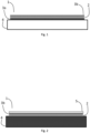
- FIG. 1 a cross-sectional view of an NTC thin-film thermistor 1 is shown.
- a first thin-film electrode 3a, above this an NTC thin film 2 and above this a second thin-film electrode 3b are arranged on a carrier material 4.
- the carrier material 4 is electrically insulating and flat.
- a certain thermal stability of the carrier material 4 is required for possible thermal process steps for producing the thin films, in which temperatures of over 500 °C can be reached.
- Suitable insulating and thermally stable materials for the carrier material 4 are polycrystalline or monocrystalline ceramics, passivated semiconductors, polymers or glass.
- the polycrystalline or monocrystalline ceramics can be, for example, YSZ, AlN, ZnO, aluminum oxide or sapphire
- the passivated semiconductors can be, for example, monocrystalline silicon with SiOx passivation
- the polymers can be, for example, a polyimide.
- the carrier material 4 is preferably very thin, with a thickness of no more than 100 ⁇ m and no less than 1 ⁇ m, but it can also be significantly thicker.
- the term thickness is used here and below to refer to the extent in the stacking direction, i.e. perpendicular to the surface of the layers.
- the first thin-film electrode 3a, the NTC thin-film 2 and the second thin-film electrode 3b are arranged one above the other in the stacking direction.
- the NTC thin-film thermistor 1 can be detached from the carrier material 4 after production or the carrier material 4 can be thinned out. Known etching or grinding processes can be used for this purpose.
- the carrier material 4 can also have functional properties and comprise, for example, an integrated circuit (IC) or a micro-electrical mechanical system (MEMS).
- IC integrated circuit
- MEMS micro-electrical mechanical system
- the NTC thin-film thermistor 1 can be connected to at least one other electrical component, for example a pressure sensor or a piezoelectric sensor, and thus different functions can be combined in one electrical component.
- the first and second thin-film electrodes 3a, 3b are made of Figure 1 above and below the active NTC thin film 2.
- the thin film electrodes 3a, 3b are preferably very thin, with a thickness of less than 10 ⁇ m. Chemical and physical deposition processes for thin films, such as PVD, CVD, CSD or galvanic processes, are suitable for forming the thin film electrodes 3a, 3b, depending on the material used.
- the electrodes can consist of one or more layers and of the same or different materials. Different electrodes and electrode layers can, but do not have to, be made of the same material. Suitable conductive materials for the electrodes are metals, alloys, intermetallic compounds or conductive ceramics.
- the metals can be, for example, Cu, Ni, Ag, Au, Pt, Mo or Wo.
- the alloys can be, for example, Cr/Ni/Ag or Cr/Au.
- the intermetallic compounds can be titanium, nickel or molybdenum silicides.
- the conductive ceramics can be, for example, LNO or ITO.
- the NTC thin film 2 is thinner than 3 ⁇ m, preferably even thinner than 1 ⁇ m, and is applied using one or more coating and thermal process steps.
- a suitable coating process for NTC thin films 2 is a CSD process in which the layer is applied, for example, using spin coating, dip coating, spray coating or ink jet printing. Deposition of the NTC thin film 2 using a PVD process is also possible.
- the NTC thin film 2 consists of a single- or multi-phase functional ceramic that has a spinel or perovskite structure. Suitable elements for an NTC thin film 2 with a spinel structure are Ni, Mn, Co, Fe, Cu and Zr.
- Figure 2 shows a second embodiment of the invention, which corresponds to the example of Figure 1
- three layers are also applied to a carrier material 4 applied one above the other.
- the carrier material 4 here is also simultaneously a first electrode or bottom electrode.
- An NTC thin film 2, a second thin film electrode 3b and a protective layer 5 are applied one above the other on the carrier material 4, which also functions as the first electrode.
- the carrier material 4 is sufficiently conductive to serve as a bottom electrode. Suitable materials are metals, alloys or highly doped semiconductors. Insulators coated with conductive material can also be used. In particular, the carrier material 4 can also be present as a conductive ceramic. This makes it particularly easy to connect the NTC thin-film thermistor 1 to another electrical component which itself has a conductive ceramic. In this way, two or more functions of different components can be combined and integrated into one component.
- the protective layer 5 is an electrically passive layer that protects the NTC thin-film thermistor 1 from mechanical, chemical and other environmental influences.
- a thin-film process can be used as with the other thin films, especially a PVD process.
- the NTC thin-film sensor 2 can also be glued or welded into a film.
- Suitable materials for the protective layer 5 can be glass, silicone or other polymers.
- the protective layer 5 does not necessarily have to be Figure 2 shown, be applied to one side of the NTC thin-film thermistor 1, but can enclose the NTC thin-film thermistor 1. Particularly It is advantageous to completely enclose the NTC thin-film thermistor 1 in a protective layer 5 if it is detached from the carrier material 4 or is designed to be particularly thin.
- Figure 3 shows another example, which is similar to the example from Figure 2 Three layers are stacked on a carrier material 4.
- the carrier material 4 is not conductive and therefore does not act as an electrode.
- An NTC thin film 2 was applied to the carrier material 4.
- Both the first and second thin film electrodes 3a, 3b were applied directly to the NTC thin film 2, whereby in Figure 3 only one thin-film electrode 3a, 3b is visible.
- the thin-film electrodes 3a, 3b and the NTC thin film 2 were also protected against environmental influences by a protective layer 5.
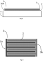
- FIG 4 a plan view of an NTC thin-film thermistor 1 is shown, in which, as in the embodiment of Figure 3 both electrodes are arranged on the NTC thin film 2.
- the first and second thin film electrodes 3a, 3b are arranged in an interdigital comb structure. Since the thin film electrodes 3a, 3b are equidistant from each other, the same electric field acts between the thin film electrodes 3a, 3b when a measuring voltage is applied. Therefore, the measuring current of an NTC thin film thermistor 1, which is provided with thin film electrodes 3a, 3b, which have an interdigital comb structure, has an advantageous linearity with respect to an applied measuring voltage.
- the electrode structure can either be formed directly when depositing the Thin film electrodes 3a, 3b can be applied to the NTC thin film 2 by means of a shadow mask or via a lithographic process afterwards. Depending on the desired resistance and the design of the NTC thin film thermistor 1, a different arrangement of the thin film electrodes 3a, 3b may be more appealing.
- the NTC thin film thermistor 1 can be made particularly thin with a thickness of less than 50 ⁇ m.
- the requirement for the quality of the NTC thin film 2 can be lower because the measuring current flows relatively far along the surface and vertical defects in the NTC thin film 2 have little influence on it.
- FIG. 5 a cross-sectional view of an embodiment according to the present invention is shown.
- the NTC thin-film thermistor 1 is a multi-layer component.
- the first and second thin-film electrodes 3a, 3b have been applied alternately to the non-conductive carrier material 4, with an NTC thin film 2 always lying between them.
- one type of thin-film electrode 3a, 3b overhangs the NTC thin film 2, whereas the other type is shortened compared to the NTC thin film 2.
- the thin-film electrodes 3a, 3b of one type can be easily connected to one another and at the same time a short circuit with the counter thin-film electrode can be prevented.
- the electrical contact is made via the increased contact surface between the adjacent thin-film electrodes. improved and the risk that one of the thin-film electrodes is not electrically contacted is reduced.
- the internal electrodes of the multilayer NTC thin-film thermistor 1 may be advantageous to form from a conductive ceramic, since this adheres well to the functional ceramic NTC thin films 2 and the entire active element of the NTC thin-film thermistor 1 is made entirely of ceramic. In this case, it may still be advantageous to form a bottom and a top electrode of the multilayer structure from a metal or another conductive material.
- a step shape is formed on a first and second side of the NTC thin-film thermistor 1, which tapers the component in the direction of thickness.
- the thin-film electrodes 3a, 3b in the area in which they overhang the NTC thin film 2, can be shortened compared to the underlying thin-film electrode 3a, 3b.
- the contact surface of the thin-film electrodes 3a, 3b can thus be increased and the contact resistance of the NTC thin-film thermistor 1 can be reduced.
- An NTC thin-film thermistor 1 with low contact resistance is particularly suitable for precise measurements in high temperature ranges, since an NTC resistance decreases with increasing temperature.
- the area in the middle, where all three types of layers overlap, is the active measuring area of the NTC thin-film thermistor 1.
- the areas in which only one type of thin-film electrode alternates with the NTC thin-film 2 are irrelevant from a measurement point of view and should be kept as small as possible.
- the electrodes can be contacted at the edges where the thin-film electrodes 3a, 3b are brought together.
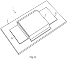
- Figure 6 shows a spatial representation of an NTC thin-film thermistor 1, which also has a multilayer structure like the NTC thin-film thermistor 1 from Figure 5 and is arranged on a carrier material 4.
- the NTC thin films 2 overhang on a third and fourth side, which are perpendicular to the first and second side, opposite the thin film electrodes 3a, 3b.
- the overhanging NTC material forms sloping slopes on the third and fourth side in Figure 6
- the overhang of the NTC thin films 2 ensures that the first and second thin film electrodes 3a, 3b are also encapsulated from one another in the edge areas.
- the first and second thin film electrodes 3a, 3b do not short-circuit with one another. Since the thin film electrodes 3a, 3b are still very thin at the edges, even though several layers are superimposed, it is advisable to reinforce the electrodes with a metallic paste, contact pads, a screen printing process, a thin film process or a galvanic process.
- the NTC thin-film thermistor 1 is made of Figure 6 with additional contact pads.
- the described layer structure means that the measuring current in these embodiments flows vertically through the NTC layer, in contrast to the embodiment in which the thin-film electrodes 3a, 3b are arranged on a surface of the NTC thin film 2.
- this increases the demand on the quality of the NTC thin film 2 increased because defects have a greater effect on the measuring current, on the other hand, the measuring accuracy is not dependent on the size of the surface of the NTC thin film 2. Therefore, with the layer structure, NTC thin film thermistors 1 can be realized which, with a base area whose side length is between 80 and 120 ⁇ m and a thickness of less than 100 ⁇ m, are not only extremely thin, but also have a small surface.
- NTC thin-film thermistors 1 can be used, for example, in spatially resolved measurements. If several NTC thin-film thermistors 1 according to one of the embodiments are arranged in a matrix, a spatially resolved temperature measurement can be carried out with this arrangement. In addition, electrical components with such a small size are predestined to be connected to or integrated into other electrical components. In particular, the NTC thin-film thermistors 1 according to the present invention can also be integrated into circuit boards, which often only have a thickness of a few 100 ⁇ m, and do not have to be mounted on them.
Landscapes
- Engineering & Computer Science (AREA)
- Microelectronics & Electronic Packaging (AREA)
- Physics & Mathematics (AREA)
- Electromagnetism (AREA)
- Manufacturing & Machinery (AREA)
- Thermistors And Varistors (AREA)
- Apparatuses And Processes For Manufacturing Resistors (AREA)
- Micromachines (AREA)
Description
- Die Erfindung betrifft einen NTC-Dünnschichtthermistor sowie ein Verfahren zur Herstellung eines NTC-Dünnschichtthermistors.
- Auf Grund der Miniaturisierung ist es von hohem Interesse die Größe von elektronischen Bauteilen, Komponenten und Sensoren zur verringern, um so eine möglichst große Anzahl an elektronischen Bauteilen in den Endgeräten unterzubringen und diese leistungsfähiger zu machen. Insbesondere werden eine immer größer werdende Anzahl an Sensoren in den Endgeräten mit dem Ziel eingebaut diese intelligenter und sicherer zu gestalten.
- NTC-Thermistoren sind Widerstände mit negativen Temperaturkoeffizienten, die häufig als Sensoren zur Temperaturmessung in elektronischen Geräten eingesetzt werden. In der Patentschrift
US 2009/0179732 A1 werden vorteilhafte Keramiken für einen NTC-Thermistor vorgestellt. In den Beispielen werden typische NTC-Thermistoren in einer Mehrschichtbauweise aufgezeigt, bei denen die Keramiken zu Folien verarbeitet werden, die eine Dicke von 20 bis 50 µm haben, und die fertigen mehrschichtigen NTC-Thermistoren eine Ausdehnung von einigen Millimetern in alle drei Raumrichtungen aufweist. Eine solche Größe ist für viele Anwendungen nicht geeignet. Indem deren Abmessung deutlich verkleinert wird, kann nicht nur Platz für andere Bauteile in den Anwendungen geschaffen werden, sondern darüber hinaus vollkommen neue Einsatzmöglichkeiten und Felder erschlossen werden. - In der Patentschrift
JP 2000 348911 A - Die Patentschrift
US 2013/328154 A1 zeigt einen Thermistor, der ein Metallsubstrat, eine darauf angeordnete keramische Schicht und zwei Elektroden aufweist. Die keramische Schicht weist dabei ein NTC-Keramikmaterial, aufweisend eine Kombination der Übergangsmetalle Mn, Ni, Fe, Ti, Co, Al und/oder Zn auf. Die Elektroden weisen eine Dicke zwischen 0,1 µm und 10 µm auf. - Die Patentschrift
US 2004/216305 A1 zeigt ein keramisches Vielschichtbauelement, bei dem es sich um einen NTC-Thermistor handeln kann. Das Vielschichtbauelement weist Innenelektroden und keramische Schichten auf, die eine Dicke von etwa 3 µm haben können. - Aus der
JP 2004 335731 A - Indem NTC-Thermistoren beispielsweise äußerst dünn gestaltet werden, können sie flexibel und daher mechanisch zerstörungsfrei biegbar sein. Wird darüber hinaus ein NTC-Thermistor mit geringer Ausdehnung realisiert, erniedrigt dies womöglich seine thermische Masse und verbessert somit die Ansprechzeit und die Sensitivität des NTC-Thermistors.
- Daher ist es wünschenswert, ein NTC-Thermistor mit einer geringen Dimension in alle Raumrichtungen sowie einen besonders flachen NTC-Thermistor herzustellen.
- Aufgabe der vorliegenden Erfindung ist es, einen vorteilhaften NTC-Dünnschichtthermistor sowie ein Verfahren zur Herstellung eines NTC-Dünnschichtthermistors bereitzustellen.
- Die vorliegende Aufgabe wird durch den NTC-Dünnschichtthermistor nach Anspruch 1 sowie durch ein Verfahren zur Herstellung eines NTC-Dünnschichtthermistors gemäß dem weiteren unabhängigen Anspruch 19 gelöst. Weitere vorteilhafte Ausführungen, potentielle Anordnungen und mögliche Verfahrensschritte sind den weiteren Ansprüchen zu entnehmen.
- Es wird ein NTC-Dünnschichtthermistor beschrieben, der aus mindestens einer ersten Dünnschichtelektrode, mindestens einer NTC-Dünnschicht und mindestens einer zweiten Dünnschichtelektrode besteht. Die Ausbildung der Elektroden sowie der funktionalen NTC-Schicht als Dünnschicht ermöglicht es, einen NTC-Thermistor mit einer äußerst kleinen Ausdehnung, vor allem hinsichtlich der Dicke, zu realisieren. Unter einer Dünnschicht können dabei insbesondere Schichten verstanden werden, die aus festen Stoffen im Mikrometerbereich bestehen. Alternativ oder ergänzend kann unter einer Dünnschicht eine Schicht mit einer Dicke von weniger als 10 µm verstanden werden. Ein NTC-Dünnschichtthermistor nach der vorliegenden Erfindung kann vorzugsweise ausschließlich Dünnschichtelektroden und Dünnschichten und keine andersartigen Schichten aufweisen.
- Indem Abmessungen eines NTC-Thermistors deutlich verkleinert werden, kann nicht nur Platz für andere Bauteile in den Anwendungen geschaffen werden, sondern darüber hinaus vollkommen neue Einsatzmöglichkeiten und Felder erschlossen werden. Dadurch, dass NTC-Thermistoren beispielsweise äußerst dünn gestaltet werden, können sie flexibel und daher mechanisch zerstörungsfrei biegbar sein. Wird darüber hinaus ein NTC-Thermistor mit geringer Ausdehnung realisiert, erniedrigt dies seine thermische Masse und kann somit die Ansprechzeit und die Sensitivität eines Sensors, der den NTC-Thermistor aufweist, verbessern.
- Die NTC-Dünnschicht weist eine ein- oder polykristalline funktionelle Keramik auf, die eine Spinellstruktur oder eine Perowskitstruktur aufweist. Solche Materialien weisen einen charakteristischen nichtlinearen Temperaturkoeffizienten auf, mit dem eine genaue Temperaturmessung ermöglicht werden kann. Darüber hinaus sind vor allem funktionale Keramiken mit einer Perowskitstruktur für einen Einsatz bei hohen Temperaturen geeignet, da die elektrischen Eigenschaften von Perowskitstrukturen gegenüber Spinellstrukturen bei hohen Temperaturen weniger beeinträchtigt werden.
- Die NTC-Dünnschichten können zumindest die Elemente Mn und Ni sowie zumindest eines der Elemente Zn, Fe, Co, Cu, Zr, Y, Cr, Ca, Al aufweisen. Diese Elemente sind geeignet eine funktionelle Keramik mit einer Spinell-, oder Perowskitstruktur auszubilden. Indem die Anteile von den unterschiedlichen Elementen in der funktionellen Keramik verändert werden, kann der B-Wert der NTC-Dünnschicht so angepasst werden, dass die Steigung des Temperaturkoeffizienten in dem für eine Anwendung interessanten Temperaturbereich besonders steil ist und damit eine präzise Temperaturmessung ermöglicht.
- Ferner können die Dünnschichtelektroden aus einer leitenden Keramik bestehen. Eine leitende Keramik haftet stärker an einer funktionellen Keramik als alternative Materialien, wie beispielsweise ein Metall. Überdies weist eine Dünnschichtelektrode aus einer leitenden Keramik einen ähnlichen Wärmeausdehnungskoeffizienten auf wie eine funktionelle Keramik, wodurch mechanische Verspannungen im NTC-Dünnschichtthermistor bei Temperaturänderung vermieden werden können.
- Alternativ können die Dünnschichtelektroden aus einer oder mehreren Lagen von Metallen wie Cu, Pt, Cr, Ni, Ag, Pd, Au, Ti oder einer Mischung, einer intermetallischen Verbindung sowie einer Legierung dieser Elemente bestehen. Dünnschichtelektroden aus Metall weisen eine hohe elektrische Leitfähigkeit auf, wodurch der NTC-Dünnschichtthermistor einen geringeren elektrischen Anschlusswiderstand aufweisen kann.
- In einem nicht unter den Schutzumfang der Ansprüche fallenden Beispiel, welches für das Verständnis der Erfindung nützlich ist, können die erste und zweite Dünnschichtelektrode auf einer Oberfläche der NTC-Dünnschicht angeordnet sein. Somit kann der NTC-Dünnschichtthermistor dünner ausgebildet werden als in einer Ausführungsform in der die NTC-Dünnschicht zwischen der ersten und zweiten Elektrode angeordnet ist. Außerdem verläuft in einer Ausführungsform, in der die Elektroden auf einer Oberfläche angeordnet sind, ein Messstrom entlang der NTC-Dünnschicht und nicht senkrecht zu der Schicht. Da die Ausdehnungen der Oberfläche der funktionalen NTC-Dünnschicht ein Vielfaches der Dicke der NTC-Dünnschicht betragen kann, kann ein solch ausgeführter NTC-Dünnschichtthermistor eine präzisere Messgenauigkeit demonstrieren.
- In einem weiteren Beispiel, welches nicht unter den Schutzumfang der Ansprüche fällt, können die erste und zweite Dünnschichtelektrode in einer interdigitalen Kammstruktur auf einer Oberfläche angeordnet sein. Da die Elektroden in einer üblichen Kammstruktur einen äquidistanten Abstand voneinander haben, wirkt bei gegebener Messspannung das gleiche elektrische Feld zwischen den Elektroden. Daher weist der Messstrom eines NTC-Dünnschichtthermistors, der mit Elektroden versehen ist, die eine interdigitale Kammstruktur aufweisen, eine vorteilhafte Linearität bezüglich einer angelegten Messspannung auf.
- Erfindungsgemäß weist der NTC-Dünnschichtthermistor mehrere erste und zweite Dünnschichtelektroden auf, wobei jeweils eine NTC-Dünnschicht zwischen den ersten Dünnschichtelektroden und den zweiten Dünnschichtelektroden angeordnet ist. In einer solchen Ausführungsform verläuft der Messstrom senkrecht zur Oberfläche der NTC-Dünnschichten. Daher kann die laterale Ausdehnung des gesamten NTC-Dünnschichtthermistors im Gegensatz zu einem NTC-Dünnschichtthermistor, der erste und zweite Elektrode auf einer Oberfläche der NTC-Dünnschicht aufweist, viel geringer ausfallen. Indem mehrere NTC-Dünnschichten aufeinander gestapelt werden kann zusätzlich die Messgenauigkeit des NTC-Dünnschichtthermistors erhöht werden.
- Ferner können die ersten und zweiten Dünnschichtelektroden in einem Bereich, in dem sie gegenüber der NTC-Dünnschicht überhängen, auf einer jeweils darunter liegenden ersten oder zweiten Dünnschichtelektrode, die ebenfalls gegenüber der NTC-Dünnschicht überhängt, aufliegen. Die aufliegende Dünnschichtelektrode kann formangepasst an die darunter liegende Dünnschichtelektrode sein. Durch bereits aufgetragene Dünnschichtelektroden kann die Oberflächenbeschaffenheit bzw. Topografie in den Bereichen, die gegenüber der NTC-Dünnschichtelektrode überhängen, Unebenheiten oder Neigungen aufweisen. Indem die Dünnschichtelektroden formangepasst auf den darunter liegenden Dünnschichtelektroden auffliegt, werden diese Unebenheiten bzw. Neigungen nachvollzogen und die elektrische Kontaktfläche sowie die Adhäsion zwischen benachbarten Dünnschichtelektroden erhöht. Somit ist sichergestellt, dass jede der Dünnschichtelektroden elektrisch kontaktiert wird. Bei Vielschichtbauteilen kann es leicht Schwierigkeiten mit der elektrischen Kontaktierung von inneren Elektrodenschichten geben, insbesondere wenn die Elektrodenschichten am Rand des Vielschichtbauteils bündig mit dem Bauteil abschließen. Bei solchen Vielschichtbauteilen können lediglich die Querschnittsflächen der Elektrodenschichten, die am Rand des Vielschichtbauteils offen liegen, als Kontaktfläche für die weitere elektrische Kontaktierung genutzt werden. Da der Querschnitt der Elektrodenschichten, vor allem auch bei Dünnschichtelektroden, sehr gering ausfallen kann, kann der elektrische Widerstand des Bauteils ungewollt hoch werden, oder es können sogar einzelne Elektrodenschichten elektrisch komplett isoliert bleiben. Indem die Dünnschichtelektroden gegenüber den NTC-Dünnschichten herausragen und formangepasst aufeinander aufliegen, wird eine elektrische Kontaktierung jeder einzelnen Dünnschichtelektrode begünstigt.
- Darüber hinaus können die ersten und zweiten Dünnschichtelektroden in einem Bereich, in dem sie gegenüber der NTC-Dünnschicht überhängen, kürzer sein als darunter liegenden ersten oder zweiten Dünnschichtelektroden, die gegenüber der NTC-Dünnschicht überhängen. Infolge einer solchen Ausgestaltung bildet sich eine Treppenform durch die Dünnschichtelektroden aus, die das Bauteil in der Dickenrichtung verjüngt. Jede Dünnschichtelektrode bildet hierbei eine Treppenstufe. Da jede Dünnschichtelektrode eine Kontaktoberfläche, analog zur Treppenstufe, ausbildet, kann jede einzelne Dünnschichtelektrode direkt elektrisch kontaktiert werden. Diese mindert die Gefahr, dass eine im Inneren des NTC-Sensors angeordnete Innenelektrode elektrisch isoliert bleibt und nicht funktionsfähig ist. Die Kontaktoberfläche der einzelnen Dünnschichtelektroden und auch vom gesamten NTC-Sensor kann erhöht werden, indem die Dünnschichtelektroden jeweils noch weiter gegenüber einer darunter liegenden Dünnschichtelektroden verkürzt werden. Somit bleibt eine größere Oberfläche der unter liegenden Dünnschichtelektrode, die als Kontaktoberfläche für eine elektrische Kontaktierung genutzt werden kann. Durch die Erhöhung der Kontaktoberfläche des NTC-Dünnschichtsensors wird der Kontaktwiderstand des Bauteils erniedrigt. Auf Grund der Charakteristik eines NTC-Widerstands, nach dem der Widerstand bei steigender Temperatur sinkt, ist ein geringer Kontaktwiderstand besonders für genaue Messungen in hohen Temperaturbereichen vorteilhaft.
- Des Weiteren überhängen erfindungsgemäß die ersten Dünnschichtelektroden auf einer ersten Seite des NTC-Dünnschichtthermistors gegenüber der NTC-Dünnschicht wobei die zweiten NTC-Dünnschichtelektroden auf der ersten Seite gegenüber der NTC-Dünnschicht verkürzt sind, und die zweiten Dünnschichtelektroden Überhängen auf einer zweiten Seite des NTC-Dünnschichtthermistors, die der ersten Seite gegenüberliegt, gegenüber der NTC-Dünnschicht und die ersten Dünnschichtelektroden sind auf der zweiten Seite gegenüber der NTC-Dünnschicht verkürzt.
- Infolge einer solchen Ausgestaltung bildet sich auf einer ersten und zweiten Seite des NTC-Dünnschichtthermistors eine Treppenform, die das Bauteil in der Dickenrichtung verjüngt. Indem auf einer der zwei Seiten eine Elektrode gegenüber der NTC-Dünnschicht verlängert ist, überlappen die einzelnen Dünnschichtelektroden an dieser Seite und können so gemeinsam kontaktiert werden. Da die andere Elektrode an dieser Seite verkürzt gegenüber der NTC-Dünnschicht ist, liegt immer eine NTC-Dünnschicht zwischen den Elektroden und verhindert somit einen Kurzschluss zwischen den ersten und zweiten Elektroden. Die an der ersten und zweiten Seite überstehenden Teilbereiche der ersten und zweiten Dünnschichtelektrode können mit einer metallisierten Paste oder einem anderen leitenden Medium verstärkt sein. Auch wenn an den überstehenden Teilbereich der Dünnschichtelektroden mehrere Lagen der Dünnschichtelektroden überlappen, sind die Elektroden in diesen Teilbereichen trotzdem äußerst dünn und fragil ausgebildet. Auf den überlappenden Teilbereich kann beispielsweise eine metallisierte Paste aufgetragen werden, um die Elektroden zu verstärken und eine Kontaktierung der Elektroden zu erleichtern.
- Ferner können die NTC-Dünnschichten auf einer dritten und vierten Seite, die senkrecht zur ersten und zweiten Seite sind und sich gegenüberliegen, gegenüber den Dünnschichtelektroden überhängen. Ein Überhang der nichtleitenden NTC-Dünnschicht sorgt dafür dass die ersten und zweiten Dünnschichtelektroden auch in den Randbereichen voneinander abgekapselt sind. Auf diese Weise kann sichergestellt werden, dass trotz des geringen Abstands zueinander erste und zweite Elektroden nicht kurz schließen.
- Die NTC-Dünnschichten können in einem Bereich, in dem sie gegenüber den Dünnschichtelektroden überhängen, kürzer sein als darunter liegenden NTC-Dünnschicht. Hierdurch bildet sich an den Seiten, an denen die NTC-Dünnschicht überhängt, ein diagonaler Rand des NTC-Dünnschichtthermistors. Eine pyramidenstumpfförmige Ausgestaltung des NTC-Dünnschichtthermistors bietet einen niedrigen Schwerpunkt, wodurch das Bauteil stabiler aufliegt.
- Der NTC-Dünnschichtthermistor kann zusätzlich auf einem Trägermaterial angeordnet sein. Das Trägermaterial kann die mechanische Stabilität des NTC-Dünnschichtthermistors erhöhen. Insbesondere für den Transport und den Einbau des Bauteils ist eine hohe mechanische Stabilität wichtig, um Beschädigungen zu vermeiden. Deswegen kann das Bauteil auf einem Trägermaterial angeordnet sein.
- Das Trägermaterial kann bereits als eine erste Elektrode ausgebildet sein. Eine dickere leitende keramische Schicht oder eine stabile Metallschicht können hierzu als Trägermaterial dienen. Somit kann das Bereitstellen eines zusätzlichen Trägermaterials vermieden werden.
- In das Trägermaterial kann ein Schaltkreis oder ein mikroelektronisches mechanisches System integriert sein, oder das Trägermaterial kann ein Bestandteil eines elektronischen Bauteils sein. Auf diese Weise kann der NTC-Dünnschichtthermistor integrativ mit einer elektrischen Komponente verbunden und kontaktiert werden. Neben elektrischen Komponenten, die aus Halbleitern wie beispielsweise Silizium bestehen, eignen sich elektrische Komponenten aus Keramiken außerordentlich für eine Integration von einem NTC-Dünnschichtthermistors, da sie einen ähnlichen Wärmeausdehnungskoeffizienten wie der NTC-Dünnschichtthermistor besitzen.
- Des Weiteren kann auf dem NTC-Dünnschichtthermistor eine Schutzschicht aufgetragen oder das gesamte Bauteil in einer Schutzschicht eingebettet sein, um das Bauteil vor mechanischen, chemischen und anderen Umwelteinflüssen zu schützen. Als Material für die Schutzschicht können sich Glas, Silikon oder andere Polymere eignen.
- Die NTC-Dünnschicht kann in einer vorteilhaften Ausführung dünner als 3 µm sein. Somit ist eine dünne Ausgestaltung des NTC-Dünnschichtthermistors, selbst mit mehreren NTC-Dünnschichten, möglich. Es sei noch darauf hingewiesen, dass die NTC-Dünnschicht dick genug sein muss, um einen Kurzschluss zwischen Elektroden zu vermeiden. Eine Dicke von über 0,01 µm ist daher bei typischen Spannungsbereichen und Materialien ratsam.
- In einer weiteren Ausführungsform können die Dünnschichtelektroden dünner als 10 µm sein. Wären die Dünnschichtelektroden sehr viel dicker ausgebildet, könnte eine dünne Ausgestaltung des NTC-Dünnschichtthermistors verhindert werden.
- Der gesamte NTC-Dünnschichtthermistor kann dünner als 100 µm sein. Somit ist dafür gesorgt, dass der Vorteil der einzelnen sehr dünnen Dünnschichten sich auf das gesamte Bauteil überträgt, und der gesamte NTC-Dünnschichtthermistor sehr dünn bleibt.
- Der NTC-Dünnschichtthermistor kann dafür geeignet sein, in ein Substrat oder eine Leiterplatte integriert zu werden. Substrate und auch Leiterplatten können oft nur eine Dicke von einigen 100 µm aufweisen. Da ein NTC-Dünnschichtthermistor nach der vorliegenden Erfindung dünner sein kann, kann er nicht nur als SMD-Bauteil auf einem Substrat oder ein Leiterplatte montiert werden, sondern auch darin integriert werden.
- Eine vorteilhafte Anordnung kann eine Leiterplatte und einen NTC-Dünnschichtthermistor aufweisen, wobei der NTC-Dünnschichtthermistor in der Leiterplatte integriert ist. Folglich kann nicht nur Platz auf der Leiterplatte eingespart werden, der für andere Bauteile genutzt werden kann, sondern die Integration des NTC-Dünnschichtthermistors in die Leiterplatte erweitert gleichzeitig deren Funktionalität.
- In einer weiteren vorteilhaften Anordnung können mehrere NTC-Dünnschichtthermistoren in einer Matrix angeordnet sein. Durch die geringe Ausdehnung der NTC-Dünnschichtthermistoren, vor allem auch bezüglich ihrer benötigten Oberfläche, sind die NTC-Dünnschichtthermistoren ausgezeichnet für Sensoranwendungen geeignet, bei denen eine ortsaufgelöste Temperaturmessung durchgeführt werden soll. Hierzu werden mehrere NTC-Dünnschichtthermistoren nebeneinander auf einer Matrix angeordnet.
- Ein weiterer Aspekt der vorliegenden Anmeldung betrifft ein Verfahren, wie im Anspruch 19 angegeben wird, zur Herstellung eines NTC-Dünnschichtthermistors. Bei dem NTC-Dünnschichtthermistor kann es sich insbesondere um den vorher beschriebenen NTC-Dünnschichtthermistor handeln.
- Das Verfahren umfasst die Schritte:
- a) Bereitstellen eines nicht leitenden Trägermaterials;
- b) Aufbringen von mindestens einer ersten Dünnschichtelektrode;
- c) Aufbringen von mindestens einer NTC-Dünnschicht
- d) Aufbringen von mindestens einer zweiten Dünnschichtelektrode.
- Ein nicht leitendes Trägermaterial kann als ebene Grundfläche benötigt werden, um die weiteren Schichten darauf zu bilden. Erst nachdem mindestens eine NTC-Dünnschicht und mindestens eine erste und zweite Dünnschichtelektrode fertiggestellt wurden, ist der NTC-Dünnschichtthermistor funktionsfähig.
- In dem Trägermaterial kann ein Schaltkreis oder ein mikroelektronisches mechanisches System integriert sein, oder das Trägermaterial kann ein Bestandteil eines elektronischen Bauteils sein. So kann eine elektrische Komponente mit einem NTC-Dünnschichtthermistor aufgewertet werden. Durch die integrative Bauweise kann die elektrische Komponente direkt mit dem NTC-Dünnschichtthermistor verbunden und elektrisch kontaktiert werden. Insbesondere elektrische Komponenten aus Keramiken eignen sich als Trägermaterial, da sie einen ähnlichen Wärmeausdehnungskoeffizienten wie der NTC-Dünnschichtthermistor besitzen und der NTC-Dünnschichtthermistor darauf gut haftet. Elektrische Komponenten, Schaltkreise und mikroelektronische mechanische Systeme, die aus Halbleitern wie beispielsweise Silicium bestehen, können ebenfalls als Trägermaterial genutzt werden. In dem Verfahren können die ersten und zweiten Dünnschichtelektroden auf einer Oberfläche der NTC-Dünnschicht angeordnet sein. Ein NTC-Dünnschichtthermistor nach einem solchen Verfahren kann dünner ausgestaltet werden als in einer Bauweise, in der die NTC-Dünnschicht zwischen der ersten und zweiten Elektrode angeordnet ist. In einer Anordnung in der beide Dünnschichtelektroden auf einer Oberfläche liegen, verläuft der Messstrom entlang der NTC-Dünnschicht und nicht senkrecht durch die Schicht. Auf Grund der lateralen Ausdehnungen des NTC-Dünnschichtthermistors, die ein Vielfaches der Dicke der NTC-Dünnschicht sein kann, kann ein solcher NTC-Dünnschichtthermistor eine präzisere Messgenauigkeit aufzeigen.
- Erfindungsgemäß ist jeweils eine NTC-Dünnschicht zwischen den ersten Dünnschichtelektroden und den zweiten Dünnschichtelektroden angeordnet. In einem NTC-Dünnschichtthermistor der nach dem Verfahren der Erfindung ausgebildet worden ist, verläuft der Messstrom senkrecht zur Oberfläche durch die NTC-Dünnschichten. Die laterale Ausdehnung eines solchen NTC-Dünnschichtthermistors beeinflusst im Gegensatz zu einem NTC-Dünnschichtthermistor, der erste und zweite Elektrode auf einer Oberfläche der NTC-Dünnschicht aufweist, die Messgenauigkeit nicht im sehr hohen Maße. Daher kann ein NTC-Dünnschichtthermistor nach diesen Verfahren eine viel geringere Ausdehnung aufweisen. Darüber hinaus können die NTC-Dünnschichten aufeinander gestapelt werden um die Messgenauigkeit des NTC-Dünnschichtthermistors zu verbessern.
- Das Verfahren kann auch so ausgeführt werden, dass im Schritt b) die ersten Dünnschichtelektroden auch in einen ersten Bereich aufgebracht werden, in dem keine NTC-Dünnschicht darunter liegt, und dass im Schritt d) die zweiten Dünnschichtelektroden auch in einen zweiten Bereich aufgebracht werden, in dem keine NTC-Dünnschicht darunter liegt, wobei der erste und zweite Bereich nicht miteinander überlappen und das Verfahren eine Schrittfolge enthält, in der erst eine erste Dünnschichtelektrodenschicht aufgetragen wird, folgend eine NTC-Dünnschicht aufgetragen wird, dann eine zweite Dünnschichtelektrode aufgetragen wird, worauf wieder eine NTC-Dünnschicht aufgetragen, und im Anschluss wieder eine erste Dünnschichtelektrode aufgetragen wird.
- Somit liegen der Dünnschichtelektroden in den zwei Bereichen, in denen sie gegenüber der NTC-Dünnschicht überhängen, formangepasst auf einer jeweils darunter liegenden ersten oder zweiten Dünnschichtelektroden. Ein NTC-Dünnschichtthermistor, der auf Basis dieses Verfahrens hergestellt worden ist, hat den Vorteil, dass die Dünnschichtelektroden, die im Inneren des NTC-Dünnschichtthermistors angeordnet sind, zuverlässiger elektrisch kontaktiert werden und das gesamte Bauteil dadurch robuster wird.
- Zusätzlich können im Schritt b) und d), die Dünnschichtelektroden in den zwei Bereichen auch jeweils auch kürzer aufgebracht werden als die darunter liegenden ersten oder zweiten Dünnschichtelektroden. Auf diese Weise bildet sich im ersten und zweiten Bereich jeweils eine Treppenform aus, wobei die einzelnen Treppenstufen aus den Dünnschichtelektroden gebildet werden. Je nachdem, wie stark die Dünnschichtelektrode gegenüber der darunter liegenden Dünnschichtelektrode verkürzt wurde, kann die Kontaktfläche der Dünnschichtelektroden vergrößert und damit der Kontaktwiderstand verringert werden. Ein solcher NTC-Dünnschichtthermistor ist besonders für präzise Temperaturmessungen bei hohen Temperaturen geeignet, da ein NTC-Widerstand mit steigender Temperatur sinkt.
- Die NTC-Dünnschichten können in jedem der aufgeführten Verfahren mit einem CSD-Verfahren (Chemical Solution Deposition) aufgebracht werden. Abhängig von der Geometrie und der verwendeten Materialien kann dazu Spin Coating, Dip Coating oder Ink Jet Printing, was jeweils ein CSD-Verfahren darstellt, benutzt werden. Ink Jet Printing hat den Vorteil, dass die NTC-Dünnschichten modular angepasst werden können und das Verfahren variabler ist.
- Alternativ können sowohl die ersten und zweiten Dünnschichtelektroden als auch die NTC-Dünnschichten in den genannten Verfahren mit einem PVD-, oder CVD-Verfahren aufgebracht werden. Somit kann gewährleistet werden, dass alle Schichten als Dünnschichten ausgebildet werden können.
- Weiterführend zu den genannten Verfahrensschritten kann der NTC-Dünnschichtthermistor, in einem weiteren Verfahrensschritt, einem Sinterprozess unterzogen werden. Durch den Sinterprozess wird die NTC-Dünnschicht, die meist als funktionelle Keramik vorliegt, mechanischer belastbar und verformungsresistent. Darüber hinaus kann eine Perowskit-, oder Spinellstruktur, abhängig vom Abscheidungsverfahren, oft erst bei einem Abkühlvorgang entstehen.
- Im Anschluss an die Verfahren kann der NTC-Dünnschichtthermistor vom Trägermaterials gelöst werden, oder das Trägermaterial kann mittels eines Schleifprozesses oder Ätzprozesses ausgedünnt oder komplett entfernt wird. Folglich kann bei jedem NTC-Dünnschichtthermistor abgewogen werden, ob eine geringe Dicke oder aber eine gewisse mechanische Stabilität des NTC-Dünnschichtthermistors vorrangig ist. Je nach Präferenz kann die Dicke des Trägermaterials auf ein gewünschtes Maß reduziert werden, oder der NTC-Dünnschichtthermistor kann direkt vom Trägermaterial gelöst werden.
- Im Folgenden wird die Erfindung anhand von schematischen Darstellungen näher beschrieben.
-
Figur 1 zeigt eine schematische Querschnittsansicht eines ersten nicht unter den Schutzumfang der Ansprüche fallenden Beispiels. -
Figur 2 zeigt eine schematische Querschnittansicht eines weiteren Beispiels, welches nicht unter den Schutzumfang der Ansprüche fällt. -
Figur 3 zeigt eine schematische Querschnittsansicht eines dritten nicht unter den Schutzumfang der Ansprüche fallenden Beispiels. -
Figur 4 zeigt eine schematische Draufsicht des dritten Beispiels. -
Figur 5 zeigt eine schematische Querschnittsansicht eines Ausführungsbeispiels der vorliegenden Erfindung. -
Figur 6 zeigt eine räumliche Ansicht des Ausführungsbeispiels. -
Figur 7 zeigt eine räumliche Ansicht des Ausführungsbeispiels mit zusätzlichen Kontaktpads. - Gleiche Elemente, ähnliche oder augenscheinlich gleiche Elemente sind in den Figuren mit den gleichen Bezugszeichen versehen. Die Figuren und die Größenverhältnisse in den Figuren sind nicht maßstabsgetreu.
- In
Figur 1 wird eine Querschnittsansicht eines NTC-Dünnschichtthermistors 1 gezeigt. Auf einem Trägermaterial 4 sind eine erste Dünnschichtelektrode 3a, darüber eine NTC-Dünnschicht 2 und über dieser eine zweite Dünnschichtelektrode 3b angeordnet. - Das Trägermaterial 4 ist in diesem Ausführungsbeispiel elektrisch isolierend und eben. Eine gewisse thermische Stabilität des Trägermaterials 4 wird für mögliche thermische Prozessschritte zur Herstellung der Dünnschichten, bei denen Temperatur von über 500 °C erreicht werden können, benötigt. Passende isolierende und thermisch stabile Materialien für das Trägermaterial 4 sind poly- oder einkristalline Keramiken, passivierte Halbleiter, Polymere oder ein Glass. Bei den poly- oder einkristallinen Keramiken kann es sich beispielsweise um YSZ, AlN, ZnO, Aluminiumoxid oder Saphir, bei den passivierten Halbleitern beispielsweise um ein einkristallines Silizium mit einer SiOx Passivierung, und bei den Polymeren beispielweise um ein Polyimid handeln.
- Vorzugsweise ist das Trägermaterial 4 sehr dünn, mit einer Dicke von nicht mehr als 100 µm und nicht weniger als 1 µm, es kann jedoch auch wesentlich dicker sein. Als Dicke wird hier und im Folgenden die Ausdehnung in Stapelrichtung, also senkrecht zur Oberfläche der Schichten, bezeichnet. Die erste Dünnschichtelektrode 3a, die NTC-Dünnschicht 2 und die zweite Dünnschichtelektrode 3b sind in Stapelrichtung übereinander angeordnet. Der NTC-Dünnschichtthermistor 1 kann nach der Herstellung vom Trägermaterial 4 gelöst werden oder das Trägermaterial 4 kann ausgedünnt werden. Dazu können bekannte Ätz-oder Schleifprozesse verwendet werden.
- Darüber hinaus kann das Trägermaterial 4 auch funktionale Eigenschaften aufweisen und z.B. ein integrierter Schaltkreis (IC) oder ein mikroelektrisches mechanisches System (MEMS) umfassen. Auf diese Weise kann der NTC-Dünnschichtthermistor 1 mit mindestens einem anderen elektrischen Bauelement, zum Beispiel einem Drucksensor oder einem piezoelektrischer Sensor, verbunden werden und somit unterschiedliche Funktionen in einem elektrischen Bauteil zusammengefügt werden.
- Die ersten und zweiten Dünnschichtelektroden 3a, 3b sind im Ausführungsbeispiel aus
Figur 1 über und unter der aktiven NTC-Dünnschicht 2 angeordnet. Die Dünnschichtelektroden 3a, 3b sind vorzugsweise sehr dünn, mit einer Dicke von weniger als 10 µm, ausgeführt. Chemische und physikalische Abscheidungsprozesse für Dünnschichten, wie PVD-, CVD-, CSD- oder galvanische Verfahren, sind abhängig vom benutzten Material für das Ausbilden der Dünnschichtelektroden 3a, 3b geeignet. Die Elektroden können aus einer oder mehreren Schichten sowie aus gleichen oder unterschiedlichen Materialien aufgebaut sein. Unterschiedliche Elektroden und Elektrodenschichten können, müssen aber nicht aus demselben Material bestehen. Geeignete leitende Materialien für die Elektroden sind Metalle, Legierungen, intermetallische Verbindungen oder leitende Keramiken. Bei den Metallen kann es sich beispielsweise um Cu, Ni, Ag, Au, Pt, Mo oder Wo handeln. Bei den Legierungen kann es sich etwa um Cr/Ni/Ag oder Cr/Au handeln. Bei den intermetallischen Verbindungen kann es sich um Titan-, Nickel- oder Molybdänsilicide handeln. Bei den leitenden Keramiken kann es sich beispielsweise um LNO oder ITO handeln. - Die NTC-Dünnschicht 2 ist dünner als 3 µm, vorzugsweise sogar dünner als 1 µm, und wird über einen oder mehrere Beschichtungs- sowie thermischen Prozessschritten aufgebracht. Ein geeignetes Beschichtungsverfahren für NTC-Dünnschichten 2 ist ein CSD-Verfahren bei dem die Schicht beispielsweise über Spin Coating, Dip Coating, Spray Coating oder Ink Jet Printing aufgetragen wird. Eine Abscheidung der NTC-Dünnschicht 2 über ein PVD-Verfahren ist ebenfalls möglich. Die NTC Dünnschicht 2 besteht aus einer ein- oder mehrphasigen funktionellen Keramik, die eine Spinell- oder Perowskitstruktur aufweist. Geeignete Elemente für eine NTC-Dünnschicht 2 mit Spinellstruktur sind Ni, Mn, Co, Fe, Cu und Zr. Beispielsweise kann 80 at% Mn mit 20 at% Ni ein geeignetes Mischverhältnis für eine funktionelle Keramik mit Spinellstruktur sein, die als NTC-Dünnschicht 2 verwendet wird. Eine Perowskitstruktur kann mit den Elementen Y, Cr, Ca, Al und/oder Mn realisiert werden.
-
Figur 2 zeigt ein zweites Ausführungsbeispiel der Erfindung, welches dem Beispiel ausFigur 1 ähnelt. Auch in diesem Beispiel sind drei Schichten auf einem Trägermaterial 4 übereinander aufgetragen. Im Gegensatz zum ersten Beispiel ist das Trägermaterial 4 hier jedoch auch gleichzeitig eine erste Elektrode bzw. Bottom-Elektrode. Auf dem Trägermaterial 4, das auch als erste Elektrode fungiert, sind übereinander eine NTC-Dünnschicht 2, eine zweite Dünnschichtelektrode 3b sowie eine Schutzschicht 5, aufgetragen. - Das Trägermaterial 4 ist in diesem Ausführungsbeispiel ausreichend leitend um als Bottom-Elektrode zu dienen. Geeignete Materialien sind Metalle, Legierungen oder hochdotierte Halbleiter. Mit leitenden Material beschichtete Isolatoren können ebenfalls verwendet werden. Insbesondere kann das Trägermaterial 4 auch als eine leitende Keramik vorliegen. Somit ist es besonders einfach den NTC-Dünnschichtthermistor 1 mit einem anderen elektrischen Bauelement, welches selbst eine leitende Keramik aufweist, zu verbinden. Auf diese Weise können zwei oder mehr Funktionen von unterschiedlichen Bauelementen kombiniert und integrativ in einem Bauteil verschmolzen werden.
- Die Schutzschicht 5 ist eine elektrische passive Schicht, die den NTC-Dünnschichtthermistor 1 vor mechanischen, chemischen und anderen Umwelteinflüssen schützt. Bei einer einseitigen Beschichtung des NTC-Dünnschichtthermistors 1 mit einer Schutzschicht 5 kann ein Dünnschichtverfahren wie bei den anderen Dünnschichten, vor allem auch ein PVD-Verfahren, verwendet werden. Alternativ kann der NTC-Dünnschichtsensor 2 auch in einer Folie verklebt oder verschweißt werden.
- Geeignete Materialien für die Schutzschicht 5 können Glas, Silikon oder andere Polymere eignen. Die Schutzschicht 5 muss nicht unbedingt, wie in
Figur 2 gezeigt, einseitig auf dem NTC-Dünnschichtthermistor 1 aufgebracht werden, sondern kann den NTC-Dünnschichtthermistor 1 umschließen. Besonders vorteilhaft ist ein gesamter Einschluss des NTC-Dünnschichtthermistors 1 in einer Schutzschicht 5, falls dieser vom Trägermaterial 4 abgelöst wird oder besonders dünn gestaltet ist. -
Figur 3 zeigt ein weiteres Beispiel, welches dem Beispiel ausFigur 2 ähnelt. Drei Schichten sind auf einem Trägermaterial 4 übereinander gestapelt. Im Gegensatz zum vorherigen Beispiel ist das Trägermaterial 4 hier jedoch nicht leitend und wirkt daher nicht als Elektrode. Auf dem Trägermaterial 4 wurde eine NTC-Dünnschicht 2 aufgetragen. Auf die NTC-Dünnschicht 2 wurden direkt beide, die ersten und zweiten, Dünnschichtelektroden 3a, 3b aufgetragen, wobei inFigur 3 nur eine Dünnschichtelektrode 3a, 3b sichtbar ist. Die Dünnschichtelektroden 3a, 3b und die NTC-Dünnschicht 2 wurden hier ebenfalls durch eine Schutzschicht 5 gegen Umwelteinflüsse gesichert. - In
Figur 4 wird eine Draufsicht auf einen NTC-Dünnschichtthermistor 1 gezeigt, bei dem wie im Ausführungsbeispiel ausFigur 3 beide Elektroden auf der NTC-Dünnschicht 2 angeordnet sind. Die ersten und zweiten Dünnschichtelektroden 3a, 3b sind in einer interdigitalen Kammstruktur angeordnet. Da die Dünnschichtelektroden 3a, 3b einen äquidistanten Abstand voneinander haben, wirkt bei einer angelegten Messspannung das gleiche elektrische Feld zwischen den Dünnschichtelektroden 3a, 3b. Daher weist der Messstrom eines NTC-Dünnschichtthermistors 1, der mit Dünnschichtelektroden 3a, 3b versehen ist, die eine interdigitale Kammstruktur aufweisen, eine vorteilhafte Linearität bezüglich einer angelegten Messspannung auf. Die Elektrodenstruktur kann entweder direkt beim Abscheiden der Dünnschichtelektroden 3a, 3b auf die NTC-Dünnschicht 2 mittels einer Schattenmaske oder über ein lithographisches Verfahren im Nachhinein realisiert werden. Abhängig vom gewünschten Widerstand und der Gestaltung des NTC-Dünnschichtthermistors 1 kann eine andere Anordnung der Dünnschichtelektroden 3a, 3b ansprechender sein. - Dank der Anordnung der ersten und zweiten Dünnschichtelektroden 3a, 3b auf einer Oberfläche der NTC-Dünnschicht 2 kann der NTC-Dünnschichtthermistor 1 mit einer Dicke von weniger als 50 µm besonders dünn gestaltet werden. Darüber hinaus kann die Anforderung an die Qualität der NTC-Dünnschicht 2 geringer sein, da der Messstrom relativ weit entlang der Oberfläche fliest und vertikale Defekte der NTC-Dünnschicht 2 wenig Einfluss auf diesen haben.
- In
Figur 5 wird eine Querschnittsansicht einer Ausführungsform gemäß der vorliegenden Erfindung gezeigt. Dabei ist der NTC-Dünnschichtthermistor 1 ein Mehrschichtbauteil. Die ersten und zweiten Dünnschichtelektroden 3a, 3b sind alternierend auf dem nicht leitenden Trägermaterial 4 aufgebracht worden, wobei immer eine NTC-Dünnschicht 2 zwischen ihnen liegt. In den Randbereichen von einer ersten und zweiten Seite hängt jeweils eine Art der Dünnschichtelektroden 3a, 3b gegenüber der NTC-Dünnschicht 2 über, wogegen die andere Art gegenüber der NTC-Dünnschicht 2 verkürzt ist. Auf diese Weise können die Dünnschichtelektroden 3a, 3b einer Art einfach miteinander verbunden und gleichzeitig einen Kurzschluss mit der Gegendünnschichtelektrode verhindert werden. Durch das formangepasste Aufliegen der jeweiligen Dünnschichtelektroden 3a, 3b aufeinander, wird über die gesteigerte Kontaktoberfläche zwischen den benachbarten Dünnschichtelektroden die elektrische Kontaktierung verbessert und die Gefahr, dass eine der Dünnschichtelektroden elektrisch nicht kontaktiert wird, gemindert. - Es kann vorteilhaft sein die Innenelektroden des mehrschichtigen NTC-Dünnschichtthermistors 1 aus einer leitenden Keramik zu bilden, da diese gut an den funktionellen keramischen NTC-Dünnschichten 2 haftet und das gesamte aktive Element des NTC-Dünnschichtthermistors 1 vollkeramisch ausgebildet ist. In diesem Fall kann es trotzdem vorteilhaft sein eine unterste und eine oberste Elektrode des Mehrschichtaufbaus aus einem Metall oder einem anderen leitenden Materialien zu bilden.
- Auf Grund des Schichtaufbaus und den Überhängen bildet sich auf einer ersten und zweiten Seite des NTC-Dünnschichtthermistors 1 eine Treppenform, die das Bauteil in der Dickenrichtung verjüngt. Die Dünnschichtelektroden 3a, 3b, in können in dem Bereich in dem sie gegenüber der NTC-Dünnschicht 2 überhängen, gegenüber der darunter liegenden Dünnschichtelektrode 3a, 3b verkürzt sein. Somit kann Kontaktoberfläche der Dünnschichtelektroden 3a, 3b vergrößert und der Kontaktwiderstand des NTC-Dünnschichtthermistors 1 verringert werden. Ein NTC-Dünnschichtthermistor 1 mit geringen Kontaktwiderstand ist speziell für präzise Messungen in hohen Temperaturbereichen geeignet, da ein NTC-Widerstand mit steigender Temperatur sinkt.
- Der Bereich in der Mitte, in der alle drei Schichtarten überlappen, ist der aktive Messbereich des NTC-Dünnschichtthermistors 1. Die Bereiche in denen nur einer Art Dünnschichtelektrode sich mit der NTC-Dünnschicht 2 abwechselt sind messtechnisch irrelevant und sollten möglichst klein gehalten werden. An den Rändern, an denen die Dünnschichtelektroden 3a, 3b zusammengeführt werden, können die Elektroden kontaktiert werden.
-
Figur 6 zeigt eine räumliche Darstellung eines NTC-Dünnschichtthermistors 1, der ebenfalls einen mehrschichtigen Aufbau wie der NTC-Dünnschichtthermistor 1 ausFigur 5 aufweist und auf einem Trägermaterial 4 angeordnet ist. In diesem Ausführungsbeispiel hängen die NTC-Dünnschichten 2 auf einer dritten und vierten Seite, die senkrecht zur ersten und zweiten Seite sind, gegenüber den Dünnschichtelektroden 3a, 3b über. Das überhängende NTC-Material bildet abfallende Schrägen auf der dritten und vierten Seite inFigur 6 . Der Überhang der NTC-Dünnschichten 2 sorgt dafür, dass die ersten und zweiten Dünnschichtelektroden 3a, 3b auch in den Randbereichen voneinander abgekapselt sind. Auf diese Weise wird sichergestellt, dass trotz des geringen Abstands zueinander erste und zweite Dünnschichtelektroden 3a, 3b nicht miteinander kurzschließen. Da die Dünnschichtelektroden 3a, 3b an den Rändern, obwohl mehrere Schichten überlagern, immer noch sehr dünn sind, ist es ratsam die Elektroden mit einer metallischen Paste, Kontaktpads, einem Siebdruckverfahren, einem Dünnschichtverfahren oder einem galvanischen Prozess zu verstärken. In derFigur 7 wird der NTC-Dünnschichtthermistor 1 ausFigur 6 mit zusätzlichen Kontaktpads gezeigt. - Der beschrieben Schichtaufbau hat zur Folge, dass der Messstrom in diesen Ausführungsbeispielen, im Gegensatz zu dem Ausführungsbeispiel, bei dem die Dünnschichtelektroden 3a, 3b auf einer Oberfläche der NTC-Dünnschicht 2 angeordnet sind, vertikal durch die NTC-Schicht fließt. Einerseits wird dadurch der Anspruch an die Qualität der NTC-Dünnschicht 2 erhöht, da Defekte eine größere Auswirkung auf den Messstrom haben, andererseits ist die Messgenauigkeit nicht von der Größe der Oberfläche der NTC-Dünnschicht 2 abhängig. Daher lassen sich mit dem Schichtaufbau NTC-Dünnschichtthermistoren 1 realisieren, die mit einer Grundfläche, deren Seitenlänge zwischen 80 und 120 µm liegen, und einer Dicke von weniger als 100 µm nicht nur ausgesprochen dünn sind, sondern auch eine kleine Oberfläche aufweisen.
- Sensoren, die eine so kleine Oberfläche besitzen, können beispielsweise in ortauflösenden Messungen eingesetzt werden. Werden mehrere NTC-Dünnschichtthermistoren 1 nach einem der Ausführungsbeispiele in einer Matrix angeordnet, kann man mit dieser Anordnung eine ortsaufgelöste Temperaturmessung vorgenommen werden. Darüber hinaus sind elektrische Bauteile mit einer so geringen Größe prädestiniert dafür, mit anderen elektrischen Bauteilen verbunden oder in diese integriert zu werden. Insbesondere können die NTC-Dünnschichtthermistoren 1 nach der vorliegenden Erfindung auch in Leiterplatten, die häufig nur noch eine Dicke von einigen 100 µm besitzen, integriert werden und müssen nicht auf diese montiert werden.
-
- 1
- NTC-Dünnschichtthermistor
- 2
- NTC-Dünnschicht
- 3a
- erste Dünnschichtelektrode
- 3b
- zweite Dünnschichtelektrode
- 4
- Trägermaterial
- 5
- Schutzschicht
Claims (24)
- Ein NTC-Dünnschichtthermistor (1) aufweisend mindestens eine erste Dünnschichtelektrode (3a), mindestens eine NTC-Dünnschicht (2), die eine ein- oder polykristalline funktionelle Keramik mit einer Spinellstruktur oder eine Perowskitstruktur aufweist und mindestens eine zweite Dünnschichtelektrode (3b),
dadurch gekennzeichnet, dassder NTC-Dünnschichtthermistor (1) mehrere erste und zweite Dünnschichtelektroden (3a, 3b) aufweist, und wobei jeweils eine NTC-Dünnschicht (2) zwischen den ersten Dünnschichtelektroden (3a) und den zweiten Dünnschichtelektroden (3b) angeordnet ist,dass die ersten Dünnschichtelektroden (3a) auf einer ersten Seite des NTC-Dünnschichtthermistors (1) gegenüber der NTC-Dünnschicht (2) überhängen und die zweiten Dünnschichtelektroden (3b) auf der ersten Seite gegenüber der NTC-Dünnschicht (2) verkürzt sind unddass die zweiten Dünnschichtelektroden (3b) auf einer zweiten Seite des NTC-Dünnschichtthermistors (1), die der ersten Seite gegenüberliegt, gegenüber der NTC-Dünnschicht (2) überhängen und die ersten Dünnschichtelektroden (3a) auf der zweiten Seite gegenüber der NTC-Dünnschicht (2) verkürzt sind. - Ein NTC-Dünnschichtthermistor (1) nach Anspruch 1, wobei die NTC-Dünnschicht (2) zumindest eines der Elemente Mn, Ni, Zn, Fe, Co, Cu, Zr, Y, Cr, Ca oder Al aufweist.
- Ein NTC-Dünnschichtthermistor (1) nach Anspruch 1 oder 2,
wobei die Dünnschichtelektroden (3a, 3b) aus einer leitenden Keramik bestehen. - Ein NTC-Dünnschichtthermistor (1) nach Anspruch 1 oder 2,
wobei die Dünnschichtelektroden (3a, 3b) aus einer oder mehreren Lagen von Metallen wie Cu, Pt, Cr, Ni, Ag, Pd, Au, Ti, einer Mischung oder einer Legierung dieser Elemente besteht. - Ein NTC-Dünnschichtthermistor (1) nach einem der Ansprüche 1 bis 4, wobei die ersten und zweiten Dünnschichtelektroden (3a, 3b) in einem Bereich, in dem sie gegenüber der NTC-Dünnschicht (2) überhängen, auf einer jeweils darunter liegenden ersten oder zweiten Dünnschichtelektrode (3a, 3b), die gegenüber der NTC-Dünnschicht (2) überhängt, aufliegen.
- Ein NTC-Dünnschichtthermistor (1) nach einem der Ansprüche 1 bis 5,
wobei die ersten und zweiten Dünnschichtelektroden (3a, 3b) in einem Bereich, in dem sie gegenüber der NTC-Dünnschicht (2) überhängen, kürzer sind als darunter liegenden ersten oder zweiten Dünnschichtelektroden (3a, 3b), die gegenüber der NTC-Dünnschicht (2) überhängen. - Ein NTC-Dünnschichtthermistor (1) nach einem der Ansprüche 1 bis 6,
wobei an der ersten und zweiten Seite überstehende Teilbereiche der ersten und zweiten Dünnschichtelektrode (3a, 3b) mit einer metallisierten Paste oder einem anderem leitenden Medium verstärkt sind. - Ein NTC-Dünnschichtthermistor (1) nach einem der Ansprüche 1 bis 7,
wobei die NTC-Dünnschichten (2) auf einer dritten und vierten Seite, die senkrecht zur ersten und zweiten Seite sind und sich gegenüberliegen, gegenüber den Dünnschichtelektroden (3a, 3b) überhängen. - Ein NTC-Dünnschichtthermistor (1) nach dem vorherigen Anspruch,
wobei die NTC-Dünnschichten (2) in einem Bereich, in dem sie gegenüber den Dünnschichtelektroden (3a, 3b) überhängen, kürzer sind als darunter liegende NTC-Dünnschichten (2). - Ein NTC-Dünnschichtthermistor (1) nach einem der vorherigen Ansprüche,
wobei der NTC-Dünnschichtthermistor (1) auf einem Trägermaterial (4) angeordnet ist. - Ein NTC-Dünnschichtthermistor (1) nach dem vorherigen Anspruch,
wobei das Trägermaterial (4) als eine erste Elektrode ausgebildet ist. - Ein NTC-Dünnschichtthermistor (1) nach Anspruch 11, wobei in dem Trägermaterial (4) ein Schaltkreis oder ein Mikroelektronisches Mechanisches System integriert ist, oder das Trägermaterial (4) ein Bestandteil eines elektronischen Bauteils ist.
- Ein NTC-Dünnschichtthermistor (1) nach einem der vorherigen Ansprüche,
wobei die NTC-Dünnschicht (2) dünner als 3 µm ist. - Ein NTC-Dünnschichtthermistor (1) nach einem der vorherigen Ansprüche,
wobei die Dünnschichtelektroden (3a, 3b) dünner als 10 µm sind. - Ein NTC-Dünnschichtthermistor (1) nach einem der vorherigen Ansprüche,
wobei der gesamte NTC-Dünnschichtthermistor (1) dünner als 100 µm ist. - Ein NTC-Dünnschichtthermistor (1) nach einem der vorherigen Ansprüche,
wobei der NTC-Dünnschichtthermistor (1) dafür geeignet ist in ein Substrat oder eine Leiterplatte integriert zu werden. - Eine Anordnung, aufweisend:- eine Leiterplatte,- einen NTC-Dünnschichtthermistor (1) nach einem der vorherigen Ansprüche,wobei der NTC-Dünnschichtthermistor (1) in der Leiterplatte integriert ist.
- Eine Anordnung, aufweisend:- mehrere NTC-Dünnschichtthermistoren (1) nach einem der Ansprüche 1 bis 17,wobei die NTC-Dünnschichtthermistoren (1) in einer Matrix angeordnet sind.
- Ein Verfahren zur Herstellung eines NTC-Dünnschichtthermistors (1) mit folgenden Schritten:a) Bereitstellen eines nicht leitenden Trägermaterials (4);b) Aufbringen von mindestens einer ersten Dünnschichtelektrode (3a);c) Aufbringen von mindestens einer NTC-Dünnschicht (2), die eine ein- oder polykristalline funktionelle Keramik mit einer Spinellstruktur oder eine Perowskitstruktur aufweist;d) Aufbringen von mindestens einer zweiten Dünnschichtelektrode (3b),dadurch gekennzeichnet, dassder NTC-Dünnschichtthermistor (1) mehrere erste und zweite Dünnschichtelektroden (3a, 3b) aufweist, und wobei jeweils eine NTC-Dünnschicht (2) zwischen den ersten Dünnschichtelektroden (3a) und den zweiten Dünnschichtelektroden (3b) angeordnet ist,dass die ersten Dünnschichtelektroden (3a) auf einer ersten Seite des NTC-Dünnschichtthermistors (1) gegenüber der NTC-Dünnschicht (2) überhängen und die zweiten Dünnschichtelektroden (3b) auf der ersten Seite gegenüber der NTC-Dünnschicht (2) verkürzt sind unddass die zweiten Dünnschichtelektroden (3b) auf einer zweiten Seite des NTC-Dünnschichtthermistors (1), die der ersten Seite gegenüberliegt, gegenüber der NTC-Dünnschicht (2) überhängen und die ersten Dünnschichtelektroden (3a) auf der zweiten Seite gegenüber der NTC-Dünnschicht (2) verkürzt sind.
- Ein Verfahren nach dem vorherigen Anspruch,wobei im Schritt b) die ersten Dünnschichtelektroden (3a) auch in einen ersten Bereich aufgebracht werden, in dem keine NTC-Dünnschicht (2) darunter liegt, undwobei im Schritt d) die zweiten Dünnschichtelektroden (3b) auch in einen zweiten Bereich aufgebracht werden, in dem keine NTC-Dünnschicht (2) darunter liegt, undwobei der erste und zweite Bereich nicht miteinander überlappen, und das Verfahren eine Schrittfolge enthält, in der erst eine erste Dünnschichtelektrode (3a) aufgetragen wird, darauffolgend eine NTC-Dünnschicht (2) aufgetragen wird, darauffolgend eine zweite Dünnschichtelektrode (3b) aufgetragen wird, darauffolgend wieder eine NTC-Dünnschicht (29) aufgetragen wird, und im Anschluss wieder eine erste Dünnschichtelektrode (3a) aufgetragen wird.
- Ein Verfahren nach einem der Ansprüche 19 oder 20,
wobei die NTC Dünnschichten (2) mit einem Chemical Solution Deposition-Verfahren (CSD-Verfahren) aufgebracht werden. - Ein Verfahren nach einem der Ansprüche 19 oder 20, wobei die ersten und zweiten Dünnschichtelektroden (3a, 3b) und NTC-Dünnschichten (2) mit einem PVD-, oder CVD-Verfahren aufgebracht werden.
- Ein Verfahren nach einem der Ansprüche 19 bis 22, wobei in einem weiteren Verfahrensschritt der NTC-Dünnschichtthermistor (1) einem Sinterprozess unterzogen wird.
- Ein Verfahren nach einem der Ansprüche 19 bis 23, wobei in einem weiteren Verfahrensschritt der Schichtstapel, bestehend aus ersten und zweiten Dünnschichtelektroden (3a, 3b) und NTC-Dünnschichten (2), vom Trägermaterial (4) gelöst wird, oder das Trägermaterial (4) mittels einem Schleifprozess oder Ätzprozess ausgedünnt oder komplett entfernt wird.
Applications Claiming Priority (2)
| Application Number | Priority Date | Filing Date | Title |
|---|---|---|---|
| DE102019118299 | 2019-07-05 | ||
| PCT/EP2020/068864 WO2021004957A1 (de) | 2019-07-05 | 2020-07-03 | Ntc-dünnschichtthermistor und verfahren zur herstellung eines ntc-dünnschichtthermistors |
Publications (2)
| Publication Number | Publication Date |
|---|---|
| EP3994710A1 EP3994710A1 (de) | 2022-05-11 |
| EP3994710B1 true EP3994710B1 (de) | 2024-09-18 |
Family
ID=71579554
Family Applications (1)
| Application Number | Title | Priority Date | Filing Date |
|---|---|---|---|
| EP20739589.8A Active EP3994710B1 (de) | 2019-07-05 | 2020-07-03 | Ntc-dünnschichtthermistor und verfahren zur herstellung eines ntc-dünnschichtthermistors |
Country Status (5)
| Country | Link |
|---|---|
| US (1) | US12033774B2 (de) |
| EP (1) | EP3994710B1 (de) |
| JP (1) | JP7318022B2 (de) |
| CN (1) | CN114041194B (de) |
| WO (1) | WO2021004957A1 (de) |
Families Citing this family (5)
| Publication number | Priority date | Publication date | Assignee | Title |
|---|---|---|---|---|
| CN114041194B (zh) | 2019-07-05 | 2023-08-22 | Tdk电子股份有限公司 | Ntc薄膜热敏电阻和制造ntc薄膜热敏电阻的方法 |
| CN112645693B (zh) * | 2021-01-11 | 2021-11-19 | 盐城工学院 | 一种复合负温度系数热敏陶瓷材料的制备方法 |
| DE102022126526A1 (de) | 2022-10-12 | 2024-04-18 | Tdk Electronics Ag | Sensorelement und Verfahren zur Herstellung eines Sensorelements |
| DE102023134260B9 (de) | 2023-12-07 | 2025-09-11 | Tdk Electronics Ag | NTC-Zusammensetzung, Thermistor, Vielschichtthermistor, monolagiger NTC-Dünnfilmthermistor, Vielschichtdünnfilmthermistor und Verfahren zur Herstellung eines Vielschichtthermistors |
| CN118315146B (zh) * | 2024-05-09 | 2024-11-22 | 肇庆市金龙宝电子有限公司 | 一种低阻ntc热敏电阻及其制备方法和应用 |
Citations (4)
| Publication number | Priority date | Publication date | Assignee | Title |
|---|---|---|---|---|
| JP2004335731A (ja) * | 2003-05-07 | 2004-11-25 | Shin Etsu Polymer Co Ltd | 有機ntc素子 |
| JP2013197367A (ja) * | 2012-03-21 | 2013-09-30 | Tdk Corp | 薄膜サーミスタ素子 |
| US20130258544A1 (en) * | 2012-03-29 | 2013-10-03 | Tdk Corporation | Thin film capacitor |
| US20170194419A1 (en) * | 2016-01-04 | 2017-07-06 | Samsung Electro-Mechanics Co., Ltd. | Electronic component and method of manufacturing the same |
Family Cites Families (32)
| Publication number | Priority date | Publication date | Assignee | Title |
|---|---|---|---|---|
| JPS61245502A (ja) | 1985-04-23 | 1986-10-31 | 松下電器産業株式会社 | 薄膜サ−ミスタ |
| US4743881A (en) | 1985-05-08 | 1988-05-10 | Motorola, Inc. | Ceramic temperature sensor |
| KR960005321B1 (ko) | 1990-04-24 | 1996-04-23 | 가부시끼가이샤 히다찌세이사꾸쇼 | 박막저항체를 갖는 전자회로소자 및 그 제조방법 |
| JPH04150001A (ja) | 1990-10-12 | 1992-05-22 | Murata Mfg Co Ltd | サーミスタ素子 |
| JPH11345705A (ja) | 1998-05-29 | 1999-12-14 | Oizumi Seisakusho:Kk | 厚膜チップ型サーミスタ |
| TW415624U (en) | 1999-04-26 | 2000-12-11 | Polytronics Technology Corp | Surface mounted electric apparatus |
| KR100674692B1 (ko) * | 1999-06-03 | 2007-01-26 | 마쯔시다덴기산교 가부시키가이샤 | 박막서미스터소자 및 박막서미스터소자의 제조방법 |
| JP2000348911A (ja) * | 1999-06-09 | 2000-12-15 | Matsushita Electric Ind Co Ltd | 薄膜ntcサーミスタ素子およびその製造方法 |
| US6498561B2 (en) | 2001-01-26 | 2002-12-24 | Cornerstone Sensors, Inc. | Thermistor and method of manufacture |
| US20030062984A1 (en) | 2001-09-28 | 2003-04-03 | Ishizuka Electronics Corporation | Thin film thermistor and method of adjusting reisistance of the same |
| TW528210U (en) | 2001-11-12 | 2003-04-11 | Polytronics Technology Corp | Battery protection device of multi-layer structure |
| US6780494B2 (en) | 2002-03-07 | 2004-08-24 | Tdk Corporation | Ceramic electronic device and method of production of same |
| KR100508781B1 (ko) | 2003-09-24 | 2005-08-22 | 학교법인 한양학원 | 적외선 감지형 박막 ntc 서미스터의 제조방법 |
| TWI427646B (zh) | 2006-04-14 | 2014-02-21 | Bourns Inc | 具表面可裝設配置之傳導聚合物電子裝置及其製造方法 |
| WO2008041481A1 (fr) | 2006-09-29 | 2008-04-10 | Murata Manufacturing Co., Ltd. | Porcelaine de thermistance ntc et thermistance ntc l'utilisant |
| KR100780961B1 (ko) * | 2006-10-02 | 2007-12-03 | 삼성전자주식회사 | 리워크가 가능한 수동소자 내장형 인쇄회로기판 및 그제조방법과 반도체 모듈 |
| JP4811316B2 (ja) | 2007-03-28 | 2011-11-09 | 三菱マテリアル株式会社 | 薄膜サーミスタ素子及び薄膜サーミスタ素子の製造方法 |
| CN101241786A (zh) | 2008-03-12 | 2008-08-13 | 电子科技大学 | Ntc薄膜热敏电阻及制备方法 |
| EP2472529B1 (de) | 2009-08-28 | 2017-09-27 | Murata Manufacturing Co., Ltd. | Thermistor und herstellungsverfahren dafür |
| JP5668837B2 (ja) * | 2011-02-24 | 2015-02-12 | 株式会社村田製作所 | 電子部品の実装構造 |
| WO2013073324A1 (ja) | 2011-11-15 | 2013-05-23 | 株式会社村田製作所 | サーミスタおよびその製造方法 |
| KR101886400B1 (ko) | 2012-07-13 | 2018-08-08 | 세미텍 가부시키가이샤 | 박막 서미스터 소자 및 그 제조 방법 |
| CN102800449B (zh) | 2012-07-26 | 2016-07-06 | 东莞市东思电子技术有限公司 | 一种片式热敏电阻器及其制造方法 |
| JP5896160B2 (ja) | 2012-09-28 | 2016-03-30 | 三菱マテリアル株式会社 | 温度センサ |
| DE102012110849A1 (de) | 2012-11-12 | 2014-05-15 | Epcos Ag | Temperaturfühler und Verfahren zur Herstellung eines Temperaturfühlers |
| WO2016139975A1 (ja) | 2015-03-04 | 2016-09-09 | 株式会社村田製作所 | 基板埋め込み用ntcサーミスタおよびその製造方法 |
| EP3373310A1 (de) | 2017-03-06 | 2018-09-12 | Nederlandse Organisatie voor toegepast- natuurwetenschappelijk onderzoek TNO | Bedruckter temperatursensor |
| US10989609B2 (en) | 2017-05-09 | 2021-04-27 | Flosfia Inc. | Thermistor film and method of depositing the same |
| JP6901594B2 (ja) | 2017-06-08 | 2021-07-14 | アセンド・パフォーマンス・マテリアルズ・オペレーションズ・リミテッド・ライアビリティ・カンパニーAscend Performance Materials Operations Llc | ポリアミドナノファイバー不織布 |
| JP2019067793A (ja) | 2017-09-28 | 2019-04-25 | Tdk株式会社 | 電子部品 |
| CN114041194B (zh) | 2019-07-05 | 2023-08-22 | Tdk电子股份有限公司 | Ntc薄膜热敏电阻和制造ntc薄膜热敏电阻的方法 |
| DE102020122923A1 (de) | 2020-09-02 | 2022-03-03 | Tdk Electronics Ag | Sensorelement und Verfahren zur Herstellung eines Sensorelements |
-
2020
- 2020-07-03 CN CN202080049138.4A patent/CN114041194B/zh active Active
- 2020-07-03 JP JP2021576754A patent/JP7318022B2/ja active Active
- 2020-07-03 US US17/617,760 patent/US12033774B2/en active Active
- 2020-07-03 EP EP20739589.8A patent/EP3994710B1/de active Active
- 2020-07-03 WO PCT/EP2020/068864 patent/WO2021004957A1/de not_active Ceased
Patent Citations (4)
| Publication number | Priority date | Publication date | Assignee | Title |
|---|---|---|---|---|
| JP2004335731A (ja) * | 2003-05-07 | 2004-11-25 | Shin Etsu Polymer Co Ltd | 有機ntc素子 |
| JP2013197367A (ja) * | 2012-03-21 | 2013-09-30 | Tdk Corp | 薄膜サーミスタ素子 |
| US20130258544A1 (en) * | 2012-03-29 | 2013-10-03 | Tdk Corporation | Thin film capacitor |
| US20170194419A1 (en) * | 2016-01-04 | 2017-07-06 | Samsung Electro-Mechanics Co., Ltd. | Electronic component and method of manufacturing the same |
Also Published As
| Publication number | Publication date |
|---|---|
| CN114041194B (zh) | 2023-08-22 |
| US20220238260A1 (en) | 2022-07-28 |
| JP2022539054A (ja) | 2022-09-07 |
| CN114041194A (zh) | 2022-02-11 |
| JP7318022B2 (ja) | 2023-07-31 |
| US12033774B2 (en) | 2024-07-09 |
| WO2021004957A1 (de) | 2021-01-14 |
| EP3994710A1 (de) | 2022-05-11 |
Similar Documents
| Publication | Publication Date | Title |
|---|---|---|
| EP3994710B1 (de) | Ntc-dünnschichtthermistor und verfahren zur herstellung eines ntc-dünnschichtthermistors | |
| DE4105997C2 (de) | Laminatverschiebungseinrichtung | |
| DE69005785T2 (de) | Elektrischer Widerstand in Chip-Bauweise für Oberflächenbestückung und Verfahren zu seiner Herstellung. | |
| EP2917712B1 (de) | Temperaturfühler und verfahren zur herstellung eines temperaturfühlers | |
| WO2017076632A1 (de) | Sensorelement und verfahren zur herstellung eines sensorelements | |
| EP1144968B1 (de) | Platintemperatursensor und herstellungsverfahren für denselben | |
| DE19738149A1 (de) | Feste Elektrolytkondensatoranordnung und Verfahren zur Herstellung derselbigen | |
| EP1756537B1 (de) | Temperaturfühler und verfahren zu dessen herstellung | |
| WO2013017531A1 (de) | Verfahren zum herstellen eines elektrischen bauelements und elektrisches bauelement | |
| DE19953161A1 (de) | NTC-Thermistoren und NTC-Thermistorchips | |
| EP4182959A1 (de) | Vielschichtkondensator | |
| DE102022126526A1 (de) | Sensorelement und Verfahren zur Herstellung eines Sensorelements | |
| EP2191483B1 (de) | Elektrisches vielschichtbauelement | |
| EP3033756B1 (de) | Verfahren zur herstellung eines vielschichtbauelements mit einer aussenkontaktierung | |
| DE19915245A1 (de) | Verfahren zur Herstellung von elektronischen Bauelementen mit Streifenleitungen | |
| EP2817835B1 (de) | Verfahren zur herstellung einer elektrischen kontaktierung eines vielschichtbauelements | |
| EP3455861A2 (de) | Keramische vielschichtbauelement und verfahren zur seines herstellung | |
| EP4235706A2 (de) | Sensorelement und verfahren zur herstellung eines sensorelements | |
| DE102022126523B3 (de) | Sensorelement und Verfahren zur Herstellung eines Sensorelements | |
| WO2010130370A1 (de) | Fotolithographisch strukturierter dickschichtsensor | |
| DE102022005060A1 (de) | Sensorelement und Verfahren zur Herstellung eines Sensorelements | |
| EP2054951A1 (de) | Piezoelektrisches bauelement | |
| DE102012109250A1 (de) | Elektrisches Bauelement und Verfahren zur Herstellung einer Kontaktierung eines Elektrischen Bauelements | |
| EP1929485B1 (de) | Verfahren zur herstellung eines elektrischen bauelements mit einer niedrigen toleranz | |
| DE102024128572A1 (de) | Sensorelement und Verfahren zur Herstellung eines Sensorelements |
Legal Events
| Date | Code | Title | Description |
|---|---|---|---|
| STAA | Information on the status of an ep patent application or granted ep patent |
Free format text: STATUS: UNKNOWN |
|
| STAA | Information on the status of an ep patent application or granted ep patent |
Free format text: STATUS: THE INTERNATIONAL PUBLICATION HAS BEEN MADE |
|
| PUAI | Public reference made under article 153(3) epc to a published international application that has entered the european phase |
Free format text: ORIGINAL CODE: 0009012 |
|
| STAA | Information on the status of an ep patent application or granted ep patent |
Free format text: STATUS: REQUEST FOR EXAMINATION WAS MADE |
|
| 17P | Request for examination filed |
Effective date: 20211206 |
|
| AK | Designated contracting states |
Kind code of ref document: A1 Designated state(s): AL AT BE BG CH CY CZ DE DK EE ES FI FR GB GR HR HU IE IS IT LI LT LU LV MC MK MT NL NO PL PT RO RS SE SI SK SM TR |
|
| DAV | Request for validation of the european patent (deleted) | ||
| DAX | Request for extension of the european patent (deleted) | ||
| STAA | Information on the status of an ep patent application or granted ep patent |
Free format text: STATUS: EXAMINATION IS IN PROGRESS |
|
| 17Q | First examination report despatched |
Effective date: 20230621 |
|
| GRAP | Despatch of communication of intention to grant a patent |
Free format text: ORIGINAL CODE: EPIDOSNIGR1 |
|
| STAA | Information on the status of an ep patent application or granted ep patent |
Free format text: STATUS: GRANT OF PATENT IS INTENDED |
|
| INTG | Intention to grant announced |
Effective date: 20231211 |
|
| GRAJ | Information related to disapproval of communication of intention to grant by the applicant or resumption of examination proceedings by the epo deleted |
Free format text: ORIGINAL CODE: EPIDOSDIGR1 |
|
| STAA | Information on the status of an ep patent application or granted ep patent |
Free format text: STATUS: EXAMINATION IS IN PROGRESS |
|
| INTC | Intention to grant announced (deleted) | ||
| GRAP | Despatch of communication of intention to grant a patent |
Free format text: ORIGINAL CODE: EPIDOSNIGR1 |
|
| STAA | Information on the status of an ep patent application or granted ep patent |
Free format text: STATUS: GRANT OF PATENT IS INTENDED |
|
| INTG | Intention to grant announced |
Effective date: 20240415 |
|
| GRAS | Grant fee paid |
Free format text: ORIGINAL CODE: EPIDOSNIGR3 |
|
| P01 | Opt-out of the competence of the unified patent court (upc) registered |
Free format text: CASE NUMBER: APP_40328/2024 Effective date: 20240707 |
|
| GRAA | (expected) grant |
Free format text: ORIGINAL CODE: 0009210 |
|
| STAA | Information on the status of an ep patent application or granted ep patent |
Free format text: STATUS: THE PATENT HAS BEEN GRANTED |
|
| AK | Designated contracting states |
Kind code of ref document: B1 Designated state(s): AL AT BE BG CH CY CZ DE DK EE ES FI FR GB GR HR HU IE IS IT LI LT LU LV MC MK MT NL NO PL PT RO RS SE SI SK SM TR |
|
| REG | Reference to a national code |
Ref country code: GB Ref legal event code: FG4D Free format text: NOT ENGLISH |
|
| REG | Reference to a national code |
Ref country code: CH Ref legal event code: EP |
|
| REG | Reference to a national code |
Ref country code: IE Ref legal event code: FG4D Free format text: LANGUAGE OF EP DOCUMENT: GERMAN |
|
| REG | Reference to a national code |
Ref country code: DE Ref legal event code: R096 Ref document number: 502020009280 Country of ref document: DE |
|
| REG | Reference to a national code |
Ref country code: LT Ref legal event code: MG9D |
|
| PG25 | Lapsed in a contracting state [announced via postgrant information from national office to epo] |
Ref country code: NO Free format text: LAPSE BECAUSE OF FAILURE TO SUBMIT A TRANSLATION OF THE DESCRIPTION OR TO PAY THE FEE WITHIN THE PRESCRIBED TIME-LIMIT Effective date: 20241218 |
|
| PG25 | Lapsed in a contracting state [announced via postgrant information from national office to epo] |
Ref country code: GR Free format text: LAPSE BECAUSE OF FAILURE TO SUBMIT A TRANSLATION OF THE DESCRIPTION OR TO PAY THE FEE WITHIN THE PRESCRIBED TIME-LIMIT Effective date: 20241219 Ref country code: FI Free format text: LAPSE BECAUSE OF FAILURE TO SUBMIT A TRANSLATION OF THE DESCRIPTION OR TO PAY THE FEE WITHIN THE PRESCRIBED TIME-LIMIT Effective date: 20240918 |
|
| PG25 | Lapsed in a contracting state [announced via postgrant information from national office to epo] |
Ref country code: BG Free format text: LAPSE BECAUSE OF FAILURE TO SUBMIT A TRANSLATION OF THE DESCRIPTION OR TO PAY THE FEE WITHIN THE PRESCRIBED TIME-LIMIT Effective date: 20240918 |
|
| PG25 | Lapsed in a contracting state [announced via postgrant information from national office to epo] |
Ref country code: LV Free format text: LAPSE BECAUSE OF FAILURE TO SUBMIT A TRANSLATION OF THE DESCRIPTION OR TO PAY THE FEE WITHIN THE PRESCRIBED TIME-LIMIT Effective date: 20240918 |
|
| PG25 | Lapsed in a contracting state [announced via postgrant information from national office to epo] |
Ref country code: HR Free format text: LAPSE BECAUSE OF FAILURE TO SUBMIT A TRANSLATION OF THE DESCRIPTION OR TO PAY THE FEE WITHIN THE PRESCRIBED TIME-LIMIT Effective date: 20240918 |
|
| REG | Reference to a national code |
Ref country code: NL Ref legal event code: MP Effective date: 20240918 |
|
| PG25 | Lapsed in a contracting state [announced via postgrant information from national office to epo] |
Ref country code: RS Free format text: LAPSE BECAUSE OF FAILURE TO SUBMIT A TRANSLATION OF THE DESCRIPTION OR TO PAY THE FEE WITHIN THE PRESCRIBED TIME-LIMIT Effective date: 20241218 |
|
| PG25 | Lapsed in a contracting state [announced via postgrant information from national office to epo] |
Ref country code: RS Free format text: LAPSE BECAUSE OF FAILURE TO SUBMIT A TRANSLATION OF THE DESCRIPTION OR TO PAY THE FEE WITHIN THE PRESCRIBED TIME-LIMIT Effective date: 20241218 Ref country code: NO Free format text: LAPSE BECAUSE OF FAILURE TO SUBMIT A TRANSLATION OF THE DESCRIPTION OR TO PAY THE FEE WITHIN THE PRESCRIBED TIME-LIMIT Effective date: 20241218 Ref country code: LV Free format text: LAPSE BECAUSE OF FAILURE TO SUBMIT A TRANSLATION OF THE DESCRIPTION OR TO PAY THE FEE WITHIN THE PRESCRIBED TIME-LIMIT Effective date: 20240918 Ref country code: HR Free format text: LAPSE BECAUSE OF FAILURE TO SUBMIT A TRANSLATION OF THE DESCRIPTION OR TO PAY THE FEE WITHIN THE PRESCRIBED TIME-LIMIT Effective date: 20240918 Ref country code: GR Free format text: LAPSE BECAUSE OF FAILURE TO SUBMIT A TRANSLATION OF THE DESCRIPTION OR TO PAY THE FEE WITHIN THE PRESCRIBED TIME-LIMIT Effective date: 20241219 Ref country code: FI Free format text: LAPSE BECAUSE OF FAILURE TO SUBMIT A TRANSLATION OF THE DESCRIPTION OR TO PAY THE FEE WITHIN THE PRESCRIBED TIME-LIMIT Effective date: 20240918 Ref country code: BG Free format text: LAPSE BECAUSE OF FAILURE TO SUBMIT A TRANSLATION OF THE DESCRIPTION OR TO PAY THE FEE WITHIN THE PRESCRIBED TIME-LIMIT Effective date: 20240918 |
|
| PG25 | Lapsed in a contracting state [announced via postgrant information from national office to epo] |
Ref country code: NL Free format text: LAPSE BECAUSE OF FAILURE TO SUBMIT A TRANSLATION OF THE DESCRIPTION OR TO PAY THE FEE WITHIN THE PRESCRIBED TIME-LIMIT Effective date: 20240918 |
|
| PG25 | Lapsed in a contracting state [announced via postgrant information from national office to epo] |
Ref country code: IS Free format text: LAPSE BECAUSE OF FAILURE TO SUBMIT A TRANSLATION OF THE DESCRIPTION OR TO PAY THE FEE WITHIN THE PRESCRIBED TIME-LIMIT Effective date: 20250118 Ref country code: PT Free format text: LAPSE BECAUSE OF FAILURE TO SUBMIT A TRANSLATION OF THE DESCRIPTION OR TO PAY THE FEE WITHIN THE PRESCRIBED TIME-LIMIT Effective date: 20250120 |
|
| PG25 | Lapsed in a contracting state [announced via postgrant information from national office to epo] |
Ref country code: RO Free format text: LAPSE BECAUSE OF FAILURE TO SUBMIT A TRANSLATION OF THE DESCRIPTION OR TO PAY THE FEE WITHIN THE PRESCRIBED TIME-LIMIT Effective date: 20240918 Ref country code: SM Free format text: LAPSE BECAUSE OF FAILURE TO SUBMIT A TRANSLATION OF THE DESCRIPTION OR TO PAY THE FEE WITHIN THE PRESCRIBED TIME-LIMIT Effective date: 20240918 |
|
| PG25 | Lapsed in a contracting state [announced via postgrant information from national office to epo] |
Ref country code: ES Free format text: LAPSE BECAUSE OF FAILURE TO SUBMIT A TRANSLATION OF THE DESCRIPTION OR TO PAY THE FEE WITHIN THE PRESCRIBED TIME-LIMIT Effective date: 20240918 |
|
| PG25 | Lapsed in a contracting state [announced via postgrant information from national office to epo] |
Ref country code: EE Free format text: LAPSE BECAUSE OF FAILURE TO SUBMIT A TRANSLATION OF THE DESCRIPTION OR TO PAY THE FEE WITHIN THE PRESCRIBED TIME-LIMIT Effective date: 20240918 |
|
| PG25 | Lapsed in a contracting state [announced via postgrant information from national office to epo] |
Ref country code: PL Free format text: LAPSE BECAUSE OF FAILURE TO SUBMIT A TRANSLATION OF THE DESCRIPTION OR TO PAY THE FEE WITHIN THE PRESCRIBED TIME-LIMIT Effective date: 20240918 Ref country code: CZ Free format text: LAPSE BECAUSE OF FAILURE TO SUBMIT A TRANSLATION OF THE DESCRIPTION OR TO PAY THE FEE WITHIN THE PRESCRIBED TIME-LIMIT Effective date: 20240918 |
|
| PG25 | Lapsed in a contracting state [announced via postgrant information from national office to epo] |
Ref country code: SK Free format text: LAPSE BECAUSE OF FAILURE TO SUBMIT A TRANSLATION OF THE DESCRIPTION OR TO PAY THE FEE WITHIN THE PRESCRIBED TIME-LIMIT Effective date: 20240918 Ref country code: IT Free format text: LAPSE BECAUSE OF FAILURE TO SUBMIT A TRANSLATION OF THE DESCRIPTION OR TO PAY THE FEE WITHIN THE PRESCRIBED TIME-LIMIT Effective date: 20240918 |
|
| REG | Reference to a national code |
Ref country code: DE Ref legal event code: R097 Ref document number: 502020009280 Country of ref document: DE |
|
| PG25 | Lapsed in a contracting state [announced via postgrant information from national office to epo] |
Ref country code: DK Free format text: LAPSE BECAUSE OF FAILURE TO SUBMIT A TRANSLATION OF THE DESCRIPTION OR TO PAY THE FEE WITHIN THE PRESCRIBED TIME-LIMIT Effective date: 20240918 |
|
| PLBE | No opposition filed within time limit |
Free format text: ORIGINAL CODE: 0009261 |
|
| STAA | Information on the status of an ep patent application or granted ep patent |
Free format text: STATUS: NO OPPOSITION FILED WITHIN TIME LIMIT |
|
| 26N | No opposition filed |
Effective date: 20250619 |
|
| PG25 | Lapsed in a contracting state [announced via postgrant information from national office to epo] |
Ref country code: SE Free format text: LAPSE BECAUSE OF FAILURE TO SUBMIT A TRANSLATION OF THE DESCRIPTION OR TO PAY THE FEE WITHIN THE PRESCRIBED TIME-LIMIT Effective date: 20240918 |
|
| PGFP | Annual fee paid to national office [announced via postgrant information from national office to epo] |
Ref country code: DE Payment date: 20250723 Year of fee payment: 6 |
|
| REG | Reference to a national code |
Ref country code: CH Ref legal event code: H13 Free format text: ST27 STATUS EVENT CODE: U-0-0-H10-H13 (AS PROVIDED BY THE NATIONAL OFFICE) Effective date: 20260224 |
|
| PG25 | Lapsed in a contracting state [announced via postgrant information from national office to epo] |
Ref country code: LU Free format text: LAPSE BECAUSE OF NON-PAYMENT OF DUE FEES Effective date: 20250703 |
|
| GBPC | Gb: european patent ceased through non-payment of renewal fee |
Effective date: 20250703 |
|
| REG | Reference to a national code |
Ref country code: BE Ref legal event code: MM Effective date: 20250731 |
|
| PG25 | Lapsed in a contracting state [announced via postgrant information from national office to epo] |
Ref country code: GB Free format text: LAPSE BECAUSE OF NON-PAYMENT OF DUE FEES Effective date: 20250703 |
|
| PG25 | Lapsed in a contracting state [announced via postgrant information from national office to epo] |
Ref country code: BE Free format text: LAPSE BECAUSE OF NON-PAYMENT OF DUE FEES Effective date: 20250731 |
|
| PG25 | Lapsed in a contracting state [announced via postgrant information from national office to epo] |
Ref country code: FR Free format text: LAPSE BECAUSE OF NON-PAYMENT OF DUE FEES Effective date: 20250731 |
|
| PG25 | Lapsed in a contracting state [announced via postgrant information from national office to epo] |
Ref country code: CH Free format text: LAPSE BECAUSE OF NON-PAYMENT OF DUE FEES Effective date: 20250731 |