EP3995994A2 - Integriertes biometrisches sensormodul und verfahren zur herstellung einer chipkarte mit einem integrierten biometrischen sensormodul - Google Patents
Integriertes biometrisches sensormodul und verfahren zur herstellung einer chipkarte mit einem integrierten biometrischen sensormodul Download PDFInfo
- Publication number
- EP3995994A2 EP3995994A2 EP21205477.9A EP21205477A EP3995994A2 EP 3995994 A2 EP3995994 A2 EP 3995994A2 EP 21205477 A EP21205477 A EP 21205477A EP 3995994 A2 EP3995994 A2 EP 3995994A2
- Authority
- EP
- European Patent Office
- Prior art keywords
- antenna
- smartcard
- sensor module
- fingerprint sensor
- contact pads
- Prior art date
- Legal status (The legal status is an assumption and is not a legal conclusion. Google has not performed a legal analysis and makes no representation as to the accuracy of the status listed.)
- Granted
Links
Images




Classifications
-
- G—PHYSICS
- G06—COMPUTING OR CALCULATING; COUNTING
- G06K—GRAPHICAL DATA READING; PRESENTATION OF DATA; RECORD CARRIERS; HANDLING RECORD CARRIERS
- G06K19/00—Record carriers for use with machines and with at least a part designed to carry digital markings
- G06K19/06—Record carriers for use with machines and with at least a part designed to carry digital markings characterised by the kind of the digital marking, e.g. shape, nature, code
- G06K19/067—Record carriers with conductive marks, printed circuits or semiconductor circuit elements, e.g. credit or identity cards also with resonating or responding marks without active components
- G06K19/07—Record carriers with conductive marks, printed circuits or semiconductor circuit elements, e.g. credit or identity cards also with resonating or responding marks without active components with integrated circuit chips
- G06K19/073—Special arrangements for circuits, e.g. for protecting identification code in memory
- G06K19/07309—Means for preventing undesired reading or writing from or onto record carriers
- G06K19/07345—Means for preventing undesired reading or writing from or onto record carriers by activating or deactivating at least a part of the circuit on the record carrier, e.g. ON/OFF switches
- G06K19/07354—Means for preventing undesired reading or writing from or onto record carriers by activating or deactivating at least a part of the circuit on the record carrier, e.g. ON/OFF switches by biometrically sensitive means, e.g. fingerprint sensitive
-
- G—PHYSICS
- G06—COMPUTING OR CALCULATING; COUNTING
- G06K—GRAPHICAL DATA READING; PRESENTATION OF DATA; RECORD CARRIERS; HANDLING RECORD CARRIERS
- G06K19/00—Record carriers for use with machines and with at least a part designed to carry digital markings
- G06K19/06—Record carriers for use with machines and with at least a part designed to carry digital markings characterised by the kind of the digital marking, e.g. shape, nature, code
- G06K19/067—Record carriers with conductive marks, printed circuits or semiconductor circuit elements, e.g. credit or identity cards also with resonating or responding marks without active components
- G06K19/07—Record carriers with conductive marks, printed circuits or semiconductor circuit elements, e.g. credit or identity cards also with resonating or responding marks without active components with integrated circuit chips
- G06K19/0716—Record carriers with conductive marks, printed circuits or semiconductor circuit elements, e.g. credit or identity cards also with resonating or responding marks without active components with integrated circuit chips at least one of the integrated circuit chips comprising a sensor or an interface to a sensor
- G06K19/0718—Record carriers with conductive marks, printed circuits or semiconductor circuit elements, e.g. credit or identity cards also with resonating or responding marks without active components with integrated circuit chips at least one of the integrated circuit chips comprising a sensor or an interface to a sensor the sensor being of the biometric kind, e.g. fingerprint sensors
-
- G—PHYSICS
- G06—COMPUTING OR CALCULATING; COUNTING
- G06K—GRAPHICAL DATA READING; PRESENTATION OF DATA; RECORD CARRIERS; HANDLING RECORD CARRIERS
- G06K19/00—Record carriers for use with machines and with at least a part designed to carry digital markings
- G06K19/06—Record carriers for use with machines and with at least a part designed to carry digital markings characterised by the kind of the digital marking, e.g. shape, nature, code
- G06K19/067—Record carriers with conductive marks, printed circuits or semiconductor circuit elements, e.g. credit or identity cards also with resonating or responding marks without active components
- G06K19/07—Record carriers with conductive marks, printed circuits or semiconductor circuit elements, e.g. credit or identity cards also with resonating or responding marks without active components with integrated circuit chips
- G06K19/077—Constructional details, e.g. mounting of circuits in the carrier
- G06K19/0772—Physical layout of the record carrier
- G06K19/07722—Physical layout of the record carrier the record carrier being multilayered, e.g. laminated sheets
-
- G—PHYSICS
- G06—COMPUTING OR CALCULATING; COUNTING
- G06K—GRAPHICAL DATA READING; PRESENTATION OF DATA; RECORD CARRIERS; HANDLING RECORD CARRIERS
- G06K19/00—Record carriers for use with machines and with at least a part designed to carry digital markings
- G06K19/06—Record carriers for use with machines and with at least a part designed to carry digital markings characterised by the kind of the digital marking, e.g. shape, nature, code
- G06K19/067—Record carriers with conductive marks, printed circuits or semiconductor circuit elements, e.g. credit or identity cards also with resonating or responding marks without active components
- G06K19/07—Record carriers with conductive marks, printed circuits or semiconductor circuit elements, e.g. credit or identity cards also with resonating or responding marks without active components with integrated circuit chips
- G06K19/077—Constructional details, e.g. mounting of circuits in the carrier
- G06K19/0772—Physical layout of the record carrier
- G06K19/07735—Physical layout of the record carrier the record carrier comprising means for protecting against electrostatic discharge
-
- G—PHYSICS
- G06—COMPUTING OR CALCULATING; COUNTING
- G06K—GRAPHICAL DATA READING; PRESENTATION OF DATA; RECORD CARRIERS; HANDLING RECORD CARRIERS
- G06K19/00—Record carriers for use with machines and with at least a part designed to carry digital markings
- G06K19/06—Record carriers for use with machines and with at least a part designed to carry digital markings characterised by the kind of the digital marking, e.g. shape, nature, code
- G06K19/067—Record carriers with conductive marks, printed circuits or semiconductor circuit elements, e.g. credit or identity cards also with resonating or responding marks without active components
- G06K19/07—Record carriers with conductive marks, printed circuits or semiconductor circuit elements, e.g. credit or identity cards also with resonating or responding marks without active components with integrated circuit chips
- G06K19/077—Constructional details, e.g. mounting of circuits in the carrier
- G06K19/07749—Constructional details, e.g. mounting of circuits in the carrier the record carrier being capable of non-contact communication, e.g. constructional details of the antenna of a non-contact smart card
- G06K19/0775—Constructional details, e.g. mounting of circuits in the carrier the record carrier being capable of non-contact communication, e.g. constructional details of the antenna of a non-contact smart card arrangements for connecting the integrated circuit to the antenna
- G06K19/07754—Constructional details, e.g. mounting of circuits in the carrier the record carrier being capable of non-contact communication, e.g. constructional details of the antenna of a non-contact smart card arrangements for connecting the integrated circuit to the antenna the connection being galvanic
-
- G—PHYSICS
- G06—COMPUTING OR CALCULATING; COUNTING
- G06K—GRAPHICAL DATA READING; PRESENTATION OF DATA; RECORD CARRIERS; HANDLING RECORD CARRIERS
- G06K19/00—Record carriers for use with machines and with at least a part designed to carry digital markings
- G06K19/06—Record carriers for use with machines and with at least a part designed to carry digital markings characterised by the kind of the digital marking, e.g. shape, nature, code
- G06K19/067—Record carriers with conductive marks, printed circuits or semiconductor circuit elements, e.g. credit or identity cards also with resonating or responding marks without active components
- G06K19/07—Record carriers with conductive marks, printed circuits or semiconductor circuit elements, e.g. credit or identity cards also with resonating or responding marks without active components with integrated circuit chips
- G06K19/077—Constructional details, e.g. mounting of circuits in the carrier
- G06K19/07749—Constructional details, e.g. mounting of circuits in the carrier the record carrier being capable of non-contact communication, e.g. constructional details of the antenna of a non-contact smart card
- G06K19/07766—Constructional details, e.g. mounting of circuits in the carrier the record carrier being capable of non-contact communication, e.g. constructional details of the antenna of a non-contact smart card comprising at least a second communication arrangement in addition to a first non-contact communication arrangement
-
- H—ELECTRICITY
- H10—SEMICONDUCTOR DEVICES; ELECTRIC SOLID-STATE DEVICES NOT OTHERWISE PROVIDED FOR
- H10W—GENERIC PACKAGES, INTERCONNECTIONS, CONNECTORS OR OTHER CONSTRUCTIONAL DETAILS OF DEVICES COVERED BY CLASS H10
- H10W20/00—Interconnections in chips, wafers or substrates
- H10W20/01—Manufacture or treatment
- H10W20/071—Manufacture or treatment of dielectric parts thereof
- H10W20/081—Manufacture or treatment of dielectric parts thereof by forming openings in the dielectric parts
Definitions
- the present invention relates to an integrated biometric sensor module.
- the invention relates to a smartcard comprising an integrated biometric sensor module and a method for manufacturing a smartcard comprising a biometric sensor module.
- fingerprint sensing has been adopted more and more in, for example, consumer electronic devices, due to small form factor, relatively beneficial cost/performance factor and high user acceptance.
- Capacitive fingerprint sensing devices built based on CMOS technology for providing the fingerprint sensing elements and auxiliary logic circuitry, are increasingly popular as such sensing devices can be made both small and energy efficient while being able to identify a fingerprint with high accuracy.
- capacitive fingerprint sensors are advantageously used for consumer electronics, such as portable computers, tablets and mobile phones.
- fingerprint sensors in smartcards to enable biometric identification in a card such as a bank card where other types of biometric systems are not applicable.
- Fingerprint sensors can be included in a smartcard by adding them after a smartcard has been produced, by a so-called mill and drill process and surface mounting the sensor module into the hole created in the surface of the card. This requires the fabrication of robust fingerprint sensors that are prepared for the wear and tear of being exposed at the surface of a smartcard.
- a smartcard comprising: a plurality of smartcard substrate layers; an antenna layer comprising an antenna; a fingerprint sensor module embedded in the smartcard and connected to the antenna layer, the fingerprint sensor module being configured to receive energy and communicate with a reading device via the antenna, and wherein the fingerprint sensor module is galvanically isolated from an outside of the smartcard.
- a smartcard can be considered to be any card comprising functionality such as biometric sensing, and smartcards may be used as payment cards, identification cards, access cards and in other applications where a card with built-in functionality is desirable.
- the smartcard comprises a fingerprint sensor module connected to an antenna, but this does not exclude that other features are included in the smartcard.
- the embedded and galvanically isolated fingerprint sensor module may also be implemented in other applications, such as a dongle, a key fob or the like.
- the present invention is based on the realization that it is advantageous to provide a smartcard where the fingerprint sensor module is galvanically isolated within the smart card.
- the present invention thereby describes a solution for how to form a smartcard comprising a galvanically isolated fingerprint sensor module.
- the fingerprint sensor module By embedding the fingerprint sensor module, greater mechanical and electrical protection for the electronics in the sensor module is provided.
- the production of the smartcard is also simplified by connecting the sensor module directly to the antenna that powers the smartcard. Thereby, even if the user holds a large electrical charge, there will be no path for the charge to damage neither the fingerprint sensor nor any other electronic component in the card or a payment terminal with which the car is in contact.
- the invention is enabled by a fingerprint sensor which is capable of operating without an electrical connection to the user, and thereby without a bezel or any other external electrode.
- a fingerprint sensor without a bezel is described in EP3123395 .
- the fingerprint sensor module comprises at least a fingerprint sensor having an active sensing surface, and the fingerprint sensor may advantageously be a capacitive fingerprint sensor comprising an array of electrically conductive sensing elements.
- a capacitive fingerprint sensor should be understood to further comprise sensing circuitry connected to sensing elements for reading a signal from the sensing elements.
- the sensing circuitry may in turn comprise or be connected to readout circuitry for providing a result of the sensing device to an external device for further processing, which in the present case may be included in the fingerprint sensor module.
- the fingerprint sensor module may also comprise additional passive or active components.
- the smartcard can be considered to be formed as a laminate structure comprising a plurality of layers, such as one or more core layers and outer layers on respective sides of the core layer(s).
- the smartcard will also comprise one or more electrically conductive layers embedded in the card to route signals between different parts of the card and/or to function as an antenna for power harvesting and communication.
- the fingerprint sensor module may comprise contact pads on a backside of the module opposite a sensing side of the module, and wherein the contact pads are directly connected to the antenna. That the contact pads of the fingerprint sensor module are in direct contact, i.e. mechanical and physical contact, with the antenna both ensures a good electrical connection and simplifies manufacturing since no additional communication paths are required in the card.
- the fingerprint sensor module is a T-shaped module comprising contact pads on an extending portion of the module, the contact pads facing in the same direction as a sensing side of the module, and wherein the contact pads are directly connected to the antenna.
- the extending portion of the T-shaped module sometimes referred to as wings, enables the arrangement of contact pads facing in the same direction as a sensing surface of the module, which may be advantageous in some implementations.
- the T-shaped module may be arranged as an inverted T, i.e. an upside-down T-shape where the sensing surface of the sensor module is facing upwards.
- the antenna layer is located in the middle of the smartcard, and the fingerprint sensor module is located on one side of the antenna layer. From a mechanical stability/warpage standpoint it is preferable that the stacking of the layers in the card is as symmetrical as possible, so there is a preference of having two core layers on either side of the antenna layer which default places the antenna near the center of the card.
- the fingerprint sensor module is laminated into the smartcard.
- the fingerprint sensor module can thereby be entirely embedded into the card and galvanically isolated using a process which is already in common use when manufacturing cards, thereby facilitating the implementation of a smartcard comprising a fingerprint sensor module.
- the fingerprint sensor module comprises at least one of a secure element and a processing unit. Since the fingerprint sensor module is provided as a single module to be integrated in the smartcard, it can be advantageous to include additional components required for biometric identification and verification into the module in order to avoid having to integrate such components in the card using separate processing steps.
- the component may for example be a secure element, which in itself often comprises a processing unit, or a separate processing unit used in the fingerprint acquisition and verification process.
- smartcard comprises, in a direction from the antenna layer to an outer surface, at least one core layer, a printing layer and an outer layer, and wherein the fingerprint sensor module is arranged in an opening of the at least one core layer such that a top surface of the fingerprint sensor module is in line with a top surface of the core layer.
- the printing layer may for example comprise a visual indication of the location of the active sensing area of the fingerprint sensor.
- the smartcard comprises, in a direction from the antenna layer to an outer surface, at least one core layer, a printing layer and an outer layer, and wherein the fingerprint sensor module is arranged in an opening of the at least one core layer and the printing layer such that a top surface of the fingerprint sensor module is in line with a top surface of the printing layer.
- a fingerprint sensor assembly comprising: a fingerprint sensor module comprising contact pads for contacting an antenna, wherein the contact pads are located on a side of the fingerprint sensor module opposite a sensing surface of the module; and an antenna film comprising a conductive antenna embedded in an insulating coating arranged on an antenna carrier, wherein the antenna film is attached to the fingerprint sensor module, the antenna carrier comprises openings corresponding to and aligned with corresponding contact pads of the fingerprint sensor module, and wherein there is no insulating coating of the antenna at locations of the contact pads such that a mechanical and electrical connection is formed between the conductive antenna and the contact pads.
- the described fingerprint sensor assembly can be seen as an assembly suitable and ready for integration in a smartcard, where the antenna layer has been attached to the fingerprint sensor module and where the antenna as such is electrically connected to contact pads of the fingerprint sensor module.
- the described fingerprint sensor assembly may also be adapted for integration in other components such as a dongle or key fob where an embedded fingerprint sensor module is desirable.
- the fingerprint sensor assembly may also be embedded and provided as a stand-alone module for integration in other systems requiring biometric identification.
- the antenna is often provided in the form of an antenna film comprising a conductive wire arranged in a desired pattern. Due to the very low thickness of the antenna, it is arranged on an antenna carrier layer which is a plastic material, and the antenna is also embedded in an insulating coating to enable antenna crossings without causing a short circuit.
- an antenna carrier layer which is a plastic material
- the antenna is also embedded in an insulating coating to enable antenna crossings without causing a short circuit.
- By forming openings in the antenna carrier it is possible to access the antenna with a heated tool in order to melt the insulating layer at the location of the contact pads to form an electrical contact between the antenna and the contact pad. Without the openings in the antenna film, it would not be possible to melt only the insulating coating since the antenna film would be melted as well, potentially damaging the tool.
- a method for manufacturing a smartcard comprising: providing a fingerprint sensor module comprising contact pads for contacting an antenna; providing an antenna film comprising a conductive antenna embedded in an insulating coating arranged on an antenna carrier; forming openings in the antenna carrier in locations corresponding to the contact pads of the fingerprint sensor module; arranging the antenna film on the fingerprint sensor module such that the openings are aligned with the contact pads and such that the conductive antenna is facing the contact pads; through the openings in the antenna carrier, contacting the conductive antenna with a heated tool to melt the insulating coating at the locations of the contact pads, thereby forming an electrical contact between the conductive antenna and the contact pads; and embedding the antenna film and the fingerprint sensor module with additional smartcard layers to form a laminated smartcard.
- a smartcard comprising a fingerprint sensor module can be made using conventional card manufacturing steps where different sheets of plastic material are laminated together to form the final card.
- the fingerprint sensor module is thus attached to the antenna film and suitable openings are formed in adjacent layers to house the sensor module, and the antenna film comprising the fingerprint sensor module can be easily integrated in the card manufacturing process.
- the method comprises performing hot lamination using a laminating plate having a protruding portion at a position corresponding to a location of the fingerprint sensor module such that an indentation is formed in the smartcard surface at the location of a sensing area of the fingerprint sensor module.
- Fig. 1 schematically illustrates a smart card 100 comprising a fingerprint sensor module 102 according to an embodiment of the invention.
- Fig. 2 is a schematic cross section illustration of a smartcard 100 according to an embodiment of the invention.
- the smartcard comprises a plurality of smartcard substrate layers 200, one of which is an antenna layer 208 comprising an antenna 218.
- a smartcard may comprise a large number of layers, e.g. some layers referred to as core layers or foils and some referred to as overlay layers or foils.
- Overlay foils are typically thinner and transparent while the core foils are of a solid color, often white, and thicker.
- the overlay foils are typically the outer layer on both the top and bottom of the card and are designed to have a glossy or matte finish depending on the aesthetic requirements on the card.
- the core foil gives the physical structure and weight of the card.
- foils that are used depend on what features are needed on the card. For example, in addition to the core foil and overlay foil you can have a "signature panel foil”, a magnetic stripe foil", “security overlay foil”. Several overlay foils can also be stacked together to create the desired thickness of the total card.
- the smartcard 100 comprises, from the bottom, two overlay layers, 202, 204, a core layer 206, an antenna layer 208, an overlay layer, 210, a core layer 212, a printing layer 214 and finally an overlay layer 216 forming the upper surface of the smartcard 100.
- the smartcard 100 further comprises a fingerprint sensor module 102 embedded in the smartcard and connected to the antenna 218 in the antenna layer 208, the fingerprint sensor module 102 being configured to receive energy and communicate with a reading device via the antenna 218.
- the fingerprint sensor module 102 is galvanically isolated from an outside of the smartcard, i.e. the fingerprint sensor module and any associated components such as the antenna 218 are fully embedded in the smartcard so that there is no conductive path from the fingerprint sensor module 102 to the outside of the card.
- the fingerprint sensor module 100 comprises contact pads 220 on a backside of the module 100 opposite a sensing side 224 of the module, and wherein the contact pads 220 are directly connected to the antenna 218.
- Fig. 2 also illustrate openings 226 in the antenna film 208 at the locations of the contact pads 220.
- the antenna film 208 comprises an antenna carrier in the form of a plastic material and the antenna 218 itself.
- the openings 226 are formed in order to be able to access the antenna with a heated tool during manufacturing as will be described in further detail when describing the manufacturing process.
- the lamination process will have melted the plastic so that the openings are partially or fully filled by surrounding melted plastic material.
- the openings 226 in Fig. 2 are thus provided for illustrative purposes and should not be taken to be an exact representation of a final smartcard.
- the direct connection between the contact pads 220 and the antenna 218 will still exist in the final smartcard and could be seen in a cross section of a card.
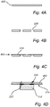
- Fig. 3 is a flow chart outlining steps of a method of manufacturing a smartcard 100 according to an embodiment of the invention and Figs. 4A-D illustrate selected steps of the method.
- Figs. 4A-D highlight the steps related to the contact formation between the antenna and the contact pads of the fingerprint sensor module 100.
- the general steps of forming a smartcard using various plastic foils and hot lamination can be assumed to be well known to the skilled person and will therefore not be detailed herein.
- a fingerprint sensor module 102 comprising contact pads 220 for contacting an antenna is provided 300, followed by providing 302 an antenna carrier layer 400 illustrated in Fig. 4A .
- openings 226 are formed 304 in the antenna carrier layer 400 in locations corresponding to the contact pads 220 of the fingerprint sensor module as illustrated in Fig. 4B .
- Fig. 4C illustrates forming 306 the conductive antenna 218 on the antenna carrier layer to form a complete antenna film 402.
- the conductive antenna comprises a copper wire being arranged on the antenna carrier according to a predetermined pattern, e.g. from a CAD template.
- the antenna 218, i.e. the copper wire, is embedded in an insulating coating in order to allow antenna crossings without short-circuiting the antenna.
- the antenna film 402 is completed with the patterned antenna, it is being flipped upside down and arranged 308 on the fingerprint sensor module 102 which is placed having the contact pads 220 facing upward as illustrated in Fig. 4D .
- the openings 226 are aligned with the contact pads 220 so that the antenna 218 is facing the contact pads 220 and also overlaps the contact pads 220.
- the conductive antenna 218 is contacted with a heated tool through the openings in the antenna carrier layer 400 in order to melt the insulating coating at the locations of the contact pads 220, thereby forming 312 an electrical contact between the conductive antenna 218 and the contact pads 220.
- the heating tool may for example be a hot welding tip or the like which can access the exposed antenna 218 through the opening 26.
- the antenna film and the fingerprint sensor module are embedded 314 in a smartcard through lamination.
- Lamination may be performed in the form of hot lamination where a stack of layers together forms a body of the smartcard 100.
- the lamination process may also comprise using a laminating plate having a protruding portion at a position corresponding to a location of the fingerprint sensor module.
- This will have the effect that an indentation 500 is formed in the smartcard surface at the location of a sensing area of the fingerprint sensor module 102 as illustrated in Fig. 5 .
- the indentation is advantageous in that it will guide the user to a correct finger placement on the smartcard. Moreover, the indentation will act to protect the outer surface of the smartcard from scratches and the like at the location of the sensor.
- Fig. 6 schematically illustrate an example embodiment of a portion of a smartcard 100 where the fingerprint sensor module 600 comprises wings 602, making the cross section of the fingerprint sensor module 600 T-shaped, here seen as an upside-down T.
- the contact pads 220 for connecting to the antenna 218 are located on a backside of the sensor module same as in the previously described embodiments. Accordingly, the described configuration of a smartcard is applicable for different designs of the fingerprint sensor module.
- Fig. 7 schematically illustrate an example embodiment of a portion of a smartcard 100 where the fingerprint sensor module 700 again comprises wings 702, but where the contact pads 704 are located on a top side of the wings 702 such that the contact pads 704 face in the same direction as a sensing surface 224 of the fingerprint sensor module 700.
- the illustrated embodiment may be advantageous in implementations where it is desirable to place the sensor with the sensing side up during the welding step, and/or if it is desirable to have the antenna closer to the surface of the card.
- the contact pads of the fingerprint sensor module on the side of the module, either directly on the side of the module or on the side of wings of a T-shaped module.
- Side facing contact pads can for example be made using a so-called castellation process.
- the fingerprint sensor module is described as a single module.
- the module may comprise additional components such as a secure element (SE) and/or one or more additional active or passive components, such as a processing unit.
- SE secure element
- additional active or passive components such as a processing unit.
Landscapes
- Engineering & Computer Science (AREA)
- Microelectronics & Electronic Packaging (AREA)
- Computer Hardware Design (AREA)
- Physics & Mathematics (AREA)
- General Physics & Mathematics (AREA)
- Theoretical Computer Science (AREA)
- Automation & Control Theory (AREA)
- Computer Security & Cryptography (AREA)
- General Engineering & Computer Science (AREA)
- Measurement Of The Respiration, Hearing Ability, Form, And Blood Characteristics Of Living Organisms (AREA)
- Image Input (AREA)
- Measurement Of Length, Angles, Or The Like Using Electric Or Magnetic Means (AREA)
Priority Applications (1)
| Application Number | Priority Date | Filing Date | Title |
|---|---|---|---|
| EP22201596.8A EP4137995B1 (de) | 2020-11-06 | 2021-10-29 | Chipkarte mit einem integrierten biometrischen sensormodul |
Applications Claiming Priority (1)
| Application Number | Priority Date | Filing Date | Title |
|---|---|---|---|
| SE2051294A SE2051294A1 (en) | 2020-11-06 | 2020-11-06 | Integrated biometric sensor module and method for manufacturing a smartcard comprising an integrated biometric sensor module |
Related Child Applications (3)
| Application Number | Title | Priority Date | Filing Date |
|---|---|---|---|
| EP22201596.8A Division EP4137995B1 (de) | 2020-11-06 | 2021-10-29 | Chipkarte mit einem integrierten biometrischen sensormodul |
| EP22201596.8A Previously-Filed-Application EP4137995B1 (de) | 2020-11-06 | 2021-10-29 | Chipkarte mit einem integrierten biometrischen sensormodul |
| EP22201596.8A Division-Into EP4137995B1 (de) | 2020-11-06 | 2021-10-29 | Chipkarte mit einem integrierten biometrischen sensormodul |
Publications (3)
| Publication Number | Publication Date |
|---|---|
| EP3995994A2 true EP3995994A2 (de) | 2022-05-11 |
| EP3995994A3 EP3995994A3 (de) | 2022-06-08 |
| EP3995994B1 EP3995994B1 (de) | 2023-01-18 |
Family
ID=78528659
Family Applications (2)
| Application Number | Title | Priority Date | Filing Date |
|---|---|---|---|
| EP22201596.8A Active EP4137995B1 (de) | 2020-11-06 | 2021-10-29 | Chipkarte mit einem integrierten biometrischen sensormodul |
| EP21205477.9A Active EP3995994B1 (de) | 2020-11-06 | 2021-10-29 | Integriertes biometrisches sensormodul und verfahren zur herstellung einer chipkarte mit einem integrierten biometrischen sensormodul |
Family Applications Before (1)
| Application Number | Title | Priority Date | Filing Date |
|---|---|---|---|
| EP22201596.8A Active EP4137995B1 (de) | 2020-11-06 | 2021-10-29 | Chipkarte mit einem integrierten biometrischen sensormodul |
Country Status (5)
| Country | Link |
|---|---|
| US (1) | US12197985B2 (de) |
| EP (2) | EP4137995B1 (de) |
| CN (1) | CN115039107A (de) |
| SE (1) | SE2051294A1 (de) |
| WO (1) | WO2022098276A1 (de) |
Families Citing this family (3)
| Publication number | Priority date | Publication date | Assignee | Title |
|---|---|---|---|---|
| US20240161534A1 (en) * | 2021-03-23 | 2024-05-16 | Fingerprint Cards Anacatum Ip Ab | Fingerprint sensor module and method for manufacturing a fingerprint sensor module |
| TWI793030B (zh) * | 2022-06-02 | 2023-02-11 | 義隆電子股份有限公司 | 具有指紋感測器的卡片及其製造方法 |
| DE102023120408B4 (de) * | 2023-08-01 | 2025-02-20 | Infineon Technologies Ag | Verfahren zum Herstellen eines Chipkarteninlays, Chipkarteninlay und Chipkarte |
Citations (1)
| Publication number | Priority date | Publication date | Assignee | Title |
|---|---|---|---|---|
| EP3123395A1 (de) | 2014-03-24 | 2017-02-01 | Fingerprint Cards AB | Kapazitiver fingerabdruckfühler mit verbessertem sensorelement |
Family Cites Families (21)
| Publication number | Priority date | Publication date | Assignee | Title |
|---|---|---|---|---|
| US20050129685A1 (en) * | 2003-09-18 | 2005-06-16 | Jingtai Cao | Use of IL-1 blockers to prevent corneal inflammation and neovascularization |
| KR20070051324A (ko) * | 2004-09-16 | 2007-05-17 | 서크 코퍼레이션 | 터치패드와 일체형으로 구현되는 비접촉 카드 판독기 |
| DE102010028926A1 (de) * | 2010-05-12 | 2011-11-17 | Bundesdruckerei Gmbh | Dokument und Verfahren zur Herstellung eines Dokuments |
| MY189207A (en) | 2012-07-12 | 2022-01-31 | Assa Abloy Ab | Method of manufacturing a functional inlay |
| US9704012B2 (en) * | 2015-09-10 | 2017-07-11 | Cypress Semiconductor Corporation | Fingerprint sensor pattern |
| EP3159832B1 (de) * | 2015-10-23 | 2020-08-05 | Nxp B.V. | Authentifizierungstoken |
| GB2548639A (en) * | 2016-03-24 | 2017-09-27 | Zwipe As | Method of manufacturing a smartcard |
| US9773153B1 (en) * | 2016-03-24 | 2017-09-26 | Fingerprint Cards Ab | Fingerprint sensor module |
| GB2552131A (en) * | 2016-05-06 | 2018-01-17 | Zwipe As | Electrical validation of a purported finger |
| GB201609572D0 (en) * | 2016-06-01 | 2016-07-13 | Zwipe As | Smartcard and method for controlling a smartcard |
| US10395164B2 (en) * | 2016-12-15 | 2019-08-27 | Fingerprint Cards Ab | Fingerprint sensing module and method for manufacturing the fingerprint sensing module |
| FR3063555B1 (fr) * | 2017-03-03 | 2021-07-09 | Linxens Holding | Carte a puce et procede de fabrication d’une carte a puce |
| US10282651B2 (en) * | 2017-03-23 | 2019-05-07 | Idex Asa | Sensor array system selectively configurable as a fingerprint sensor or data entry device |
| SE1750836A1 (en) * | 2017-06-28 | 2018-12-29 | Fingerprint Cards Ab | Fingerprint sensor module comprising antenna and method for manufacturing a fingerprint sensor module |
| US10445636B2 (en) * | 2017-07-03 | 2019-10-15 | Giesecke+Devrient Mobile Security Gmbh | Interference-optimised metal data carrier |
| FR3069081B1 (fr) | 2017-07-17 | 2021-08-20 | Safran Identity & Security | Carte electronique comprenant un capteur d'empreinte et procede de fabrication d'une telle carte |
| EP3802049B1 (de) | 2018-06-07 | 2023-04-19 | Fingerprint Cards Anacatum IP AB | Chipkarte mit einem fingerabdrucksensor und verfahren zur herstellung der chipkarte |
| US11126995B2 (en) * | 2018-08-13 | 2021-09-21 | Pierre T. Gandolfo | Radio frequency-based self-enrolment and data exchange methods for biometric smart cards and non-self-powered authentication devices |
| US12271455B2 (en) * | 2018-11-30 | 2025-04-08 | Rb Global Mobile Solutions, Llc | Digital identity management device |
| GB201909374D0 (en) * | 2019-06-28 | 2019-08-14 | Drayson Tech Europe Ltd | Impedance matching in near-field RF communication devices |
| DE102019128464A1 (de) * | 2019-10-22 | 2021-04-22 | Infineon Technologies Ag | Sensoreinrichtung, Verfahren zum Bilden einer Sensoreinrichtung, Chipkarte und Verfahren zum Bilden einer Chipkarte |
-
2020
- 2020-11-06 SE SE2051294A patent/SE2051294A1/en not_active Application Discontinuation
-
2021
- 2021-10-29 EP EP22201596.8A patent/EP4137995B1/de active Active
- 2021-10-29 CN CN202180012436.0A patent/CN115039107A/zh active Pending
- 2021-10-29 US US18/246,347 patent/US12197985B2/en active Active
- 2021-10-29 EP EP21205477.9A patent/EP3995994B1/de active Active
- 2021-10-29 WO PCT/SE2021/051085 patent/WO2022098276A1/en not_active Ceased
Patent Citations (1)
| Publication number | Priority date | Publication date | Assignee | Title |
|---|---|---|---|---|
| EP3123395A1 (de) | 2014-03-24 | 2017-02-01 | Fingerprint Cards AB | Kapazitiver fingerabdruckfühler mit verbessertem sensorelement |
Also Published As
| Publication number | Publication date |
|---|---|
| US12197985B2 (en) | 2025-01-14 |
| US20230359853A1 (en) | 2023-11-09 |
| EP4137995A1 (de) | 2023-02-22 |
| CN115039107A (zh) | 2022-09-09 |
| WO2022098276A1 (en) | 2022-05-12 |
| EP4137995B1 (de) | 2024-09-25 |
| EP3995994B1 (de) | 2023-01-18 |
| SE2051294A1 (en) | 2022-05-07 |
| EP3995994A3 (de) | 2022-06-08 |
Similar Documents
| Publication | Publication Date | Title |
|---|---|---|
| CN107229897B (zh) | 指纹传感器模块 | |
| CN108229340B (zh) | 指纹感测模块及其制造方法、智能卡及其制造方法 | |
| US12197985B2 (en) | Integrated biometric sensor module and method for manufacturing a smartcard comprising an integrated biometric sensor module | |
| AU2020371649B2 (en) | Metal card with biometric features | |
| US9633301B2 (en) | IC module, dual IC card, and method for manufacturing IC module | |
| CN109271835B (zh) | 具有指纹采集器的电子板及其制造方法 | |
| CN110392894A (zh) | 芯片卡和用于制造芯片卡的方法 | |
| EP3933697B1 (de) | Biometrisches bildgebungsmodul und verfahren zur herstellung eines biometrischen bildgebungsmoduls | |
| EP3836010B1 (de) | Biometrisches sensormodul zur integration in eine karte | |
| EP4281900B1 (de) | Fingerabdrucksensormodul für eine chipkarte und verfahren zur fingerabdruckerkennung in einer chipkarte | |
| JP2021018516A (ja) | Icモジュール、デュアルicカードおよびicモジュールの製造方法 | |
| JP2018092482A (ja) | Icモジュール、icモジュールを搭載した媒体およびicモジュールの製造方法 | |
| WO2024191337A1 (en) | Smartcard comprising fingerprint sensing device and manufacturing method thereof |
Legal Events
| Date | Code | Title | Description |
|---|---|---|---|
| PUAI | Public reference made under article 153(3) epc to a published international application that has entered the european phase |
Free format text: ORIGINAL CODE: 0009012 |
|
| STAA | Information on the status of an ep patent application or granted ep patent |
Free format text: STATUS: THE APPLICATION HAS BEEN PUBLISHED |
|
| PUAL | Search report despatched |
Free format text: ORIGINAL CODE: 0009013 |
|
| AK | Designated contracting states |
Kind code of ref document: A2 Designated state(s): AL AT BE BG CH CY CZ DE DK EE ES FI FR GB GR HR HU IE IS IT LI LT LU LV MC MK MT NL NO PL PT RO RS SE SI SK SM TR |
|
| AK | Designated contracting states |
Kind code of ref document: A3 Designated state(s): AL AT BE BG CH CY CZ DE DK EE ES FI FR GB GR HR HU IE IS IT LI LT LU LV MC MK MT NL NO PL PT RO RS SE SI SK SM TR |
|
| RIC1 | Information provided on ipc code assigned before grant |
Ipc: G06K 19/077 20060101ALI20220429BHEP Ipc: G06K 19/07 20060101AFI20220429BHEP |
|
| STAA | Information on the status of an ep patent application or granted ep patent |
Free format text: STATUS: REQUEST FOR EXAMINATION WAS MADE |
|
| 17P | Request for examination filed |
Effective date: 20220614 |
|
| RBV | Designated contracting states (corrected) |
Designated state(s): AL AT BE BG CH CY CZ DE DK EE ES FI FR GB GR HR HU IE IS IT LI LT LU LV MC MK MT NL NO PL PT RO RS SE SI SK SM TR |
|
| GRAP | Despatch of communication of intention to grant a patent |
Free format text: ORIGINAL CODE: EPIDOSNIGR1 |
|
| STAA | Information on the status of an ep patent application or granted ep patent |
Free format text: STATUS: GRANT OF PATENT IS INTENDED |
|
| INTG | Intention to grant announced |
Effective date: 20220823 |
|
| GRAS | Grant fee paid |
Free format text: ORIGINAL CODE: EPIDOSNIGR3 |
|
| GRAA | (expected) grant |
Free format text: ORIGINAL CODE: 0009210 |
|
| STAA | Information on the status of an ep patent application or granted ep patent |
Free format text: STATUS: THE PATENT HAS BEEN GRANTED |
|
| AK | Designated contracting states |
Kind code of ref document: B1 Designated state(s): AL AT BE BG CH CY CZ DE DK EE ES FI FR GB GR HR HU IE IS IT LI LT LU LV MC MK MT NL NO PL PT RO RS SE SI SK SM TR |
|
| REG | Reference to a national code |
Ref country code: GB Ref legal event code: FG4D |
|
| REG | Reference to a national code |
Ref country code: DE Ref legal event code: R096 Ref document number: 602021001269 Country of ref document: DE |
|
| REG | Reference to a national code |
Ref country code: CH Ref legal event code: EP |
|
| REG | Reference to a national code |
Ref country code: AT Ref legal event code: REF Ref document number: 1545095 Country of ref document: AT Kind code of ref document: T Effective date: 20230215 Ref country code: IE Ref legal event code: FG4D |
|
| REG | Reference to a national code |
Ref country code: LT Ref legal event code: MG9D |
|
| REG | Reference to a national code |
Ref country code: NL Ref legal event code: MP Effective date: 20230118 |
|
| REG | Reference to a national code |
Ref country code: AT Ref legal event code: MK05 Ref document number: 1545095 Country of ref document: AT Kind code of ref document: T Effective date: 20230118 |
|
| PG25 | Lapsed in a contracting state [announced via postgrant information from national office to epo] |
Ref country code: NL Free format text: LAPSE BECAUSE OF FAILURE TO SUBMIT A TRANSLATION OF THE DESCRIPTION OR TO PAY THE FEE WITHIN THE PRESCRIBED TIME-LIMIT Effective date: 20230118 |
|
| PG25 | Lapsed in a contracting state [announced via postgrant information from national office to epo] |
Ref country code: RS Free format text: LAPSE BECAUSE OF FAILURE TO SUBMIT A TRANSLATION OF THE DESCRIPTION OR TO PAY THE FEE WITHIN THE PRESCRIBED TIME-LIMIT Effective date: 20230118 Ref country code: PT Free format text: LAPSE BECAUSE OF FAILURE TO SUBMIT A TRANSLATION OF THE DESCRIPTION OR TO PAY THE FEE WITHIN THE PRESCRIBED TIME-LIMIT Effective date: 20230518 Ref country code: NO Free format text: LAPSE BECAUSE OF FAILURE TO SUBMIT A TRANSLATION OF THE DESCRIPTION OR TO PAY THE FEE WITHIN THE PRESCRIBED TIME-LIMIT Effective date: 20230418 Ref country code: LV Free format text: LAPSE BECAUSE OF FAILURE TO SUBMIT A TRANSLATION OF THE DESCRIPTION OR TO PAY THE FEE WITHIN THE PRESCRIBED TIME-LIMIT Effective date: 20230118 Ref country code: LT Free format text: LAPSE BECAUSE OF FAILURE TO SUBMIT A TRANSLATION OF THE DESCRIPTION OR TO PAY THE FEE WITHIN THE PRESCRIBED TIME-LIMIT Effective date: 20230118 Ref country code: HR Free format text: LAPSE BECAUSE OF FAILURE TO SUBMIT A TRANSLATION OF THE DESCRIPTION OR TO PAY THE FEE WITHIN THE PRESCRIBED TIME-LIMIT Effective date: 20230118 Ref country code: ES Free format text: LAPSE BECAUSE OF FAILURE TO SUBMIT A TRANSLATION OF THE DESCRIPTION OR TO PAY THE FEE WITHIN THE PRESCRIBED TIME-LIMIT Effective date: 20230118 Ref country code: AT Free format text: LAPSE BECAUSE OF FAILURE TO SUBMIT A TRANSLATION OF THE DESCRIPTION OR TO PAY THE FEE WITHIN THE PRESCRIBED TIME-LIMIT Effective date: 20230118 |
|
| PG25 | Lapsed in a contracting state [announced via postgrant information from national office to epo] |
Ref country code: SE Free format text: LAPSE BECAUSE OF FAILURE TO SUBMIT A TRANSLATION OF THE DESCRIPTION OR TO PAY THE FEE WITHIN THE PRESCRIBED TIME-LIMIT Effective date: 20230118 Ref country code: PL Free format text: LAPSE BECAUSE OF FAILURE TO SUBMIT A TRANSLATION OF THE DESCRIPTION OR TO PAY THE FEE WITHIN THE PRESCRIBED TIME-LIMIT Effective date: 20230118 Ref country code: IS Free format text: LAPSE BECAUSE OF FAILURE TO SUBMIT A TRANSLATION OF THE DESCRIPTION OR TO PAY THE FEE WITHIN THE PRESCRIBED TIME-LIMIT Effective date: 20230518 Ref country code: GR Free format text: LAPSE BECAUSE OF FAILURE TO SUBMIT A TRANSLATION OF THE DESCRIPTION OR TO PAY THE FEE WITHIN THE PRESCRIBED TIME-LIMIT Effective date: 20230419 Ref country code: FI Free format text: LAPSE BECAUSE OF FAILURE TO SUBMIT A TRANSLATION OF THE DESCRIPTION OR TO PAY THE FEE WITHIN THE PRESCRIBED TIME-LIMIT Effective date: 20230118 |
|
| REG | Reference to a national code |
Ref country code: DE Ref legal event code: R097 Ref document number: 602021001269 Country of ref document: DE |
|
| PG25 | Lapsed in a contracting state [announced via postgrant information from national office to epo] |
Ref country code: SM Free format text: LAPSE BECAUSE OF FAILURE TO SUBMIT A TRANSLATION OF THE DESCRIPTION OR TO PAY THE FEE WITHIN THE PRESCRIBED TIME-LIMIT Effective date: 20230118 Ref country code: RO Free format text: LAPSE BECAUSE OF FAILURE TO SUBMIT A TRANSLATION OF THE DESCRIPTION OR TO PAY THE FEE WITHIN THE PRESCRIBED TIME-LIMIT Effective date: 20230118 Ref country code: EE Free format text: LAPSE BECAUSE OF FAILURE TO SUBMIT A TRANSLATION OF THE DESCRIPTION OR TO PAY THE FEE WITHIN THE PRESCRIBED TIME-LIMIT Effective date: 20230118 Ref country code: DK Free format text: LAPSE BECAUSE OF FAILURE TO SUBMIT A TRANSLATION OF THE DESCRIPTION OR TO PAY THE FEE WITHIN THE PRESCRIBED TIME-LIMIT Effective date: 20230118 Ref country code: CZ Free format text: LAPSE BECAUSE OF FAILURE TO SUBMIT A TRANSLATION OF THE DESCRIPTION OR TO PAY THE FEE WITHIN THE PRESCRIBED TIME-LIMIT Effective date: 20230118 |
|
| PLBE | No opposition filed within time limit |
Free format text: ORIGINAL CODE: 0009261 |
|
| STAA | Information on the status of an ep patent application or granted ep patent |
Free format text: STATUS: NO OPPOSITION FILED WITHIN TIME LIMIT |
|
| PG25 | Lapsed in a contracting state [announced via postgrant information from national office to epo] |
Ref country code: SK Free format text: LAPSE BECAUSE OF FAILURE TO SUBMIT A TRANSLATION OF THE DESCRIPTION OR TO PAY THE FEE WITHIN THE PRESCRIBED TIME-LIMIT Effective date: 20230118 |
|
| 26N | No opposition filed |
Effective date: 20231019 |
|
| PG25 | Lapsed in a contracting state [announced via postgrant information from national office to epo] |
Ref country code: SI Free format text: LAPSE BECAUSE OF FAILURE TO SUBMIT A TRANSLATION OF THE DESCRIPTION OR TO PAY THE FEE WITHIN THE PRESCRIBED TIME-LIMIT Effective date: 20230118 |
|
| PG25 | Lapsed in a contracting state [announced via postgrant information from national office to epo] |
Ref country code: IT Free format text: LAPSE BECAUSE OF FAILURE TO SUBMIT A TRANSLATION OF THE DESCRIPTION OR TO PAY THE FEE WITHIN THE PRESCRIBED TIME-LIMIT Effective date: 20230118 Ref country code: MC Free format text: LAPSE BECAUSE OF FAILURE TO SUBMIT A TRANSLATION OF THE DESCRIPTION OR TO PAY THE FEE WITHIN THE PRESCRIBED TIME-LIMIT Effective date: 20230118 |
|
| REG | Reference to a national code |
Ref country code: BE Ref legal event code: MM Effective date: 20231031 |
|
| PG25 | Lapsed in a contracting state [announced via postgrant information from national office to epo] |
Ref country code: LU Free format text: LAPSE BECAUSE OF NON-PAYMENT OF DUE FEES Effective date: 20231029 |
|
| PG25 | Lapsed in a contracting state [announced via postgrant information from national office to epo] |
Ref country code: LU Free format text: LAPSE BECAUSE OF NON-PAYMENT OF DUE FEES Effective date: 20231029 |
|
| PG25 | Lapsed in a contracting state [announced via postgrant information from national office to epo] |
Ref country code: BE Free format text: LAPSE BECAUSE OF NON-PAYMENT OF DUE FEES Effective date: 20231031 |
|
| PG25 | Lapsed in a contracting state [announced via postgrant information from national office to epo] |
Ref country code: IE Free format text: LAPSE BECAUSE OF NON-PAYMENT OF DUE FEES Effective date: 20231029 |
|
| PG25 | Lapsed in a contracting state [announced via postgrant information from national office to epo] |
Ref country code: IE Free format text: LAPSE BECAUSE OF NON-PAYMENT OF DUE FEES Effective date: 20231029 |
|
| PG25 | Lapsed in a contracting state [announced via postgrant information from national office to epo] |
Ref country code: BG Free format text: LAPSE BECAUSE OF FAILURE TO SUBMIT A TRANSLATION OF THE DESCRIPTION OR TO PAY THE FEE WITHIN THE PRESCRIBED TIME-LIMIT Effective date: 20230118 |
|
| PG25 | Lapsed in a contracting state [announced via postgrant information from national office to epo] |
Ref country code: BG Free format text: LAPSE BECAUSE OF FAILURE TO SUBMIT A TRANSLATION OF THE DESCRIPTION OR TO PAY THE FEE WITHIN THE PRESCRIBED TIME-LIMIT Effective date: 20230118 |
|
| REG | Reference to a national code |
Ref country code: CH Ref legal event code: PL |
|
| PG25 | Lapsed in a contracting state [announced via postgrant information from national office to epo] |
Ref country code: CH Free format text: LAPSE BECAUSE OF NON-PAYMENT OF DUE FEES Effective date: 20241031 |
|
| PG25 | Lapsed in a contracting state [announced via postgrant information from national office to epo] |
Ref country code: CY Free format text: LAPSE BECAUSE OF FAILURE TO SUBMIT A TRANSLATION OF THE DESCRIPTION OR TO PAY THE FEE WITHIN THE PRESCRIBED TIME-LIMIT; INVALID AB INITIO Effective date: 20211029 |
|
| PG25 | Lapsed in a contracting state [announced via postgrant information from national office to epo] |
Ref country code: TR Free format text: LAPSE BECAUSE OF FAILURE TO SUBMIT A TRANSLATION OF THE DESCRIPTION OR TO PAY THE FEE WITHIN THE PRESCRIBED TIME-LIMIT Effective date: 20230118 |
|
| PGFP | Annual fee paid to national office [announced via postgrant information from national office to epo] |
Ref country code: DE Payment date: 20251029 Year of fee payment: 5 |
|
| PGFP | Annual fee paid to national office [announced via postgrant information from national office to epo] |
Ref country code: GB Payment date: 20251027 Year of fee payment: 5 |
|
| PGFP | Annual fee paid to national office [announced via postgrant information from national office to epo] |
Ref country code: FR Payment date: 20251027 Year of fee payment: 5 |
|
| PG25 | Lapsed in a contracting state [announced via postgrant information from national office to epo] |
Ref country code: HU Free format text: LAPSE BECAUSE OF FAILURE TO SUBMIT A TRANSLATION OF THE DESCRIPTION OR TO PAY THE FEE WITHIN THE PRESCRIBED TIME-LIMIT; INVALID AB INITIO Effective date: 20211029 |