EP3996476A1 - Coque de boîtier pour un boîtier accueillant une carte de circuit électrique et un ensemble avec un boîtier et une telle coque de bîtier - Google Patents
Coque de boîtier pour un boîtier accueillant une carte de circuit électrique et un ensemble avec un boîtier et une telle coque de bîtier Download PDFInfo
- Publication number
- EP3996476A1 EP3996476A1 EP20465584.9A EP20465584A EP3996476A1 EP 3996476 A1 EP3996476 A1 EP 3996476A1 EP 20465584 A EP20465584 A EP 20465584A EP 3996476 A1 EP3996476 A1 EP 3996476A1
- Authority
- EP
- European Patent Office
- Prior art keywords
- housing
- retaining ribs
- circuit board
- printed circuit
- side wall
- Prior art date
- Legal status (The legal status is an assumption and is not a legal conclusion. Google has not performed a legal analysis and makes no representation as to the accuracy of the status listed.)
- Withdrawn
Links
Images

Classifications
-
- H—ELECTRICITY
- H05—ELECTRIC TECHNIQUES NOT OTHERWISE PROVIDED FOR
- H05K—PRINTED CIRCUITS; CASINGS OR CONSTRUCTIONAL DETAILS OF ELECTRIC APPARATUS; MANUFACTURE OF ASSEMBLAGES OF ELECTRICAL COMPONENTS
- H05K5/00—Casings, cabinets or drawers for electric apparatus
- H05K5/0026—Casings, cabinets or drawers for electric apparatus provided with connectors and printed circuit boards [PCB], e.g. automotive electronic control units
- H05K5/0047—Casings, cabinets or drawers for electric apparatus provided with connectors and printed circuit boards [PCB], e.g. automotive electronic control units having a two-part housing enclosing a PCB
- H05K5/006—Casings, cabinets or drawers for electric apparatus provided with connectors and printed circuit boards [PCB], e.g. automotive electronic control units having a two-part housing enclosing a PCB characterized by features for holding the PCB within the housing
-
- H—ELECTRICITY
- H05—ELECTRIC TECHNIQUES NOT OTHERWISE PROVIDED FOR
- H05K—PRINTED CIRCUITS; CASINGS OR CONSTRUCTIONAL DETAILS OF ELECTRIC APPARATUS; MANUFACTURE OF ASSEMBLAGES OF ELECTRICAL COMPONENTS
- H05K7/00—Constructional details common to different types of electric apparatus
- H05K7/14—Mounting supporting structure in casing or on frame or rack
- H05K7/1417—Mounting supporting structure in casing or on frame or rack having securing means for mounting boards, plates or wiring boards
Definitions
- the invention relates to a housing shell for a housing for accommodating an electrical circuit board according to the preamble of claim 1.
- Housings for accommodating an electrical printed circuit board usually consist of two housing halves, with a printed circuit board being arranged between them and the housing halves and the printed circuit board lying between them being fastened by suitable fastening means, such as screws, at fastening points.
- At least one half of the housing is designed as a housing shell.
- the housing shell has a housing base and side walls arranged perpendicular thereto and at least one housing opening for inserting the printed circuit board.
- the housing In the corners of the side walls, there are fastening points projecting from the bottom of the housing, the predetermined height of which is less than the height of the side walls. At least the electrical printed circuit board can be fastened to these fastening points at this height parallel to the housing base or is fastened in the assembled state.
- the other half of the housing is preferably also fastened at the same time.
- these holding ribs are usually provided with a width or thickness which is many times greater than the width or thickness of the side walls. In the case of a thermal production of such a housing shell, however, such large retaining ribs can lead to tension in the housing shell itself.
- Circumferential retaining edges are also known, which have the disadvantage that they require a corresponding amount of material and their surface often cannot be manufactured so exactly parallel to the housing base that the printed circuit board always rests exactly at all points.
- the object of the invention is therefore to present a particularly suitable embodiment of a housing shell which, on the one hand, has low material and production costs and, on the other hand, sufficiently holds the printed circuit board and protects it from vibrations.
- a generic housing shell for a housing for accommodating an electrical printed circuit board consists of a housing base and side walls arranged perpendicular thereto, preferably on at least three of the sides, with the area for a plug connection also being provided instead of the fourth side wall, for example, or this side also being provided with a side wall can be.
- At least one housing opening is provided for inserting the printed circuit board, which can be arranged opposite the housing base or, for example, also on that side which is then closed by the plug connection.
- the housing opening can be closed by a simple cover, a plastic effusion or by another housing shell shaped according to the invention.
- Fastening points are provided in the corners of the housing shell near the side walls, which extend from the bottom of the housing to a predetermined height that is smaller than the height of the side walls and to which at least the electrical printed circuit board can be fastened at this height of the fastening points parallel to the bottom of the housing when installed of the housing is thus fixed.
- a plurality, ie at least two, of additional retaining ribs are provided at least on the longest side wall of the housing, but preferably on all existing side walls.
- the retaining ribs are arranged at right angles to this side wall and at right angles to the bottom of the housing and are designed with a height corresponding to the height of the fastening points, so that the printed circuit board is held in a plane parallel to the bottom of the housing via the fastening points and additional retaining ribs.
- the fastening points are each arranged at a distance from one another and project into the interior of the housing by a predetermined length parallel to the housing base.
- the invention provides that the retaining ribs each only have a thickness which deviates by at most 15% from the thickness of the side walls.
- at least two of these retaining ribs each form a common group of retaining ribs which are only spaced apart from one another by a distance which deviates at most 15% from the thickness of the retaining ribs.
- the deviation of +/-15% already represents a limit which already accepts certain disadvantages in the intended applications and every reduction in the deviations leads to an improvement in the overall effect, therefore a tolerance of only 5% is preferably provided and is an optimum was determined when the width was approximately the same, whereby of course production-related tolerances always have to be taken into account.
- This group as a sequence of thin retaining ribs and small distances acts like a continuous surface for the circuit board in terms of vibration, i.e. like a single retaining rib with a thickness corresponding to the overall width of the group, but on the other hand it can be produced with significantly less material and is easier to manufacture.
- this group of retaining ribs as a sequence of thin retaining ribs and small, approximately identically wide distances does not extend completely over the side walls but only within a group and points this group of retaining ribs to the attachment points and other groups if there are other groups on this side wall a spacing which is at least twice the spacing of the retaining ribs within a common group.
- the distance between the groups and also from the fastening points is preferably even significantly greater than twice, in particular more than ten times, the distance between the retaining ribs within the group.
- the one or the plurality of groups of retaining ribs is preferably arranged mirror-symmetrically to the center of the side wall between the attachment points. So if only a single group of retaining ribs is provided on a side wall, this will be arranged in the middle in a mirror-symmetrical manner. The same applies to the middle group in the case of an odd number of groups. However, if an even number of groups is provided, they are spaced evenly from this center.
- a larger number of groups of retaining ribs are arranged on the longer side wall than on the shorter side wall, especially in the case of a housing shell with two side walls of unequal length, but then possibly fewer retaining ribs are provided within the groups.
- the fastening points themselves also each have an additional retaining rib at least in the interior of the housing in the direction parallel to the longest side wall, i.e. the fastening points are next to a usually round bearing surface around the opening in the fastening points and also on the same Height remaining lateral webs have as retaining ribs, which correspondingly increase the effective contact surface of the attachment points in the corresponding directions.
- the specific number of retaining ribs per group as well as the number of groups and thus implicitly the distance between the groups and the attachment points is application-specific at least depending on the parameters of the circuit board, for example the dimensions of the circuit board, its rigidity and the assembly of the circuit board definitely. This is preferably done by a vibration simulation of the housing with the attached and populated printed circuit board at at least one predetermined excitation frequency and the number of retaining ribs per group as well as the number of groups is determined in such a way that the vibration of the printed circuit board is at least smaller than a maximum permissible limit, preferably minimized is.
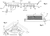
- FIG. 1 a housing shell 1 according to a particularly preferred embodiment of the invention, in which there is a complete side wall 12 on 3 of the sides starting from the housing base 10, while on the in 1 There is no complete side wall on the front side, but a recess into which the connector area on the circuit board is subsequently inserted.
- Retaining ribs 13 are arranged on the opposite side wall 12X, which extends in the X direction and is therefore the longest, and also here, in the preferred embodiment, on the side walls 12Y adjacent thereto in the Y direction.
- Fastening points 11 are provided in the corners of the side walls 12 and extend from the bottom of the housing to a predetermined height Z11 that is smaller than the height Z12 of the side walls.
- the attachment points 11 have in a conventional manner an opening for the passage of a fastener, For example, a screw and a peripheral edge, the electric circuit board being fastened parallel to the housing base 10 at this height Z11 of the fastening points 11 on this edge.
- the retaining ribs 13 are arranged at right angles to the respective side wall (12X or 12Y) and at right angles to the housing base 10 .
- the retaining ribs 13 are arranged at a distance from one another and from the attachment points 11 and project parallel to the housing base 10 by a predetermined length into the interior of the housing. For the retaining ribs on the longest side wall 12 X this would be in the Y direction.
- the distances X are also significantly more than twice 15 and X16, more than ten times greater than the distance X14 between 2 adjacent retaining ribs within a group.
- the groups are each arranged mirror-symmetrically to the middle of the side wall between the attachment points 11, as shown in FIG figure 1 sketched in dashed lines at the positions with the distances X1/2 for the side wall 12X and at position Y1/2 for the side walls 12Y.
- the 2 groups GX.1 and GX.2 are also arranged mirror-symmetrically to the center X1/2 of the length X1 of the housing shell1.
- the groups GX.1, GX.2,GY of retaining ribs 13 act according to the invention approximately as one Supporting surface corresponding to the width of the entire group, although the retaining ribs 13 are each interrupted by the distances 14 from each other.
- two groups with 5 retaining ribs each on the long side 12X and one group each with 5 retaining ribs on the short side 12Y came out as the best solution from the simulation, but it should be made clear that a different number of Retaining ribs with other dimensions of the printed circuit board or their assembly is conceivable, e.g. on the long side also two groups with e.g the short side.
- the figure 2 shows another detailed view of the side wall 12 X with the 2 groups of retaining ribs, as these are already shown with regard to 1 was explained in detail.
- FIG 3 shows an enlargement of a special further development, which is also already in 1 shown, but has not yet been discussed in such detail as to how this is to be done.
- the fastening points 11 each have an additional holding rib 111 at least in the direction parallel to the longest side wall 12X, here even in both directions, ie also in the Y-direction. As a result, the bearing surface of the fastening point 11 acting on the printed circuit board increases again.
- the height in the Z-direction of the fastening point 11 itself and of its holding ribs 111 and of the holding ribs 13 is the same in relation to the housing base, so that the printed circuit board lies flat and parallel to the housing base.
- Fig.4 now outlines for the sake of completeness an electronic assembly with such a housing shell 1 according to the invention and a second housing shell 2 and a printed circuit board with a connector area 3 located thereon, which is on the here in the Fig.4 front housing wall is arranged.
- fastening points 21 are each aligned with the fastening points 11 and fastening means, not shown in detail, for example screws, can be provided there for closing the housing, which preferably also clamp the circuit board between them at the same time.
- the housing shell or the entire housing can be made of plastic or metal and the invention is suitable in both cases.
- metallic housings can also be electrically grounded via the housing, in which case, in addition to or instead of the contact via the attachment points, this can also be done via the retaining ribs and retaining ribs on both halves of the housing even have the effect of a Faraday cage be reinforced by the retaining ribs.
Landscapes
- Engineering & Computer Science (AREA)
- Microelectronics & Electronic Packaging (AREA)
- Casings For Electric Apparatus (AREA)
- Mounting Of Printed Circuit Boards And The Like (AREA)
Priority Applications (3)
| Application Number | Priority Date | Filing Date | Title |
|---|---|---|---|
| EP20465584.9A EP3996476A1 (fr) | 2020-11-05 | 2020-11-05 | Coque de boîtier pour un boîtier accueillant une carte de circuit électrique et un ensemble avec un boîtier et une telle coque de bîtier |
| PCT/DE2021/200149 WO2022096068A1 (fr) | 2020-11-05 | 2021-10-07 | Coque de boîtier pour un boîtier destiné à recevoir une carte de circuit électrique, et ensemble comportant un boîtier doté d'une telle coque de boîtier |
| DE112021005803.7T DE112021005803A5 (de) | 2020-11-05 | 2021-10-07 | Gehäuseschale für ein Gehäuse zur Aufnahme einer elektrischen Leiterplatte sowie Baugruppe mit einem Gehäuse mit einer solchen Gehäuseschale |
Applications Claiming Priority (1)
| Application Number | Priority Date | Filing Date | Title |
|---|---|---|---|
| EP20465584.9A EP3996476A1 (fr) | 2020-11-05 | 2020-11-05 | Coque de boîtier pour un boîtier accueillant une carte de circuit électrique et un ensemble avec un boîtier et une telle coque de bîtier |
Publications (1)
| Publication Number | Publication Date |
|---|---|
| EP3996476A1 true EP3996476A1 (fr) | 2022-05-11 |
Family
ID=73598040
Family Applications (1)
| Application Number | Title | Priority Date | Filing Date |
|---|---|---|---|
| EP20465584.9A Withdrawn EP3996476A1 (fr) | 2020-11-05 | 2020-11-05 | Coque de boîtier pour un boîtier accueillant une carte de circuit électrique et un ensemble avec un boîtier et une telle coque de bîtier |
Country Status (3)
| Country | Link |
|---|---|
| EP (1) | EP3996476A1 (fr) |
| DE (1) | DE112021005803A5 (fr) |
| WO (1) | WO2022096068A1 (fr) |
Citations (7)
| Publication number | Priority date | Publication date | Assignee | Title |
|---|---|---|---|---|
| DE4439471A1 (de) * | 1994-11-08 | 1996-05-09 | Telefunken Microelectron | Baugruppe |
| US20040120124A1 (en) * | 2002-12-18 | 2004-06-24 | Patrick Cauwels | Structure and method for positively locating components |
| DE102006006078A1 (de) * | 2006-02-09 | 2007-09-06 | Siemens Ag | Elektronische Steuerungseinheit, insbesondere zur Steuerung eines Sicherheitssystems und/oder Komfortsystems in einem Kraftfahrzeug |
| US20090295985A1 (en) * | 2008-05-30 | 2009-12-03 | Sony Corporation | Camera device |
| US20110075023A1 (en) * | 2009-09-25 | 2011-03-31 | Aisin Seiki Kabushiki Kaisha | Substrate holding apparatus |
| KR20120127041A (ko) * | 2011-05-13 | 2012-11-21 | 현대자동차주식회사 | 기판 유동 방지 구조를 구비한 전자회로기판 유닛 |
| DE102016120712A1 (de) * | 2016-10-28 | 2018-05-03 | Mimatic Gmbh | Gehäuse zur Aufnahme einer Platine, Funktionselement |
Family Cites Families (3)
| Publication number | Priority date | Publication date | Assignee | Title |
|---|---|---|---|---|
| US6144552A (en) * | 1999-04-26 | 2000-11-07 | Emc Corporation | Handheld computer system |
| JP3804657B2 (ja) * | 2003-01-08 | 2006-08-02 | ソニー株式会社 | 外部記憶装置 |
| US9195281B2 (en) * | 2013-12-31 | 2015-11-24 | Ultravision Technologies, Llc | System and method for a modular multi-panel display |
-
2020
- 2020-11-05 EP EP20465584.9A patent/EP3996476A1/fr not_active Withdrawn
-
2021
- 2021-10-07 DE DE112021005803.7T patent/DE112021005803A5/de active Pending
- 2021-10-07 WO PCT/DE2021/200149 patent/WO2022096068A1/fr not_active Ceased
Patent Citations (7)
| Publication number | Priority date | Publication date | Assignee | Title |
|---|---|---|---|---|
| DE4439471A1 (de) * | 1994-11-08 | 1996-05-09 | Telefunken Microelectron | Baugruppe |
| US20040120124A1 (en) * | 2002-12-18 | 2004-06-24 | Patrick Cauwels | Structure and method for positively locating components |
| DE102006006078A1 (de) * | 2006-02-09 | 2007-09-06 | Siemens Ag | Elektronische Steuerungseinheit, insbesondere zur Steuerung eines Sicherheitssystems und/oder Komfortsystems in einem Kraftfahrzeug |
| US20090295985A1 (en) * | 2008-05-30 | 2009-12-03 | Sony Corporation | Camera device |
| US20110075023A1 (en) * | 2009-09-25 | 2011-03-31 | Aisin Seiki Kabushiki Kaisha | Substrate holding apparatus |
| KR20120127041A (ko) * | 2011-05-13 | 2012-11-21 | 현대자동차주식회사 | 기판 유동 방지 구조를 구비한 전자회로기판 유닛 |
| DE102016120712A1 (de) * | 2016-10-28 | 2018-05-03 | Mimatic Gmbh | Gehäuse zur Aufnahme einer Platine, Funktionselement |
Also Published As
| Publication number | Publication date |
|---|---|
| WO2022096068A1 (fr) | 2022-05-12 |
| DE112021005803A5 (de) | 2023-08-24 |
Similar Documents
| Publication | Publication Date | Title |
|---|---|---|
| DE69120688T2 (de) | Mehrpoliger abgeschirmter verbinder mit gemeinsamer erdung | |
| EP3080874B1 (fr) | Cadre de retenue pour un connecteur par enfichage | |
| EP3217483A1 (fr) | Cadre de retenue pour connecteur à fiche | |
| DE102013113976A1 (de) | Halterahmen für einen Steckverbinder | |
| DE102013113975A1 (de) | Halterahmen für einen Steckverbinder | |
| DE102013215302A1 (de) | Flachkontakt für einen Stecker, Aufnahmeblock für einen Flachkontakt und Stecker | |
| DE102020211730B3 (de) | Gehäuse für eine auf einer Leiterplatte angeordneten elektronische Schaltung | |
| DE102016119061A1 (de) | Rangierwabe | |
| EP0447942A1 (fr) | Réglette enfichable pour une interconnexion imperméable à des rayonnements perturbateurs d'éléments de bord voisins métalliques | |
| DE102017217104A1 (de) | Haltestruktur für elektronische Komponente, elektrischer Anschlusskasten und Kabelbaum | |
| DE2507721B2 (de) | Selbsttragende Mosaikschaltwand | |
| EP0313131A2 (fr) | Dispositif de logement de cartes blindées | |
| EP3996476A1 (fr) | Coque de boîtier pour un boîtier accueillant une carte de circuit électrique et un ensemble avec un boîtier et une telle coque de bîtier | |
| EP0516986B1 (fr) | Rack électronique | |
| EP2831970B1 (fr) | Module système pour la technique d'installation électrique d'un bâtiment et la technique de communication de porte | |
| EP0596349A2 (fr) | Support pour installation électrique | |
| DE3915651C2 (fr) | ||
| DE102013113973B4 (de) | Metallischer Halterahmen für einen Steckverbinder sowie Verfahren zur Herstellung | |
| DE69904504T2 (de) | Busschienenverbindungsstruktur | |
| DE3200729C2 (de) | Einrichtung zur Befestigung von Leiterplatten in einem Trägerrahmen | |
| DE3624756C2 (fr) | ||
| DE102017207677A1 (de) | Platinenverbindungsstecker, Platinenverbund und Verfahren zur Herstellung eines Platinenverbindungssteckers | |
| DE2552362B2 (de) | Elektrisches Geräte-Steckbauteil | |
| DE102023107681A1 (de) | Steckverbindermodul für einen modularen Industriesteckverbinder | |
| DE69012554T2 (de) | Leiterplatte. |
Legal Events
| Date | Code | Title | Description |
|---|---|---|---|
| PUAI | Public reference made under article 153(3) epc to a published international application that has entered the european phase |
Free format text: ORIGINAL CODE: 0009012 |
|
| STAA | Information on the status of an ep patent application or granted ep patent |
Free format text: STATUS: THE APPLICATION HAS BEEN PUBLISHED |
|
| AK | Designated contracting states |
Kind code of ref document: A1 Designated state(s): AL AT BE BG CH CY CZ DE DK EE ES FI FR GB GR HR HU IE IS IT LI LT LU LV MC MK MT NL NO PL PT RO RS SE SI SK SM TR |
|
| RAP1 | Party data changed (applicant data changed or rights of an application transferred) |
Owner name: CONTINENTAL AUTOMOTIVE TECHNOLOGIES GMBH |
|
| STAA | Information on the status of an ep patent application or granted ep patent |
Free format text: STATUS: REQUEST FOR EXAMINATION WAS MADE |
|
| 17P | Request for examination filed |
Effective date: 20221111 |
|
| RBV | Designated contracting states (corrected) |
Designated state(s): AL AT BE BG CH CY CZ DE DK EE ES FI FR GB GR HR HU IE IS IT LI LT LU LV MC MK MT NL NO PL PT RO RS SE SI SK SM TR |
|
| RAP3 | Party data changed (applicant data changed or rights of an application transferred) |
Owner name: CONTINENTAL AUTOMOTIVE TECHNOLOGIES GMBH |
|
| STAA | Information on the status of an ep patent application or granted ep patent |
Free format text: STATUS: THE APPLICATION IS DEEMED TO BE WITHDRAWN |
|
| 18D | Application deemed to be withdrawn |
Effective date: 20240601 |