EP4001930A1 - Appareil de mesure - Google Patents
Appareil de mesure Download PDFInfo
- Publication number
- EP4001930A1 EP4001930A1 EP21208663.1A EP21208663A EP4001930A1 EP 4001930 A1 EP4001930 A1 EP 4001930A1 EP 21208663 A EP21208663 A EP 21208663A EP 4001930 A1 EP4001930 A1 EP 4001930A1
- Authority
- EP
- European Patent Office
- Prior art keywords
- current
- alternating
- signals
- capacitance
- detection
- Prior art date
- Legal status (The legal status is an assumption and is not a legal conclusion. Google has not performed a legal analysis and makes no representation as to the accuracy of the status listed.)
- Granted
Links
Images


Classifications
-
- G—PHYSICS
- G01—MEASURING; TESTING
- G01N—INVESTIGATING OR ANALYSING MATERIALS BY DETERMINING THEIR CHEMICAL OR PHYSICAL PROPERTIES
- G01N27/00—Investigating or analysing materials by the use of electric, electrochemical, or magnetic means
- G01N27/02—Investigating or analysing materials by the use of electric, electrochemical, or magnetic means by investigating impedance
- G01N27/22—Investigating or analysing materials by the use of electric, electrochemical, or magnetic means by investigating impedance by investigating capacitance
- G01N27/228—Circuits therefor
-
- G—PHYSICS
- G01—MEASURING; TESTING
- G01R—MEASURING ELECTRIC VARIABLES; MEASURING MAGNETIC VARIABLES
- G01R27/00—Arrangements for measuring resistance, reactance, impedance, or electric characteristics derived therefrom
- G01R27/02—Measuring real or complex resistance, reactance, impedance, or other two-pole characteristics derived therefrom, e.g. time constant
- G01R27/26—Measuring inductance or capacitance; Measuring quality factor, e.g. by using the resonance method; Measuring loss factor; Measuring dielectric constants ; Measuring impedance or related variables
- G01R27/2605—Measuring capacitance
-
- G—PHYSICS
- G01—MEASURING; TESTING
- G01R—MEASURING ELECTRIC VARIABLES; MEASURING MAGNETIC VARIABLES
- G01R31/00—Arrangements for testing electric properties; Arrangements for locating electric faults; Arrangements for electrical testing characterised by what is being tested not provided for elsewhere
- G01R31/50—Testing of electric apparatus, lines, cables or components for short-circuits, continuity, leakage current or incorrect line connections
- G01R31/64—Testing of capacitors
Definitions
- the present disclosure relates to a measuring apparatus and, for example, relates to a measuring apparatus that can measure the capacitance of a device under test by applying a voltage to the device and measuring a current through the device.
- Japanese Patent Laid-Open No. 2006-242718 describes an impedance detection device used for concurrently detecting the c component and the r component between the gate and the source of a transistor, and obtaining their values.
- the impedance detection device includes an alternating-current signal generation unit for applying an alternating-current signal to a detection target, a conversion unit that converts a current generated in accordance with the impedance of the detection target into a voltage, and a synchronous detection unit that performs synchronous detection on an output signal of the conversion unit to detect a first component that is one of the c component, the 1 component, and the r component of the detection target.
- Japanese Patent Laid-Open No. 2006-242718 describes that performing synchronous detection on an output signal, which has been obtained by subtracting the first component from the output signal of the conversion unit to reduce the first component, can accurately detect impedance.
- FIG. 5 illustrates a state in which the measuring apparatus is connected to a device 106 under test via the terminals 105 and 107.
- an alternating-current signal with a predetermined frequency generated by the signal source 101, the frequency divider 102, and the waveform shaping filter 103 is applied to the device 106 under test via the terminal 105.
- An output signal from the device 106 under test is obtained with the terminal 107, and then, synchronous detection is performed on the signal with the multiplier 110.
- the capacitance measuring instrument 112 detects the voltage value of the signal subjected to synchronous detection, thereby measuring the capacitance value of the device under test.
- the capacitance value is outside the range that has been conventionally supposed, it is considered that measurement accuracy would decrease both in the region where the capacitance value is small and the region where the capacitance value is large. Consequently, regarding the device 106 under test of the conventional measuring apparatus, if the capacitance values outside the range that has been conventionally supposed are included in the measurement target, detection sensitivity becomes nonuniform as illustrated in FIG. 8 . Therefore, if the range of capacitance values to be measured of the device under test is increased so as to allow the capacitance values outside the range that has been conventionally supposed to be included in the measurement target, measurement accuracy would decrease.
- the present disclosure is related to providing a measuring apparatus that can detect a wide range of capacitance values with high sensitivity.
- a measuring apparatus includes an alternating-current signal generation unit that generates N (where N is a natural number not less than 2) detection alternating-current signals with different frequencies, a superposition unit that superposes the N detection alternating-current signals, an output terminal that outputs to a device under test a detection alternating-current signal obtained through the superposition, an input terminal that receives a measurement alternating-current signal output from the device under test to which the detection alternating-current signal obtained through the superposition has been applied, a multiplication processor that multiplies the measurement alternating-current signal by the N detection alternating-current signals with different frequencies, thereby obtaining N synchronous detection signals, a low-pass filter processor that performs a low-pass filter process on the N synchronous detection signals, thereby obtaining N direct-current voltage signals, and a capacitance measuring unit that measures as the capacitance value of the device under test a capacitance value corresponding to the voltage values of the N direct-current voltage signals.
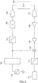
- FIG. 1 is a diagram illustrating the configuration of a measuring apparatus according to an embodiment.
- the measuring apparatus of the present embodiment measures the magnitude of the capacitance value of a device under test (DUT) 7 in a state in which an output terminal 6, which outputs a detection signal, and an input terminal 8, which inputs a signal from the device 7 under test to the measuring apparatus, are physically in contact with the device 7 under test. Based on the magnitude of the capacitance value measured by the measuring apparatus, it is possible to determine if the output terminal 6 and the input terminal 8 are electrically connected to the device 7 under test properly. For example, there may be a case where the two terminals 6 and 8 and the device 7 under test are not electrically or physically in contact with each other due to rust generated on the terminal portions of the device 7 under test, for example.
- the measuring apparatus includes, on the output side for the device 7 under test, a signal source 1, a frequency divider 2, two waveform shaping filters 3a and 3b, a multiplexer 4, an impedance adjustment circuit 5, and an output terminal 6.
- the measuring apparatus includes, on the input side from the device 7 under test, the input terminal 8, a current-voltage converter circuit 9, a brancher 10, two amplifiers 11a and 11b, two multipliers 12a and 12b, two low-pass filters 13a and 13b, a multiplexer 14, and a capacitance measuring unit 15.
- the signal source 1 and the frequency divider 2 can constitute the alternating-current signal generation unit.
- the signal source 1 is an oscillator that outputs an alternating-current signal with a specific frequency.
- Examples of the signal source 1 include, but are not limited to, a crystal oscillator that outputs an alternating-current signal with a frequency of 1 MHz as a specific frequency.
- the frequency divider 2 converts the alternating-current signal with a specific frequency output from the signal source 1 into a signal with a frequency suitable for measuring the device 7 under test.
- an analog divider circuit can be used.
- the frequency divider 2 can convert the frequency of the signal source into two different frequencies f1 and f2, for example. As the two different frequencies f1 and f2, frequencies are selected that allow the value of the parasitic capacitance of the device 7 under test to be measured to be included in the measurement range, and such frequencies are set in advance.
- the waveform shaping filters 3a and 3b are filters that shape the waveforms of the two alternating-current signals with different frequencies f1 and f2, which have been generated by the frequency divider 2, from rectangular waves into sine waves.
- band-limiting circuits can be used as the waveform shaping filters 3a and 3b. Changing the waveforms of the alternating-current signals into sine waves with the waveform shaping filters 3a and 3b can facilitate detection.
- the multiplexer (which is an example of a superposition unit) 4 multiplexes (superposes) the two alternating-current signals with different frequencies output from the two waveform shaping filters 3a and 3b into one alternating-current signal, and outputs the signal to the impedance adjustment circuit 5.
- an analog adding circuit can be used as the multiplexer 4.
- the impedance adjustment circuit 5 is a circuit that adjusts the output impedance of the alternating-current signal generated for detection so as to be able to output an alternating-current signal suited for the device 7 under test.
- a circuit obtained by connecting a resistive element or a capacitive element can be used, for example.
- the output terminal 6 is a signal output terminal connected to the input terminal of the device 7 under test.
- the output terminal 6 When the output terminal 6 is properly connected to the input terminal of the device 7 under test, the output terminal 6 outputs to the device 7 under test the alternating-current signal with the adjusted impedance as a detection alternating-current signal.
- the input terminal 8 is an input terminal connected to the output terminal of the device 7 under test. When the input terminal 8 is properly connected to the output terminal of the device 7 under test, the input terminal 8 receives a measurement alternating-current signal output from the device 7 under test to which the detection alternating-current signal has been applied.
- the current-voltage converter circuit 9 is a circuit that converts the current of the measurement alternating-current signal into a voltage. When the current-voltage converter circuit 9 convers the current into a voltage, the current of the measurement alternating-current signal can be detected as a voltage.
- the brancher 10 branches the measurement alternating-current signal output from the current-voltage converter circuit 9 into two signals, and then inputs one of the signals to the first amplifier 11a, and inputs another signal to the second amplifier 11b.
- Each of the two amplifiers 11a and 11b is an amplifier that amplifies a signal component with a predetermined frequency of the measurement alternating-current signal.
- the first amplifier 11a amplifies a signal component with the frequency f1 of the measurement alternating-current signal.
- the second amplifier 11b amplifies a signal component with the frequency f2 of the measurement alternating-current signal.
- the two multipliers 12a and 12b respectively multiply the measurement alternating-current signals with the signal components with the predetermined frequencies amplified by the two amplifiers 11a and 11b by the detection alternating-current signals with the corresponding frequencies f1 and f2, thereby obtaining two synchronous detection signals.
- the first multiplier 12a can obtain a synchronous detection signal by multiplying the measurement alternating-current signal with the amplified signal component with the frequency f1 by the detection alternating-current signal with the frequency f1.
- the second multiplier 12b can obtain another synchronous detection signal by multiplying the measurement alternating-current signal with the amplified signal component with the frequency f2 by the detection alternating-current signal with the frequency f2. That is, synchronous detection signals with two frequencies f1 and f2 can be obtained with the two multipliers 12a and 12b.
- the two low-pass filters (which are examples of low-pass filter processors) 13a and 13b are filters that respectively perform a low-pass filter process on the two synchronous detection signals, thereby obtaining two direct-current voltage signals.
- the low-pass filter process is a process of passing only frequency components of less than frequencies f1' and f2' corresponding to the frequencies f1 and f2 used for synchronous detection. With the two low-pass filters 13a and 13b, it is possible to remove alternating-current ripples and extract direct-current signal components needed for the measurement.
- the multiplexer 14 multiplexes the two direct-current voltage signals, and inputs the resulting signal to the capacitance measuring unit 15.
- an analog adding circuit can be used as the multiplexer 14.
- the capacitance measuring unit 15 measures as the capacitance value of the device 7 under test a capacitance value corresponding to the voltage value of the direct-current voltage signal received from the multiplexer 14.
- the capacitance measuring unit 15 can determine the capacitance value corresponding to the voltage value of the direct-current voltage signal, which has been obtained through multiplexing, based on the capacitance vs. detected voltage characteristics.
- the capacitance vs. detected voltage characteristics are represented by a fitting curve that is determined according to the characteristics (e.g., predetermined insulation resistance) of the device 7 under test estimated as a measurement target.
- the capacitance vs. detected voltage characteristics can be stored in a storage unit (not illustrated) of the measuring apparatus in advance. Although the capacitance vs. detected voltage characteristics may be stored in the storage unit of the measuring apparatus in advance before shipment from the factory, the capacitance vs. detected voltage characteristics may be updated at any point in time after shipment from the factory.
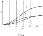
- FIG. 2 is a chart illustrating the capacitance vs. detected voltage characteristics used in the measuring apparatus of the embodiment. Specifically, FIG. 2 illustrates capacitance vs. detected voltage characteristics f t used in the measuring apparatus of the embodiment, capacitance vs. detected voltage characteristics f 1 at a first frequency f1, and capacitance vs. detected voltage characteristics f 2 at a second frequency f2.
- the capacitance vs. detected voltage characteristics f t used in the measuring apparatus of the present embodiment are characteristics obtained by superposing the capacitance vs. detected voltage characteristics f 1 and f 2 at the two frequencies f1 and f2.
- the two frequencies f1 and f2 are equal to the frequencies f1 and f2 of the detection alternating-current signals generated by the frequency divider 2.
- the capacitance measuring unit 15 can, upon detecting the voltage value of the signal obtained by adding together the two direct-current voltage signals, identify the capacitance value corresponding to the detected voltage value with reference to the capacitance vs. detected voltage characteristics ft, and thus determine the identified capacitance value as the measured value.
- the frequencies f1 and f2 used in the measuring apparatus of the present embodiment can be selected so as to allow desired capacitance values to be included in the region where the slope of the capacitance vs. detected voltage characteristics is steep. Further, as the frequencies f1 and f2, it is preferable to set frequencies at which high-sensitivity regions where the magnitude of fluctuation in the voltage value with respect to fluctuation in the capacitance value is greater than or equal to a predetermined value do not overlap with each other.
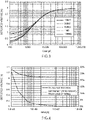
- FIG. 3 is a graph illustrating changes in the capacitance vs. detected voltage characteristics for each of different insulation resistance values in the configuration of the measuring apparatus of the embodiment. Specifically, FIG. 3 illustrates the capacitance vs. detected voltage characteristics when the insulation resistance value is 100 k ⁇ , 200 k ⁇ , 500 k ⁇ , 1 M ⁇ , and 100 M ⁇ . In the configuration of the measuring apparatus of the present embodiment, the difference among the capacitance vs. detected voltage characteristics depending on the insulation resistance value is also smaller in the low capacitance region as compared to that of the conventional measuring apparatus illustrated in FIG. 6 .
- FIG. 4 is a chart illustrating the influence of the insulation resistance value on the measured voltage in the configuration of the measuring apparatus of the embodiment. Specifically, FIG. 4 illustrates changes in the voltage detected when the capacitance value is 1 nF for each insulation resistance value, and the influence of the difference, expressed in percentage, between the voltage and the voltage detected when the insulation resistance value is 100 M ⁇ .
- the difference between the voltage detected when the capacitance value is 1 nF and the voltage detected when the insulation resistance is 100 M ⁇ is as small as 28% at a maximum. This is considered to not be an issue in practice as the influence of the insulation resistance is significantly smaller than that in the conventional measuring apparatus illustrated in FIG. 7 where the difference is 85% or more at a maximum.
- the influence of insulation resistance can be suppressed more than that in the conventional measuring apparatus.
- a wide range of capacitance values can be detected with high sensitivity.
- signals with different frequencies generated by the frequency divider 2 may be signals with two or more different frequencies.
- signals with different frequencies generated by the frequency divider 2 may be signals with two or more different frequencies.
- waveform shaping filters 3a and 3b as many amplifiers 11a and 11b, as many multipliers 12a and 12b, and as many low-pass filters 13a and 13b as the number of signals with different frequencies are provided.
- measurement is performed by converting the current of a measurement alternating-current signal into a voltage using the current-voltage converter circuit 9, but the present disclosure is not limited to such a configuration.
- the configuration including analog circuits in the aforementioned embodiment may be provided using digital circuits.
- an FPGA programmed to implement the functions of the brancher 10, the two amplifiers 11a and 11b, the two multipliers 12a and 12b, the two low-pass filters 13a and 13b, the multiplexer 14, and the capacitance measuring unit 15.
- a program processing unit for example, a microcontroller: MCU
- a processor such as a CPU
- various memories such as ROM and RAM
- hardware components such as a timer (i.e., a counter), an A/D converter circuit, an input-output I/F circuit, and a clock generation circuit that are connected via buses or dedicated wires.
- a timer i.e., a counter
- the configuration of each of the aforementioned functional units can be implemented as the processor of the program processing unit performs various arithmetic operations in accordance with programs stored in a flash memory 21 such as a memory, and peripheral circuits such as the A/D converter circuit and the input-output I/F circuit are controlled.
- N detection alternating-current signals are generated by dividing a signal output from the signal source 1 using the frequency divider 2, but the present disclosure is not limited to such a configuration.
- N signal sources may be used to generate N detection alternating-current signals.
- the capacitance measuring unit 15 detects the voltage value of a signal obtained by adding together two direct-current voltage signals, and determines a capacitance value corresponding to the detected voltage value based on the capacitance vs. detected voltage characteristics ft, but the present disclosure is not limited to such a configuration.
- the capacitance measuring unit 15 may detect the voltage values of the two direct-current voltage signals and measure as the capacitance value of the device 7 under test a capacitance value corresponding to the sum of the two detected voltage values.
- signals with two or more different frequencies are generated concurrently and are processed by two or more systems, but signals with two or more different frequencies may be generated in a time division manner and be processed in a time division manner.
- the aforementioned measurement alternating-current signal is sequentially processed in a plurality of separate periods.
- the processes performed by the brancher 10 the amplifiers 11a and 11b, the multipliers 12a and 12b, and the low-pass filters 13a and 13b are performed in a time division manner.
- a signal processing unit (not illustrated) may be used instead of the amplifiers 11a and 11b, the multipliers 12a and 12b, and the low-pass filters 13a and 13b.
- a signal processing unit performs a process of determining N direct-current voltage signals in a time division manner through digital signal processing or analog signal processing by, in an n-th (where n is an integer that changes from 1 to N) period, receiving waveform data on an n-th detection alternating-current signal and a measurement alternating-current signal, and multiplying the data on the n-th detection alternating-current signal by the data on the measurement alternating-current signal, and then performing a low-pass filter process on the resulting data through filtering.
- the signal processing unit adds together the determined N direct-current voltage signals, and determines a capacitance value from the voltage value of the resulting signal.
- the brancher 10 may be omitted as the aforementioned measurement alternating-current signal is processed in each time period.
- the amplifiers 11a and 11b may be provided either inside or outside of the signal processing unit.
Landscapes
- General Physics & Mathematics (AREA)
- Physics & Mathematics (AREA)
- Chemical & Material Sciences (AREA)
- Electrochemistry (AREA)
- Chemical Kinetics & Catalysis (AREA)
- Health & Medical Sciences (AREA)
- Life Sciences & Earth Sciences (AREA)
- Analytical Chemistry (AREA)
- Biochemistry (AREA)
- General Health & Medical Sciences (AREA)
- Immunology (AREA)
- Pathology (AREA)
- Power Engineering (AREA)
- Engineering & Computer Science (AREA)
- Measurement Of Resistance Or Impedance (AREA)
Applications Claiming Priority (1)
| Application Number | Priority Date | Filing Date | Title |
|---|---|---|---|
| JP2020192748A JP7576433B2 (ja) | 2020-11-19 | 2020-11-19 | 測定装置 |
Publications (2)
| Publication Number | Publication Date |
|---|---|
| EP4001930A1 true EP4001930A1 (fr) | 2022-05-25 |
| EP4001930B1 EP4001930B1 (fr) | 2023-06-28 |
Family
ID=78676423
Family Applications (1)
| Application Number | Title | Priority Date | Filing Date |
|---|---|---|---|
| EP21208663.1A Active EP4001930B1 (fr) | 2020-11-19 | 2021-11-17 | Appareil de mesure |
Country Status (5)
| Country | Link |
|---|---|
| US (1) | US11719663B2 (fr) |
| EP (1) | EP4001930B1 (fr) |
| JP (1) | JP7576433B2 (fr) |
| CN (1) | CN114545090A (fr) |
| TW (1) | TWI907565B (fr) |
Citations (6)
| Publication number | Priority date | Publication date | Assignee | Title |
|---|---|---|---|---|
| US4748400A (en) * | 1987-01-20 | 1988-05-31 | Impact Systems, Inc. | Method for controlling the amount of moisture associated with a web of moving material |
| US4795965A (en) * | 1987-10-14 | 1989-01-03 | Pratt & Whitney Canada Inc. | Capacitance to voltage conversion circuit including a capacitive bridge and a capacitive offset |
| US20030109798A1 (en) * | 2001-12-12 | 2003-06-12 | Kermani Mahyar Zardoshti | Biosensor apparatus and method with sample type and volume detection |
| JP2006242718A (ja) | 2005-03-02 | 2006-09-14 | Hokuto Denshi Kogyo Kk | インピーダンス検出装置 |
| US20150097584A1 (en) * | 2009-03-26 | 2015-04-09 | Cypress Semiconductor Corporation | Multi-functional capacitance sensing circuit |
| US20190286261A1 (en) * | 2016-05-25 | 2019-09-19 | Fogale Nanotech | Zero-guard capacitive detection device |
Family Cites Families (10)
| Publication number | Priority date | Publication date | Assignee | Title |
|---|---|---|---|---|
| JPS56112660A (en) * | 1980-02-13 | 1981-09-05 | Kuwano Denki Kk | Measuring apparatus for electrostatic capacity for capacity element |
| GB2286247A (en) * | 1994-02-03 | 1995-08-09 | Massachusetts Inst Technology | Capacitive position detection |
| JP3632832B2 (ja) * | 2000-04-27 | 2005-03-23 | シャープ株式会社 | シート抵抗測定方法 |
| JP5117716B2 (ja) * | 2006-02-14 | 2013-01-16 | セイコーインスツル株式会社 | 力学量センサ |
| US10154819B2 (en) * | 2006-04-20 | 2018-12-18 | Jack S. Emery | Systems and methods for impedance analysis of conductive medium |
| DE102006019178B4 (de) * | 2006-04-21 | 2009-04-02 | Forschungszentrum Dresden - Rossendorf E.V. | Anordnung zur zweidimensionalen Messung von verschiedenen Komponenten im Querschnitt einer Mehrphasenströmung |
| US9529029B2 (en) * | 2010-06-08 | 2016-12-27 | Iee International Electronics & Engineering S.A. | Robust capacitive measurement system |
| JP2012211883A (ja) | 2011-03-31 | 2012-11-01 | Yokogawa Electric Corp | 測定装置、信号測定方法 |
| CN106526321B (zh) * | 2015-09-15 | 2020-03-13 | 日置电机株式会社 | 阻抗测定装置及阻抗测定方法 |
| WO2019216274A1 (fr) | 2018-05-08 | 2019-11-14 | 株式会社エヌエフ回路設計ブロック | Circuit de mesure de capacité, et dispositif de mesure de déplacement de capacité |
-
2020
- 2020-11-19 JP JP2020192748A patent/JP7576433B2/ja active Active
-
2021
- 2021-11-16 US US17/455,081 patent/US11719663B2/en active Active
- 2021-11-17 EP EP21208663.1A patent/EP4001930B1/fr active Active
- 2021-11-17 TW TW110142736A patent/TWI907565B/zh active
- 2021-11-18 CN CN202111371615.1A patent/CN114545090A/zh active Pending
Patent Citations (6)
| Publication number | Priority date | Publication date | Assignee | Title |
|---|---|---|---|---|
| US4748400A (en) * | 1987-01-20 | 1988-05-31 | Impact Systems, Inc. | Method for controlling the amount of moisture associated with a web of moving material |
| US4795965A (en) * | 1987-10-14 | 1989-01-03 | Pratt & Whitney Canada Inc. | Capacitance to voltage conversion circuit including a capacitive bridge and a capacitive offset |
| US20030109798A1 (en) * | 2001-12-12 | 2003-06-12 | Kermani Mahyar Zardoshti | Biosensor apparatus and method with sample type and volume detection |
| JP2006242718A (ja) | 2005-03-02 | 2006-09-14 | Hokuto Denshi Kogyo Kk | インピーダンス検出装置 |
| US20150097584A1 (en) * | 2009-03-26 | 2015-04-09 | Cypress Semiconductor Corporation | Multi-functional capacitance sensing circuit |
| US20190286261A1 (en) * | 2016-05-25 | 2019-09-19 | Fogale Nanotech | Zero-guard capacitive detection device |
Non-Patent Citations (2)
| Title |
|---|
| SUN SHIJIE ET AL: "Signal Demodulation Methods for Electrical Tomography: A Review", IEEE SENSORS JOURNAL, IEEE, USA, vol. 19, no. 20, 15 October 2019 (2019-10-15), pages 9026 - 9035, XP011746681, ISSN: 1530-437X, [retrieved on 20190917], DOI: 10.1109/JSEN.2019.2924908 * |
| YERWORTH R J ET AL: "Electrical impedance tomography spectroscopy (EITS) for human head imaging; Electrical impedance tomography spectroscopy for human head imaging", PHYSIOLOGICAL MEASUREMENT, INSTITUTE OF PHYSICS PUBLISHING, BRISTOL, GB, vol. 24, no. 2, 1 May 2003 (2003-05-01), pages 477 - 489, XP020073695, ISSN: 0967-3334, DOI: 10.1088/0967-3334/24/2/358 * |
Also Published As
| Publication number | Publication date |
|---|---|
| JP7576433B2 (ja) | 2024-10-31 |
| JP2022081299A (ja) | 2022-05-31 |
| TW202223412A (zh) | 2022-06-16 |
| US20220155250A1 (en) | 2022-05-19 |
| US11719663B2 (en) | 2023-08-08 |
| CN114545090A (zh) | 2022-05-27 |
| EP4001930B1 (fr) | 2023-06-28 |
| TWI907565B (zh) | 2025-12-11 |
Similar Documents
| Publication | Publication Date | Title |
|---|---|---|
| KR100317598B1 (ko) | 라플라스 변환 임피던스 측정방법 및 측정장치 | |
| US3229198A (en) | Eddy current nondestructive testing device for measuring multiple parameter variables of a metal sample | |
| JP5036818B2 (ja) | ポテンショメトリック測定プローブ用の測定方法および装置 | |
| EP3093794A1 (fr) | Dispositif et procédé de détection d'empreinte digitale | |
| US8854030B2 (en) | Method and device for frequency response measurement | |
| CN100353169C (zh) | 测试电子元件的方法及其仪器 | |
| EP2725726A1 (fr) | Procédé et système pour l'étalonnage de réponse d'amplitude et de phase de récepteurs | |
| RU2522779C1 (ru) | Установка и способ для неразрушающего контроля дефектов в проверяемом изделии посредством вихревых токов | |
| WO2015154587A1 (fr) | Appareil et procédé de mesure pour courant ondulatoire | |
| EP3462292B1 (fr) | Procédé de détermination de position de contact tactile et puce de commande tactile | |
| EP4001930B1 (fr) | Appareil de mesure | |
| US8396227B2 (en) | Method of determining the harmonic and anharmonic portions of a response signal of a device | |
| US20050171992A1 (en) | Signal processing apparatus, and voltage or current measurer utilizing the same | |
| JP4369909B2 (ja) | 磁気特性測定方法及び測定器 | |
| CN120652381B (zh) | 宽频电流互感器测试方法、装置、设备及介质 | |
| US11776524B2 (en) | Electromyography signal detection device | |
| US6424277B1 (en) | AC calibration apparatus | |
| RU2244316C2 (ru) | Стохастический измеритель коэффициента усиления | |
| JP2025015927A (ja) | 電気伝導度検出器 | |
| EP2767805A1 (fr) | Procédé de correction de dérive de phase d'un codeur de position capacitif et codeur de position capacitif | |
| US9876697B2 (en) | Stochastic jitter measuring device and method | |
| RU2244315C9 (ru) | Стохастический измеритель коэффициента усиления | |
| EP4700397A1 (fr) | Dispositif et procédé de mesure d'impédance | |
| Niedostatkiewicz et al. | Accelerated multisine impedance spectrum measurement method directed at diagnosis of anticorrosion coatings | |
| JP2014115201A (ja) | 電力測定装置および電力測定方法 |
Legal Events
| Date | Code | Title | Description |
|---|---|---|---|
| PUAI | Public reference made under article 153(3) epc to a published international application that has entered the european phase |
Free format text: ORIGINAL CODE: 0009012 |
|
| STAA | Information on the status of an ep patent application or granted ep patent |
Free format text: STATUS: THE APPLICATION HAS BEEN PUBLISHED |
|
| AK | Designated contracting states |
Kind code of ref document: A1 Designated state(s): AL AT BE BG CH CY CZ DE DK EE ES FI FR GB GR HR HU IE IS IT LI LT LU LV MC MK MT NL NO PL PT RO RS SE SI SK SM TR |
|
| STAA | Information on the status of an ep patent application or granted ep patent |
Free format text: STATUS: REQUEST FOR EXAMINATION WAS MADE |
|
| 17P | Request for examination filed |
Effective date: 20220531 |
|
| RBV | Designated contracting states (corrected) |
Designated state(s): AL AT BE BG CH CY CZ DE DK EE ES FI FR GB GR HR HU IE IS IT LI LT LU LV MC MK MT NL NO PL PT RO RS SE SI SK SM TR |
|
| GRAP | Despatch of communication of intention to grant a patent |
Free format text: ORIGINAL CODE: EPIDOSNIGR1 |
|
| STAA | Information on the status of an ep patent application or granted ep patent |
Free format text: STATUS: GRANT OF PATENT IS INTENDED |
|
| RIC1 | Information provided on ipc code assigned before grant |
Ipc: G01R 31/64 20200101ALI20230126BHEP Ipc: G01R 27/26 20060101AFI20230126BHEP |
|
| INTG | Intention to grant announced |
Effective date: 20230209 |
|
| GRAS | Grant fee paid |
Free format text: ORIGINAL CODE: EPIDOSNIGR3 |
|
| GRAA | (expected) grant |
Free format text: ORIGINAL CODE: 0009210 |
|
| STAA | Information on the status of an ep patent application or granted ep patent |
Free format text: STATUS: THE PATENT HAS BEEN GRANTED |
|
| AK | Designated contracting states |
Kind code of ref document: B1 Designated state(s): AL AT BE BG CH CY CZ DE DK EE ES FI FR GB GR HR HU IE IS IT LI LT LU LV MC MK MT NL NO PL PT RO RS SE SI SK SM TR |
|
| P01 | Opt-out of the competence of the unified patent court (upc) registered |
Effective date: 20230524 |
|
| REG | Reference to a national code |
Ref country code: CH Ref legal event code: EP |
|
| REG | Reference to a national code |
Ref country code: AT Ref legal event code: REF Ref document number: 1583154 Country of ref document: AT Kind code of ref document: T Effective date: 20230715 |
|
| REG | Reference to a national code |
Ref country code: IE Ref legal event code: FG4D |
|
| REG | Reference to a national code |
Ref country code: DE Ref legal event code: R096 Ref document number: 602021003149 Country of ref document: DE |
|
| REG | Reference to a national code |
Ref country code: LT Ref legal event code: MG9D |
|
| PG25 | Lapsed in a contracting state [announced via postgrant information from national office to epo] |
Ref country code: SE Free format text: LAPSE BECAUSE OF FAILURE TO SUBMIT A TRANSLATION OF THE DESCRIPTION OR TO PAY THE FEE WITHIN THE PRESCRIBED TIME-LIMIT Effective date: 20230628 Ref country code: NO Free format text: LAPSE BECAUSE OF FAILURE TO SUBMIT A TRANSLATION OF THE DESCRIPTION OR TO PAY THE FEE WITHIN THE PRESCRIBED TIME-LIMIT Effective date: 20230928 |
|
| REG | Reference to a national code |
Ref country code: NL Ref legal event code: MP Effective date: 20230628 |
|
| REG | Reference to a national code |
Ref country code: AT Ref legal event code: MK05 Ref document number: 1583154 Country of ref document: AT Kind code of ref document: T Effective date: 20230628 |
|
| PG25 | Lapsed in a contracting state [announced via postgrant information from national office to epo] |
Ref country code: RS Free format text: LAPSE BECAUSE OF FAILURE TO SUBMIT A TRANSLATION OF THE DESCRIPTION OR TO PAY THE FEE WITHIN THE PRESCRIBED TIME-LIMIT Effective date: 20230628 Ref country code: NL Free format text: LAPSE BECAUSE OF FAILURE TO SUBMIT A TRANSLATION OF THE DESCRIPTION OR TO PAY THE FEE WITHIN THE PRESCRIBED TIME-LIMIT Effective date: 20230628 Ref country code: LV Free format text: LAPSE BECAUSE OF FAILURE TO SUBMIT A TRANSLATION OF THE DESCRIPTION OR TO PAY THE FEE WITHIN THE PRESCRIBED TIME-LIMIT Effective date: 20230628 Ref country code: LT Free format text: LAPSE BECAUSE OF FAILURE TO SUBMIT A TRANSLATION OF THE DESCRIPTION OR TO PAY THE FEE WITHIN THE PRESCRIBED TIME-LIMIT Effective date: 20230628 Ref country code: HR Free format text: LAPSE BECAUSE OF FAILURE TO SUBMIT A TRANSLATION OF THE DESCRIPTION OR TO PAY THE FEE WITHIN THE PRESCRIBED TIME-LIMIT Effective date: 20230628 Ref country code: GR Free format text: LAPSE BECAUSE OF FAILURE TO SUBMIT A TRANSLATION OF THE DESCRIPTION OR TO PAY THE FEE WITHIN THE PRESCRIBED TIME-LIMIT Effective date: 20230929 |
|
| PG25 | Lapsed in a contracting state [announced via postgrant information from national office to epo] |
Ref country code: FI Free format text: LAPSE BECAUSE OF FAILURE TO SUBMIT A TRANSLATION OF THE DESCRIPTION OR TO PAY THE FEE WITHIN THE PRESCRIBED TIME-LIMIT Effective date: 20230628 |
|
| PG25 | Lapsed in a contracting state [announced via postgrant information from national office to epo] |
Ref country code: SK Free format text: LAPSE BECAUSE OF FAILURE TO SUBMIT A TRANSLATION OF THE DESCRIPTION OR TO PAY THE FEE WITHIN THE PRESCRIBED TIME-LIMIT Effective date: 20230628 |
|
| PG25 | Lapsed in a contracting state [announced via postgrant information from national office to epo] |
Ref country code: ES Free format text: LAPSE BECAUSE OF FAILURE TO SUBMIT A TRANSLATION OF THE DESCRIPTION OR TO PAY THE FEE WITHIN THE PRESCRIBED TIME-LIMIT Effective date: 20230628 |
|
| PG25 | Lapsed in a contracting state [announced via postgrant information from national office to epo] |
Ref country code: IS Free format text: LAPSE BECAUSE OF FAILURE TO SUBMIT A TRANSLATION OF THE DESCRIPTION OR TO PAY THE FEE WITHIN THE PRESCRIBED TIME-LIMIT Effective date: 20231028 |
|
| PG25 | Lapsed in a contracting state [announced via postgrant information from national office to epo] |
Ref country code: SM Free format text: LAPSE BECAUSE OF FAILURE TO SUBMIT A TRANSLATION OF THE DESCRIPTION OR TO PAY THE FEE WITHIN THE PRESCRIBED TIME-LIMIT Effective date: 20230628 Ref country code: SK Free format text: LAPSE BECAUSE OF FAILURE TO SUBMIT A TRANSLATION OF THE DESCRIPTION OR TO PAY THE FEE WITHIN THE PRESCRIBED TIME-LIMIT Effective date: 20230628 Ref country code: RO Free format text: LAPSE BECAUSE OF FAILURE TO SUBMIT A TRANSLATION OF THE DESCRIPTION OR TO PAY THE FEE WITHIN THE PRESCRIBED TIME-LIMIT Effective date: 20230628 Ref country code: PT Free format text: LAPSE BECAUSE OF FAILURE TO SUBMIT A TRANSLATION OF THE DESCRIPTION OR TO PAY THE FEE WITHIN THE PRESCRIBED TIME-LIMIT Effective date: 20231030 Ref country code: IS Free format text: LAPSE BECAUSE OF FAILURE TO SUBMIT A TRANSLATION OF THE DESCRIPTION OR TO PAY THE FEE WITHIN THE PRESCRIBED TIME-LIMIT Effective date: 20231028 Ref country code: ES Free format text: LAPSE BECAUSE OF FAILURE TO SUBMIT A TRANSLATION OF THE DESCRIPTION OR TO PAY THE FEE WITHIN THE PRESCRIBED TIME-LIMIT Effective date: 20230628 Ref country code: EE Free format text: LAPSE BECAUSE OF FAILURE TO SUBMIT A TRANSLATION OF THE DESCRIPTION OR TO PAY THE FEE WITHIN THE PRESCRIBED TIME-LIMIT Effective date: 20230628 Ref country code: CZ Free format text: LAPSE BECAUSE OF FAILURE TO SUBMIT A TRANSLATION OF THE DESCRIPTION OR TO PAY THE FEE WITHIN THE PRESCRIBED TIME-LIMIT Effective date: 20230628 Ref country code: AT Free format text: LAPSE BECAUSE OF FAILURE TO SUBMIT A TRANSLATION OF THE DESCRIPTION OR TO PAY THE FEE WITHIN THE PRESCRIBED TIME-LIMIT Effective date: 20230628 |
|
| PG25 | Lapsed in a contracting state [announced via postgrant information from national office to epo] |
Ref country code: PL Free format text: LAPSE BECAUSE OF FAILURE TO SUBMIT A TRANSLATION OF THE DESCRIPTION OR TO PAY THE FEE WITHIN THE PRESCRIBED TIME-LIMIT Effective date: 20230628 |
|
| REG | Reference to a national code |
Ref country code: DE Ref legal event code: R097 Ref document number: 602021003149 Country of ref document: DE |
|
| PG25 | Lapsed in a contracting state [announced via postgrant information from national office to epo] |
Ref country code: DK Free format text: LAPSE BECAUSE OF FAILURE TO SUBMIT A TRANSLATION OF THE DESCRIPTION OR TO PAY THE FEE WITHIN THE PRESCRIBED TIME-LIMIT Effective date: 20230628 |
|
| PLBE | No opposition filed within time limit |
Free format text: ORIGINAL CODE: 0009261 |
|
| STAA | Information on the status of an ep patent application or granted ep patent |
Free format text: STATUS: NO OPPOSITION FILED WITHIN TIME LIMIT |
|
| PG25 | Lapsed in a contracting state [announced via postgrant information from national office to epo] |
Ref country code: IT Free format text: LAPSE BECAUSE OF FAILURE TO SUBMIT A TRANSLATION OF THE DESCRIPTION OR TO PAY THE FEE WITHIN THE PRESCRIBED TIME-LIMIT Effective date: 20230628 |
|
| 26N | No opposition filed |
Effective date: 20240402 |
|
| PG25 | Lapsed in a contracting state [announced via postgrant information from national office to epo] |
Ref country code: MC Free format text: LAPSE BECAUSE OF FAILURE TO SUBMIT A TRANSLATION OF THE DESCRIPTION OR TO PAY THE FEE WITHIN THE PRESCRIBED TIME-LIMIT Effective date: 20230628 |
|
| PG25 | Lapsed in a contracting state [announced via postgrant information from national office to epo] |
Ref country code: LU Free format text: LAPSE BECAUSE OF NON-PAYMENT OF DUE FEES Effective date: 20231117 |
|
| PG25 | Lapsed in a contracting state [announced via postgrant information from national office to epo] |
Ref country code: LU Free format text: LAPSE BECAUSE OF NON-PAYMENT OF DUE FEES Effective date: 20231117 Ref country code: MC Free format text: LAPSE BECAUSE OF FAILURE TO SUBMIT A TRANSLATION OF THE DESCRIPTION OR TO PAY THE FEE WITHIN THE PRESCRIBED TIME-LIMIT Effective date: 20230628 Ref country code: SI Free format text: LAPSE BECAUSE OF FAILURE TO SUBMIT A TRANSLATION OF THE DESCRIPTION OR TO PAY THE FEE WITHIN THE PRESCRIBED TIME-LIMIT Effective date: 20230628 |
|
| REG | Reference to a national code |
Ref country code: BE Ref legal event code: MM Effective date: 20231130 |
|
| REG | Reference to a national code |
Ref country code: IE Ref legal event code: MM4A |
|
| PG25 | Lapsed in a contracting state [announced via postgrant information from national office to epo] |
Ref country code: IE Free format text: LAPSE BECAUSE OF NON-PAYMENT OF DUE FEES Effective date: 20231117 |
|
| PG25 | Lapsed in a contracting state [announced via postgrant information from national office to epo] |
Ref country code: BE Free format text: LAPSE BECAUSE OF NON-PAYMENT OF DUE FEES Effective date: 20231130 |
|
| PG25 | Lapsed in a contracting state [announced via postgrant information from national office to epo] |
Ref country code: IE Free format text: LAPSE BECAUSE OF NON-PAYMENT OF DUE FEES Effective date: 20231117 Ref country code: BE Free format text: LAPSE BECAUSE OF NON-PAYMENT OF DUE FEES Effective date: 20231130 |
|
| PG25 | Lapsed in a contracting state [announced via postgrant information from national office to epo] |
Ref country code: BG Free format text: LAPSE BECAUSE OF FAILURE TO SUBMIT A TRANSLATION OF THE DESCRIPTION OR TO PAY THE FEE WITHIN THE PRESCRIBED TIME-LIMIT Effective date: 20230628 |
|
| REG | Reference to a national code |
Ref country code: DE Ref legal event code: R082 Ref document number: 602021003149 Country of ref document: DE Representative=s name: PRUEFER & PARTNER MBB PATENTANWAELTE RECHTSANW, DE |
|
| REG | Reference to a national code |
Ref country code: CH Ref legal event code: PL |
|
| REG | Reference to a national code |
Ref country code: CH Ref legal event code: PL |
|
| PG25 | Lapsed in a contracting state [announced via postgrant information from national office to epo] |
Ref country code: CH Free format text: LAPSE BECAUSE OF NON-PAYMENT OF DUE FEES Effective date: 20241130 |
|
| PG25 | Lapsed in a contracting state [announced via postgrant information from national office to epo] |
Ref country code: CY Free format text: LAPSE BECAUSE OF FAILURE TO SUBMIT A TRANSLATION OF THE DESCRIPTION OR TO PAY THE FEE WITHIN THE PRESCRIBED TIME-LIMIT; INVALID AB INITIO Effective date: 20211117 |
|
| PG25 | Lapsed in a contracting state [announced via postgrant information from national office to epo] |
Ref country code: TR Free format text: LAPSE BECAUSE OF FAILURE TO SUBMIT A TRANSLATION OF THE DESCRIPTION OR TO PAY THE FEE WITHIN THE PRESCRIBED TIME-LIMIT Effective date: 20230628 |
|
| PGFP | Annual fee paid to national office [announced via postgrant information from national office to epo] |
Ref country code: DE Payment date: 20251118 Year of fee payment: 5 |
|
| PGFP | Annual fee paid to national office [announced via postgrant information from national office to epo] |
Ref country code: FR Payment date: 20251120 Year of fee payment: 5 |
|
| PG25 | Lapsed in a contracting state [announced via postgrant information from national office to epo] |
Ref country code: HU Free format text: LAPSE BECAUSE OF FAILURE TO SUBMIT A TRANSLATION OF THE DESCRIPTION OR TO PAY THE FEE WITHIN THE PRESCRIBED TIME-LIMIT; INVALID AB INITIO Effective date: 20211117 |